IHDA56AJ1800 / 1900 MHz Dual Band Linear RF Compensator
Motorola Mobility LLC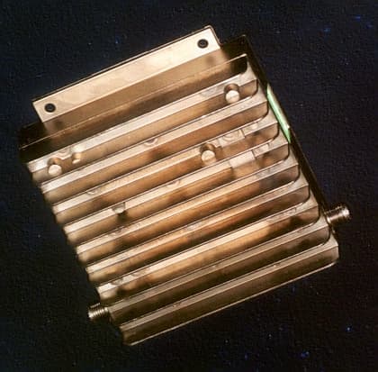
Click to zoom
Application Details
- Equipment Class
- AMP - Amplifier
- Date of Grant
- Jul 10, 2000
- Application Purpose
- Original Equipment
- Date of Application
- Mar 30, 2000
- Equipment Note
- 800 / 1900 MHz Dual Band Linear RF Compensator
- Frequency Range
- 1850.00000000 - 1910.00000000
- Company
- Motorola Mobility LLC
- Country
- United States
Documents & Files
Document Text
Text extracted from the exhibit documents filed with the FCC. Open a document above to read the original.
Users Manual
MOTOROLA, INC.FCC ID: IHDA56AJ1 Page 1 of 2 800 / 1900 MHZ DUAL BAND LINEAR RF COMPENSATOR MODEL # SYN8486A USER MANUAL 1. GENERAL The 800 / 1900 MHz Dual Band Linear RF Compensator is a bi-directional, dual band RF amplifier. It is used to compensate for signal attenuation in cellular phones due to antenna and cable losses. The device operates in both analog (AMPS) and digital (CDMA & TDMA) modes. 2. ANTENNA INSTALLATION To meet the FCC’s RF Exposure Guidelines, the antenna should be installed so there is at least 20 cm of separation between the body of the user or nearby persons and the antenna. 3. I/O CONNECTION Portable and antenna port: mini UHF type connectors. DC input and various control signals: 14-pin male connector. 4. SPECIFICATIONS Operating FrequencyTX: 824-849 MHz 1850-1910 MHz RX: 869-894 MHz 1930-1990 MHz ChannelingSingle channel Mode of TransmissionAnalog & Digital Data SourceExternal Type of ModulationAMPS (analog) CDMA (digital) TDMA (digital) Type of InformationTelephony & Data Occupied Bandwidth RequirementAMPS: 30 KHz CDMA: 1.23 MHz TDMA: 30 KHz Input PowerTX: 25 dBm max RX: 3 dBm max Output PowerTX:AMPS: 27 dBm CDMA: 27dBm TDMA: 27 dBm RX:3 dBm MOTOROLA, INC.FCC ID: IHDA56AJ1 Page 2 of 2 Harmonics & SpuriousFCC, TIA / EIA specifications StabilityAny RF load condition DC Supply Voltage 9 to 16.5 V Current Draw1.5A max RF Load VSWRFull power at better than 2:1 VSWR Operating Temp:-30 to 60°C Storage Temp-40 to 90°C
Users Manual
MOTOROLA, INC.FCC ID: IHDA56AJ1 Page 1 of 2 800 / 1900 MHZ DUAL BAND LINEAR RF COMPENSATOR MODEL # SYN8486A USER MANUAL 1. GENERAL The 800 / 1900 MHz Dual Band Linear RF Compensator is a bi-directional, dual band RF amplifier. It is used to compensate for signal attenuation in cellular phones due to antenna and cable losses. The device operates in both analog (AMPS) and digital (CDMA & TDMA) modes. 2. ANTENNA INSTALLATION To meet the FCC’s RF Exposure Guidelines, the antenna should be installed so there is at least 20 cm of separation between the body of the user or nearby persons and the antenna. 3. I/O CONNECTION Portable and antenna port: mini UHF type connectors. DC input and various control signals: 14-pin male connector. 4. SPECIFICATIONS Operating FrequencyTX: 824-849 MHz 1850-1910 MHz RX: 869-894 MHz 1930-1990 MHz ChannelingSingle channel Mode of TransmissionAnalog & Digital Data SourceExternal Type of ModulationAMPS (analog) CDMA (digital) TDMA (digital) Type of InformationTelephony & Data Occupied Bandwidth RequirementAMPS: 30 KHz CDMA: 1.23 MHz TDMA: 30 KHz Input PowerTX: 25 dBm max RX: 3 dBm max Output PowerTX:AMPS: 27 dBm CDMA: 27dBm TDMA: 27 dBm RX:3 dBm MOTOROLA, INC.FCC ID: IHDA56AJ1 Page 2 of 2 Harmonics & SpuriousFCC, TIA / EIA specifications StabilityAny RF load condition DC Supply Voltage 9 to 16.5 V Current Draw1.5A max RF Load VSWRFull power at better than 2:1 VSWR Operating Temp:-30 to 60°C Storage Temp-40 to 90°C
Users Manual
MOTOROLA, INC.FCC ID: IHDA56AJ1 Page 1 of 2 800 / 1900 MHZ DUAL BAND LINEAR RF COMPENSATOR MODEL # SYN8486A USER MANUAL 1. GENERAL The 800 / 1900 MHz Dual Band Linear RF Compensator is a bi-directional, dual band RF amplifier. It is used to compensate for signal attenuation in cellular phones due to antenna and cable losses. The device operates in both analog (AMPS) and digital (CDMA & TDMA) modes. 2. ANTENNA INSTALLATION To meet the FCC’s RF Exposure Guidelines, the antenna should be installed so there is at least 20 cm of separation between the body of the user or nearby persons and the antenna. 3. I/O CONNECTION Portable and antenna port: mini UHF type connectors. DC input and various control signals: 14-pin male connector. 4. SPECIFICATIONS Operating FrequencyTX: 824-849 MHz 1850-1910 MHz RX: 869-894 MHz 1930-1990 MHz ChannelingSingle channel Mode of TransmissionAnalog & Digital Data SourceExternal Type of ModulationAMPS (analog) CDMA (digital) TDMA (digital) Type of InformationTelephony & Data Occupied Bandwidth RequirementAMPS: 30 KHz CDMA: 1.23 MHz TDMA: 30 KHz Input PowerTX: 25 dBm max RX: 3 dBm max Output PowerTX:AMPS: 27 dBm CDMA: 27dBm TDMA: 27 dBm RX:3 dBm MOTOROLA, INC.FCC ID: IHDA56AJ1 Page 2 of 2 Harmonics & SpuriousFCC, TIA / EIA specifications StabilityAny RF load condition DC Supply Voltage 9 to 16.5 V Current Draw1.5A max RF Load VSWRFull power at better than 2:1 VSWR Operating Temp:-30 to 60°C Storage Temp-40 to 90°C
Cover Letter(s)
April 1, 2000 Federal Communications Commission Equipment Authorization Division 7435 Oakland Mills Road Columbia MD 21046 Ladies and Gentlemen, TRL Technologies, on behalf of Motorola, Inc., is applying for equipment authorization for the 800 / 1900 MHz Dual Band Linear RF Compensator, FCC ID: IHDA5Z6AJ1, model # SYN8486A. The compensator is a single channel power amplifier that will be operated under FCC Rule Part 22 and 24 and has the following specifications: Frequency Modulation Channel Power Spacing dBm W Uplink 824-849 MHz AMPS 30KHz 27 0.5 (Transmit)TDMA 30KHz 27 0.5 CDMA 1.23MHz 270.5 1850-1910 MHzAMPS 30KHz 27 0.5 TDMA 30KHz 27 0.5 CDMA 1.23MHz 270.5 Downlink 869-894 MHz AMPS 30KHz 3 0.002 (Receive)TDMA 30KHz 3 0.002 CDMA 1.23MHz 30.002 1930-1990 MHzAMPS 30KHz 3 0.002 TDMA 30KHz 3 0.002 CDMA 1.23MHz 30.002 Due to Motorola's requirement for proprietary information, we request that the following exhibits to be held confidential: 1. Block Diagrams 2. Operational Description 3. Parts List 4. Schematics Please send the grant to: Andrew Bachler FCC Liason Personal Communications Sector Motorola, Inc. 600 North U.S. Highway 45 Libertyville, IL 60048 Telephone: (847) 523-6167 Fax: (847) 523-2350 E-Mail: [email protected] If you have any questions regarding this filing, please contact me at: TRL Technologies, Inc. 2155 Stonington Ave. Suite 216 Hoffman Estates IL60195 Phone: (847) 252-5836 Fax: (847) 252-5850 Email: [email protected]
External Photos
MOTOROLA, INC.FCC ID: IHDA56AJ1 Page 1 of 1
ID Label/Location Info
MOTOROLA, INC.FCC ID: IHDA56AJ1 Page 1 of 2 MOTOROLA, INC.FCC ID: IHDA56AJ1 Page 2 of 2 SERIAL NUMBER: C AN: PENDINGF C C ID : IH D A5 Z K 1 DATE C O DE: YYDDD M O TO R O LA KIT N UM B E R : S YN8015A
Operational Description
MOTOROLA, INC.FCC ID: IHDA56AJ1 Page 1 of 2 OPERATIONAL DESCRIPTION 1. GENERAL The 800 / 1900 MHz Dual Band Linear RF Compensator is a bi-directional power amplifier. It is used to compensate for signal attenuation in cellular phones due to antenna and cable losses. It operates on a single channel, in both analog (AMPS) and digital modes (TDMA and CDMA). 2. LINEUP Cellular band: Transmit path: consists of duplexers, attenuators and RF power amplifier. Receiver path: consists of duplexers and MIMIC gain block. PCS band:Transmit path: consists of duplexers, attenuators and RF power amplifier. Receiver path: consists of duplexers, MIMIC gain blocks and attenuators. 3. I/O SIGNALS • Antenna port: PA to antenna connection. • Portable port: PA to phone connection. • ON/OFF control: control the PA’s on and off state. • RST, CLK and DATA: control signals, setting the digital potentiometer’s value. • A+: PA’s DC input power. 4. PRINCIPLES OF OPERATION Transmit signal from both cellular and PCS bands is attenuated and fed to a RF power amplifier device before going out to the antenna port. Receive signal in the cellular band is amplified and send to the portable port. Receive signal in the PCS band is amplified, attenuated and amplified again before being sent to the portable port. The PA’s gain is varied using the digital potentiometers locating in transmit paths. It is done by ways of the RST, CLK and DATA signals. The PA can be turning ON and OFF through the ON/OFF control line. MOTOROLA, INC.FCC ID: IHDA56AJ1 Page 2 of 2
Parts List/Tune Up Info
MOTOROLA, INC.FCC ID: IHDA56AJ1 800 / 1900 MHZ DUAL BAND LINEAR RF COMPENSATOR MODEL # SYN8486A ITEMQTYDESCRIPTIONREFERENCEPART # 11Diode D1 MMBD701LT1 23Diode D2 D3 D4 MMBZ5V6ALT1 31Diode, Zener D5 MMBZ5229BLT1 41Diode, Zener D6 MMBZ5242BLT1 51Diode D7 U5ZA27C 62Cellular Duplexer FIL1 FIL2 DFD0836G0881F 72Diplexer FIL3-4 SLF-080EL 82PCS Duplexer FIL5 FIL6 DFX1880J1960Q 91Transistor, FET Q1 MTD2955V 101Transistor, NPN Q2 MMBT3904LT1 113MMIC U1 U2 U11 SGA-4486 121Regulator U10 LP2951ACMX 131Regulator U12 L78L05ACD13TR 141EEPOT U3 DS1867-50 151PCS RF IC U4 RF2153 161Regulator U5 LM2941T 171Cellular RF IC U6 RF2162 182Variable Attenuator U7 U8 AV104-12 191OPAMP U9 LMC7211BIM5X Page 1 of 1
Parts List/Tune Up Info
MOTOROLA, INC.FCC ID: IHDA56AJ1 Page 1 of 1 TUNE UP PROCEDURE This tuning procedure is for reference purpose only. The PA is tuned in the factory to the specifications. There is no adjustment needed. 1. Equipment • Network analyzer • DC power supply • PC with digital potentiometer programming capability 2. Tuning Procedure • Connect the PA’s Antenna port to S11 port and Portable port to S22 port of the network analyzer. • Connect and provide all necessary signals through the 14-pin connector. • Turn on the DC supply. • Enable the PA. • Measure S21 and adjust the digital potentiometer setting for the TX port gain and power. • Measure S12 for the RX port gain and power. COMPENSATOR ON/OFF CO N TROL A+ RST CLK DATA Port 1 Port 2 NETWORK ANALYZER PS PS PC PORTABLE ANTENNA
RF Exposure Info
May 24th, 2000 SAR Test Report for Motorola’s 800 / 1900 MHz DualBand Linear RF Compensator, FCC ID IHDA56AJ1 Prepared by: Phil Aseltine, Resource Manager, Motorola Tim Avicola, Director of Engineering, TRL Technologies, Inc. Motorola and TRL Technologies, Inc. Product Safety Laboratory has reviewed the 800 / 1900 MHz DualBand Linear RF Compensator, FCC ID IHDA56AJ1, for the need to conduct SAR evaluation. Due to the design and installation of this product, it qualifies for the exclusion called out in 2.1091. The 800 / 1900 MHz DualBand Linear RF Compensator is operated as a mobile device as defined in 2.1091(b) bases on its design and installation. The compensator is installed into a vehicle such that it is physically secured and is generally located more than 20 cm from the end-user. This information is included in the user manual. It is suggested that the antenna be installed such that there is at least 20 cm of separation between the occupants of the vehicle and the antenna. The 800 / 1900 MHz DualBand Linear RF Compensator has a transmitted conducted power of 0.5 W in both cellular and PCS bands. The mobile antenna supplied with the transceiver has a maximum gain of 2.1 dBi, and minimum cable loss of –1.0 dB, together resulting in a maximum EIRP of 1 W. Since the transmit cellular band (824-849 MHz) is below 1.5 GHz and its EIRP with the supplied antenna is below 1.5 and transmit PCS band (1850-1910 MHz) is above 1.5 GHz and its EIRP with the supplied antenna is below 3W, the 800 / 1900 MHz DualBand Linear RF Compensator is categorically excluded from routine environmental evaluation per 2.1091(c).
Test Report
ENGINEERING TEST REPORT NO. 22535 ADMINISTRATIVE DATA AND SUMMARY OF TESTS DESCRIPTION OF TEST ITEM: Single Carrier Dual Band RF Linear Compensator MODEL NO: SYN8486ASERIAL NO: None Assigned MANUFACTURER: TRL Technologies APPLICABLE SPECIFICATIONS: FCC Part 22 QUANTITY OF ITEMS TESTED: One (1) TEST PERFORMED BY:ELITE ELECTRONIC ENGINEERING INCORPORATED Radio Interference Consultants Downers Grove, Illinois 60515 DATE RECEIVED: March 13, 2000 DATES TESTED: March 13 through 16, 2000 PERSONNEL (OPERATORS, OBSERVERS, AND CO-ORDINATORS): CUSTOMER: Hiep Lam of TRL Technologies was present. ELITE ELECTRONIC: Daniel E. Crowder ELITE JOB NO.: 28604 ABSTRACT: The model SYN8486A Single Carrier Dual Band RF Linear Compensator complies with the technical requirements in FCC Part 22. See test results and data pages for more details. THIS REPORT SHALL NOT BE REPRODUCED, EXCEPT IN FULL, WITHOUT THE WRITTEN APPROVAL OF ELITE ELECTRONIC ENGINEERING INCORPORATED. Page 2 of 54 ENGINEERING TEST REPORT NO. 22535 MEASUREMENT OF RF INTERFERENCE FROM A MODEL SYN8486A SINGLE CARRIER DUAL BAND RF LINEAR COMPENSATOR 1.0 INTRODUCTION: 1.1 DESCRIPTION OF TEST ITEX: During the period of March 13 through 16 , 2000, a series of radio interference measurements were performed on a model SYN8486A Single Carrier Dual Band RP Linear Compensator, (hereinafter referred to as the test item). No serial number was assigned to the test item. The tests were performed for TRL Technologies of Hoffman Estates, IL. The test item is a single carrier RF linear compensator that operates in the Cellular bands, 869MHz to 894MHz and 824MHz to 849MHz. The test item has a rated gain of l0dB. 1.2 PURPOSE: The test series was performed to determine if the test item meets the technical requirements of the FCC Part 22 for Dual Band Cellular Radio. 1.3 DEVIATIONS, ADDITIONS AND EXCLUSIONS: There were no deviations, additions to, or exclusions from the test specification during this test series. 1.4 APPLICABLE DOCUMENTS: The following documents of the exact issue designated form part of this document to the extent specified herein: - Federal Communications Commission "Code of Federal Regulations", Title 47, Part 22, dated I October 1998 - Federal Communications commission "Code of Federal Regulations", Title 47, Part 2, dated 1 October 1998 - ANSI C63.4-1992, "American National Standard for Methods of Measurement of Radio-Noise Emissions from Low-Voltage Electrical and Electronic Equipment in the Range of 9 kHz to 40 GHz" Page 4 Of 54 - TIA/EIA/IS-98-A, "Recommended Minimum Performance standards for Dual-Mode Wideband Spectrum Cellular Mobile Stations", dated July 1996 1.5 SUBCONTRACTOR IDENTIFICATION: This series of tests was performed by Elite Electronic Engineering incorporated, of Downers Grove, Illinois. The laboratory is accredited by the National Institute of Standards and Technology (NIST) under the National Voluntary Laboratory Accreditation Program (NVLAP). NVLAP Lab Code: 100278-0. 1.6 LABORATORY CONDITIONS: The temperature at the time of the test was 20°C and the relative humidity was 28%. 2.0 TEST ITEM SETUP AND OPERATION: 2.1 POWER INPUT: The test item obtained 12VDC from a Tektronix PS280 DC Power Supply through two, 1/2 meter long, unshielded leads. 2.2 GROUNDING: Since the test item was powered with 12VDC from a DC power supply, it was ungrounded during the tests. 2.3 PERIPHERAL EQUIPMENT: The following peripheral equipment was submitted with the test item: ITEM DESCRIPTION HP Signal Generator M/N E4432B, SIN VS38440973 Ophir Amplifier M/N GRF5064, SIN 1006 HP Power Meter M/N 437B, SIN 311OA05097, Next Cal 05/27/00 The output of the signal generator was routed through the amplifier. The output of the amplifier was connected to the test item through a 1 meter long coaxial cable. The power meter was connected to the test item through a 1 meter long coaxial cable. 2.4 MODULATION: The test signal was modulated with three different representative types of modulations: (1) Analog - AMPS 30kHz; (2) Digital I/Q modulations - TDMA 30kHz; CDMA 1.23 MHz. The Page 5 Of 54 ENGINEERING TEST REPORT NO. 22535 input signals were supplied from an HP M/N E4432B Signal Generator. The RF Power Output, the Occupied Bandwidth and the Spurious Emissions at Antenna Terminal tests were performed with AMPS, TDMA, and CDMA modulated input signals. The preliminary Field Strength of Spurious Emissions tests were performed with CW, AMPS, TDMA and CDMA modulated input signals. The final Field Strength of Spurious Emissions tests were performed with CW and CDMA modulated input signals. 2.5 FREQUENCY SELECTION: One test frequency was selected for each frequency band. The specified channel spacings for each modulation are shown below: Channel Modulation spacing AMPS 30kHz TDMA 30kHz CDMA 1.23MHz The specific test frequencies are designated as follows: Frequency Band (MHz) Uplink 836.5 2.6 RF POWER OUTPUT: The input levels were adjusted to reach the rated output levels shown below: Rated Rated Power Power Modulation (dBm) (Watts) AMPS 27 0.5 TDMA 27 0.5 CDMA 27 0.5 3.0 TEST EOUIPMENT: 3.1 TEST EQUIPMENT LIST: A list of the test equipment used can be found on Table 1. All equipment was calibrated per the instruction manuals supplied by the manufacturer. 3.2 CALIBRATION TRACEABILITY: Test equipment is maintained and Page 6 of 54 ENGINEERING TEST REPORT NO. 22535 calibrated on a regular basis. All calibrations are traceable to the National Institute of Standards and Technology (NIST). 4.0 REOUIREXENTS, PROCEDURES AND RESULTS: 4.1 RF POWER OUTPUT MEASUREMENTS: 4.1.1 REQUIREMENTS: In accordance with paragraph 22.913, the effective radiated power (ERP) level is allowed up to 7 watts for mobile transmitters. 4.1.2 PROCEDURES: The test item was adjusted for the rated gain. The test item was operated to measure the output for the uplink path. (a) The input signal was set to 836.5MHz. (b) The input signal was AMPS modulated. (c) The HP 437B Power Meter was connected to the outp…
Text truncated - open the document above for the full version.
Test Report
ENGINEERING TEST REPORT NO. 22536 ADMINISTRATIVE DATA AND SUMMARY OF TESTS DESCRIPTION OF TEST ITEM: Single Carrier Dual Band RF Linear Compensator MODEL NO: SYN8486A SERIAL NO: None Assigned MANUFACTURER: TRL Technologies APPLICABLE SPECIFICATIONS: FCC Part 24 QUANTITY OF ITEMS TESTED: One (1) TEST PERFORMED BY:ELITE ELECTRONIC ENGINEERING INCORPORATED Radio Interference Consultants Downers Grove, Illinois 60515 DATE RECEIVED: March 13, 2000 DATES TESTED: March 13 through 16, 2000 PERSONNEL (OPERATORS, OBSERVERS, AND CO-ORDINATORS): CUSTOMER: Hiep Lam of TRL Technologies was present. ELITE ELECTRONIC: Daniel E. Crowder ELITE JOB NO.: 28604 ABSTRACT: The model SYN8486A Single Carrier Dual Band RP Linear Compensator complies with the technical requirements in FCC Part 24. See test results and data pages for more details. THIS REPORT SHALL NOT BE REPRODUCED, EXCEPT IN FULL, WITHOUT THE WRITTEN APPROVAL OF ELITE ELECTRONIC ENGINEERING INCORPORATED. Page 2 of 141 ENGINEERING TEST REPORT NO. 22536 MEASUREMENT OF RF INTERFERENCE FROM A MODEL SYN8486A SINGLE CARRIER DUAL BAND RF LINEAR COMPENSATOR 1.0 INTRODUCTION: 1.1 DESCRIPTION OF TEST ITEM: During the period of March 13 through 16, 2000, a series of radio interference measurements were performed on a model SYN8486A Single Carrier Dual Band RF Linear Compensator, (hereinafter referred to as the test item) . No serial number was assigned to the test item. The tests were performed for TRL Technologies of Hoffman Estates, IL. The test item is a single carrier RF linear compensator that operates in the PCS bands, 1930 through 1990 and 1850 through 1910. The test item has a rated gain of 15dB. The test item is designed to operate in the following frequency ranges: Downlink Uplink Frequency Frequency Block (MHz) (MHz)_____ A 1930-1945 1850-1865 D 1945-1950 1865-1870 B 1950-1965 1870-1885 E 1965-1970 1885-1890 F 1970-1975 1890-1895 G 1975-1990 1895-1910 1.2 PURPOSE: The test series was performed to determine if the test item meets the technical requirements of the FCC Part 24 for broadband PCS. 1.3 DEVIATIONS, ADDITIONS AND EXCLUSIONS: There were no deviations, additions to, or exclusions from the test specification during this test series. Page 4 of 141 ENGINEERING TEST REPORT NO. 22536 1.4 APPLICABLE DOCUMENTS: The following documents of the exact issue designated form part of this document to the extent specified herein: - Federal Communications Commission "Code of Federal Regulations", Title 47, Part 24, dated 1 October 1998 - Federal Communications Commission "Code of Federal Regulations", Title 47, Part 2, dated 1 October 1998 - ANSI C63.4-1992, "American National Standard for Methods of Measurement of Radio-Noise Emissions from Low-Voltage Electrical and Electronic Equipment in the Range of 9 kHz to 40 GHz" 1.5 SUBCONTRACTOR IDENTIFICATION: This series of tests was performed by Elite Electronic Engineering incorporated, of Downers Grove, Illinois. The laboratory is accredited by the National Institute of Standards and Technology (NIST) under the National Voluntary Laboratory Accreditation Program (NVLAP). NVLAP Lab Code: 100278-0. 1.6 LABORATORY CONDITIONS: The temperature at the time of the test was 20"C and the relative humidity was 28%. 2.0 TEST ITEM SETUP AND OPERATION: 2.1 POWER INPUT: The test item obtained 12VDC from a Tektronix PS280 DC Power Supply through two, 1/2 meter long, unshielded leads. 2.2 GROUNDING: Since the test item was powered with 12VDC from a DC power supply, it was ungrounded during the tests. Page 5 Of 141 ENGINEERING TEST REPORT NO. 22536 2.3 PERIPHERAL EQUIPMENT: The following peripheral equipment was submitted with the test item: ITEM DESCRIPTION________________________________ HP Signal Generator M/N E4432B, S/N VS38440973 Ophir Amplifier M/N GRF5064, S/N 1006 HP Power Meter M/N 437B, SIN 3110A05097, Next Cal 05/27/00 The output of the signal generator was routed through the amplifier. The output of the amplifier was connected to the test item through a 1 meter long coaxial cable. The power meter was connected to the test item through a 1 meter long coaxial cable. 2.4 MODULATION: The test signal was modulated with three different representative types of modulations: (1) Analog - AMPS 30kHz; (2) Digital I/Q modulations - TDMA 30kHz; CDMA 1.23 MHz. The input signals were supplied from an HP M/N E4432B Signal Generator. The RF Power Output, the occupied Bandwidth and the Spurious Emissions at Antenna Terminal tests were performed with AMPS, TDMA, and CDMA modulated input signals. The preliminary Field Strength of Spurious Emissions tests were performed with CW, AMPS, TDMA and CDMA modulated input signals. The final Field Strength of Spurious Emissions tests were performed with CW and CDMA modulated input signals. Page 6 of 141 ENGINEERING TEST REPORT NO. 22536 2.5 FREQUENCY SELECTION: For test purposes, only the Uplink frequencies were tested because the test item has an antenna connection to the Uplink side only. Three test frequencies, one at the low edge, one in the middle and one at the high edge, were selected for each frequency block pair. The frequencies were one channel spacing from the low or high edge of the frequency range edge. The specified channel spacings used for each modulation type are shown below: Channel Modulation Spacing FM (AMPS) 30kHz TDMA (NADC) 30kHz CDMA 1.23MHz The specific test frequencies are designated as follows: Uplink: Low Edge Middle High Edge Modulation Frequency Frequency Frequency Block Type (MHz) (MHz) (MHz) A-D AMPS 1850.03 1860 1869.97 B-E AMPS 1870.03 1880 1889.97 F-C AMPS 1890.03 1900 1909.97 A-D NADC 1850.03 1860 1869.97 B-E NADC 1870.03 1880 1889.97 F-C NADC 1890.03 1900 1909.97 A-D CDMA 1851.23 1860 1868.77 B-E CDMA 1871.23 1880 1888.77 F-C CDMA 1890.23 1900 1908.77 2.6 RF POWER OUTPUT: The input levels were adjusted to reach the rated output levels shown below: Rated Rated Power Power Modulation (dBm) (Watts) AMPS 27 0.5 TDMA 27 0.5 CDMA 27 0.5 Page 7 of 141 ENGINEERI…
Text truncated - open the document above for the full version.
Contact Information
Applicant
Jeff Narducci(Director Product Compliance)
Technical Contact
TRL Technologies, Inc.Hiep Lam
[email protected](847) 252-5836
2155 Stonington Ave. · Hoffman Estates, Illinois · United States
Test Firm
Elite Electronic Engineering Co.Daniel Crowder
Technical Specifications
| # | Rule Parts | Frequency Range | Power Output | Emission |
|---|---|---|---|---|
| 8 | 24E | 1.85 GHz - 1.91 GHz | 500.00 mW | F9W |
Other Applications from Motorola Mobility LLC
IHDT6AC6
Sep 14, 2026Wireless Earphones
Equipment Class
JAB - Part 15 Class B Digital DeviceIHDT6AC7
Sep 11, 2026Smart Watch
Equipment Class
JAB - Part 15 Class B Digital DeviceIHDT56AX5
Aug 28, 2026Mobile Cellular Phone
Equipment Class
JBP - Part 15 Class B Computing Device PeripheralIHDT56AW9
May 12, 2026Smart Watch
Equipment Class
NII - Unlicensed National Information Infrastructure TXIHDT56AW5
Apr 08, 2026Mobile Cellular Phone
Equipment Class
DTS - Digital Transmission System