IOU0610S03Wireless LAN PC Card
National Datacomm Corporation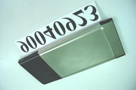
Click to zoom
Application Details
- Equipment Class
- DSS - Part 15 Spread Spectrum Transmitter
- Date of Grant
- May 20, 2001
- Application Purpose
- Original Equipment
- Date of Application
- May 20, 2001
- Equipment Note
- Wireless LAN PC Card
- Frequency Range
- 2412.00000000 - 2462.00000000
- Country
- Taiwan
Documents & Files
Document Text
Text extracted from the exhibit documents filed with the FCC. Open a document above to read the original.
Users Manual
High Speed 11Mbps Wireless LAN User’s Guide P/N: 85-506300-10 Rev. X1 March 2000 National Datacomm Corporation 4F, No. 24-2, Industry East 4th road Science Park, Hsin-Chu Taiwan, R.O.C. Technical Support E-mail: [email protected] NDC World Wide Web www.ndc.com.tw PCI/PC Card ii Instant Wave High Speed PCI/PC Card FCC WARNING This equipment has been tested and found to comply with the limits for a Class B Digital device, pursuant to part 15 of the FCC Rules. These limits are designed to provide reasonable protection against harmful interference in a residential installation. This equipment generates, uses, and can radiate radio frequency energy and, if not installed and used in accordance with the instructions, may cause harmful interference to radio communications. However, there is no guarantee that interference will not occur in a particular installation. If this equipment does cause harmful interference to radio or television reception, which can be determined by turning the equipment off and on, the user is encouraged to try to correct the interference by one or more of the following measures: ! Reorient or relocate the receiving antenna ! Increase the separation between the equipment and receiver ! Connect the equipment into an outlet on a circuit different from that to which the receiver is connected ! Consult the dealer or an experienced radio/TV technician for help You are cautioned that changes or modifications not expressly approved by the party responsible for compliance could void your authority to operate the equipment. This device complies with part 15 of the FCC Rules. Operation is subject to the following two conditions: 1. This device may not cause harmful interference, and 2. This device must accept any interference received, including interference that may cause undesired operation InstantWave High Speed PCI/PC Card iii • One Diskette for Windows NT • This User’s Guide The PC Card package should contain the following items: • One PC Card • One CD ROM (Windows Driver and Utility program) • One Diskette for Windows NT • This User’s Guide FCC Radiation Exposure Statement This equipment complies with FCC radiation exposure limits set forth for an uncontrolled environment. This equipment should be installed and operated with minimum distance 20cm between the radiator and your body. iv Instant Wave High Speed PCI/PC Card GETTING STARTED ........................................................................................... 6 H ARDWARE I NSTALLATION ................................................................................... 6 PCI Card Installation....................................................................................... 6 PC Card Installation ........................................................................................ 6 LED S .................................................................................................................... 7 D RIVER I NSTALLATION /U NINSTALLATION ............................................................ 8 Installation in Windows 95............................................................................... 8 Uninstalling the Adapter from Windows 95 ................................................... 11 Installation in Windows 98............................................................................. 12 Uninstalling the Adapter from Windows 98 ................................................... 13 Installation in Windows NT 4.0 ...................................................................... 14 Uninstalling the Adapter from Windows NT 4.0 ............................................ 15 THE INSTANTWAVE WINDOWS UTILITY PROGRAM ........................... 16 I NSTANT W AVE U TILITY I NSTALLATION .............................................................. 16 U NINSTALLING THE U TILITY P ROGRAM .............................................................. 17 SOFTWARE UPGRADE PROCEDURES ........................................................ 18 TROUBLESHOOTING....................................................................................... 19 W INDOWS 95/98 ................................................................................................. 19 Installation Problems ..................................................................................... 19 W INDOWS NT 4.0 ............................................................................................... 20 Installation Problems ..................................................................................... 20 G ENERAL ............................................................................................................ 21 Utility Error Messages ................................................................................... 21 Operational Problems .................................................................................... 21 TECHNICAL SUPPORT .................................................................................... 23 NDC LIMITED WARRANTY............................................................................ 24 InstantWave High Speed PCI/PC Card v vi Instant Wave High Speed PCI/PC Card 2 Instant Wave High Speed PCI/PC Card InstantWave Family The InstantWave PCI and PC Card are part of the InstantWave family of easy to use high performance wireless communication products. The family products include: • InstantWave High Speed PC Card (NWH610) • InstantWave High Speed PCI Card (NWH630) • InstantWave High Speed Access Point (NWH660) System Requirements Hardware Platform A station must be an x86 compatible PC with a PCI bus or PCMCIA interface. The minimum system configuration is the same as that required to run MS Windows (Windows 95, 98, NT 4.0). Software Environment The stations operate in conjunction with most of the MS Windows (Windows 95, 98, NT 4.0), Novell NetWare series. InstantWave High Speed PCI/PC Card 3 wireless network appear exactly as they would on a regular wi…
Text truncated - open the document above for the full version.
Cover Letter(s)
Federal Communications Commission Authorization and Evaluation Division Confidentiality Request Pursuant to Sections 0.457 and 0.459 of the Commission’s Rules, the Applicant hereby requests confidential treatment of information accompanying this Application as outlined below: Schematics Block Diagram Parts Lists Operational Descriptions Internal Photos The above materials contain trade secrets and proprietary information not customarily released to the public. The public disclosure of these matters might be harmful to the Applicant and provide unjustified benefits to its competitors. The Applicant understands that pursuant to Rule 0.457, disclosure of this Application and all accompanying documentation will not be made before the date of the Grant for this application. Sincerely, National Datacomm Corporation No. 2F, No. 28, Industry East 9 th Road, Science base Park, Hsinchu,Taiwan, R.O.C. Tel: +886 3 5783 966 Fax: +886 3 5630 010 FCC ID: IOU0610S03
External Photos
REPORT NO.: RF90040923Page 1Issued Date: April 23, 2001 ANNEX 2 PHOTOGRAPHS OF EUT
ID Label/Location Info
This device complies with Part 15 of the FCC rules. Operation is subject to the following two conditions: (1) This device may not cause harmful interference. (2) This device must accept any interference received, including interference that may cause undesired operation. FCC ID: IOU0610S03 P/N 83-204010-11 A1 0499
ID Label/Location Info
FCC ID LABEL LOCATION
Internal Photos
REPORT NO.: RF90040923Page 2Issued Date: April 23, 2001 REPORT NO.: RF90040923Page 3Issued Date: April 23, 2001
Test Report
FCC ID: IOU0610S03 Report No.: RF90040923 1 Issued: April 23, 2001 ANNEX 1 PROCESSING GAIN OF DIRECT SEQUENCE SPREAD SPECTRUM MEASUREMENT 1. 1.1. 1. LIMITS OF PROCESSING GAIN OF A DIRECT SEQUENCE SPREAD SPECTRUM MEASUREMENT The limit of processing gain is 10dB 1.1 TEST INSTRUMENTS & SUPPORT UNIT Description & ManufacturerModel No.Serial No. Anritsu Spectrum Analyzer, 9kHz to 30GHz MS2667CM10281 Anritsu Signal Generator, 10kHz to 20GHz 68247B984703 Hewlett Packard Power Meter,HP438A2743A04416 Hewlett Packard Power Sensor, -30 to 20dBm 8485A2942A08387 Hewlett Packard Step Attenuator, 10dB steps HP8496B3247A18505 Mini-Circuits Power SplitterZN2PD-9GNA DELL Laptop ComputerInspiron 5000eNA Campaq Laptop ComputerPPX99125 FCC ID: IOU0610S03 Report No.: RF90040923 2 Issued: April 23, 2001 1.2 METHOD OF MEASUREMENT The processing gain may be measured using the CW jamming margin method. Section 4.7.4 shows the test configuration. The test consists of stepping a signal generator in 50 kHz increments across the passband of the system. At each point, the generator level required to produce the recommended Bit Error Rate (BER) is recorded. This level is jammer level. The output power of the transmitting unit is measured at the same point. The jammer to Signal (J/S) ratio is then calculated. Discard the worst 20% of the J/S data points. The lowest remaining J/S ratio is used when calculating the Process Gain. The reference PER is specified as 8%. The corresponding Es/No (signal to noise ratio per symbol) is 16.4 dB. The curve is attached as below. This value and the measured J/S ratio are used in the following equation to calculate the Process Gain (Gp) of the system. Where: (S/N) o : Signal to noise ratio for the chosen BER. Gp = (S/N) o +Mj+Lsys FCC ID: IOU0610S03 Report No.: RF90040923 3 Issued: April 23, 2001 Mj : Maximum jammer to Signal Ratio recorded at the detected BER. Lsys : System losses . For the purpose of this processing gain calculation, we assume Lsys at its minimum value of 2 dB. TEST SETUP 7 NOTEBOOK EUT ANRITSU SIGNAL GENERATOR EUT NOTEBOOK PWR SENSOR 8485A Power meter HP 438A Mini-Circuits 15542 ZNZPD-9G HP8496D STEP ATTN 110dB (10dB steps) Matched Cables RECEIVER Transmitter FCC ID: IOU0610S03 Report No.: RF90040923 4 Issued: April 23, 2001 1.3 TEST PROCEDURES Obtain the simplex link shown. Perform all independent instrumentation calibrations prior to this procedure. Set operating power levels using fixed and variable attenuators in system to meet the following objectives: Signal Power at receiver approximately –55dBm (above thermal sensitivity such that thermal noise does not cause bit errors. Signal Power at power meter between –20 and –30dBm for optimal linearity. Use spectrum analyzer to monitor test. Ensure that CW Jammer generator RF output is disabled and measure the power at the power meter port using the power meter. This is the relative signal power, Sr. Disable Transmitter, and set CW Jammer generator RF output frequency equal to the carrier frequency and enable generator output. Set reference CW Jammer power level at power meter port 8.4dB below Sr (minimum J/S, or 10dB processing gain reference level). Note the power level setting on the generator, this is the reference CW Jammer power setting, Jr. Disable CW Jammer, re-establish link. PER test should be operating essentially error -free. Enable CW Jammer at the reference power level and verify that the PER test indicates a PER of less than 8%. Alternatively, adjust the CW Jammer level to that which causes 8% PER and verify that the S/J is less than 8.4dB. Repeat step 7 for uniform steps in frequency increments of 50 kHz across the receiver passband with the CW Jammer. In this case the receiver passband is +/- 8.5 MHz. The numerical data associated with the following radio channel is tabulated and presented for Channel 1,6, and 11. Note:Since the jamming signal will be blocked by the IF filter if the jamming frequency is far form the center of the carrier frequency. So, only those frequencies around carrier frequency are shown here. FCC ID: IOU0610S03 Report No.: RF90040923 5 Issued: April 23, 2001 1.4 EUT OPERATING CONDITION The software provided by client to set the EUT to transmit at lowest, middle and highest channel. 1.5 TEST RESULTS EUTWireless LAN PC CARDModelNWH610 NCP110 Environmental Conditions20°C, 60%RHTe s t e d B ySteven Lu Although the theoretical processing gain is lower than 10 dB, but the CCK coding provides an extra coding gain of 2.2dB. 11Mbps CHANNEL 1 Processing Gain FrequencyGp(S/N)Mj = J/SLsys (GHz)(dB)(dB)(dB)(dB) 2.4080013.016.4-4.41 2.4080512.916.4-4.51 2.4081013.516.4-3.91 2.4081513.616.4-3.81 2.4082013.216.4-4.21 2.4082513.216.4-4.21 2.4083013.016.4-4.41 2.4083512.516.4-4.91 2.4084012.416.4-5.01 2.4084512.816.4-4.61 2.4085012.916.4-4.51 2.4085512.016.4-5.41 2.4086011.916.4-5.51 2.4086511.816.4-5.61 2.4087012.016.4-5.41 2.4087512.616.4-4.81 2.4088012.116.4-5.31 2.4088512.516.4-4.91 2.4089011.816.4-5.61 2.4089511.616.4-5.81 2.4090012.016.4-5.41 2.4095011.716.4-5.71 FCC ID: IOU0610S03 Report No.: RF90040923 6 Issued: April 23, 2001 11Mbps CHANNEL 1 Processing Gain FrequencyGp(S/N)Mj = J/SLsys (GHz)(dB)(dB)(dB)(dB) 2.4095511.816.4-5.61 2.4096011.916.4-5.51 2.4096511.816.4-5.61 2.4097011.516.4-5.91 2.4097511.616.4-5.81 2.4098010.916.4-6.51 2.4098510.916.4-6.51 2.4099011.216.4-6.21 2.4099511.516.4-5.91 2.4100011.316.4-6.11 2.4100511.216.4-6.21 2.4101010.816.4-6.61 2.4101510.916.4-6.51 2.4102011.516.4-5.91 2.4102511.616.4-5.81 2.4103011.516.4-5.91 2.4103511.816.4-5.61 2.4104011.516.4-5.91 2.4104511.016.4-6.41 2.4105011.316.4-6.11 2.4105511.416.4-6.01 2.4106011.016.4-6.41 2.4106511.516.4-5.91 2.4107011.716.4-5.71 2.4107511.816.4-5.61 2.4108011.016.4-6.41 2.4108511.916.4-5.51 2.4109012.116.4-5.31 2.4109511.616.4-5.81 2.4110011.816.4-5.61 2.4110511.216.4-6.21 2.4111011.316.4-6.11 2.4111511.816.4-5.61 2.4112011.416.4-6.01 FCC ID: IOU0610S03 Report No.: RF90040923 7 Issued: April 23, 2001 11Mbps CHANNE…
Text truncated - open the document above for the full version.
Test Report
FCC ID: IOU0610S03 Report No.: RF90040923 34 Issued: April 23, 2001 4.5 POWER SPECTRAL DENSITY MEASUREMENT 4.5.1 LIMITS OF POWER SPECTRAL DENSITY MEASUREMENT The Limit of Power Spectral Density Measurement is 8dBm. 4.5.2 TEST INSTRUMENTS Description & ManufacturerModel No.Serial No.Calibrated Until ROHDE & SCHWARZ TEST RECEIVER ESMI839379/002Aug. 04, 2001 HP ATTENUATOR8496B3247A18505Cal. on use HP PLOTTER7475A2641V27755N/A Notes: 1.The measurement uncertainty is less than +/- 2.6dB, which is calculated as per the NAMAS document NIS81. 2.The calibration interval of the above test instruments is 12 months. And the calibrations are traceable to NML/ROC and NIST/USA. FCC ID: IOU0610S03 Report No.: RF90040923 35 Issued: April 23, 2001 4.5.3 TEST PROCEDURE The transmitter output was connected to the spectrum analyzer through an attenuator, the bandwidth of the fundamental frequency was measured with the spectrum analyzer using 3 kHz RBW and 30 kHz VBW, set sweep time=span/3kHz. The power spectral density was measured and recorded. The sweep time is allowed to be longer than span/3KHz for a full response of the mixer in the spectrum analyzer. 4.5.4 TEST SETUP For the actual test configuration, please refer to the related Item – Photographs of the Test Configuration. 4.5.5 EUT OPERATING CONDITION The software provided by client enabled the EUT to transmit and receive data at lowest, middle and highest channel frequencies individually. EUT SPECTRUM ANALYZER Attenuator FCC ID: IOU0610S03 Report No.: RF90040923 36 Issued: April 23, 2001 4.5.6 TEST RESULTS EUTWireless LAN PC CardModelNWH610 NCP110 Environmental Conditions 20°C, 60%RHTe s t e d B ySteven Lu CHANNEL NUMBER CHANNEL FREQUENCY (MHz ) RF POWER LEVEL IN 3 KHz BW (dBm) MAXIMUM LIMIT (dBm) PASS/FAI L 12412-10.298PASS 62437-12.528PASS 112462-13.118PASS FCC ID: IOU0610S03 Report No.: RF90040923 37 Issued: April 23, 2001 CH1 FCC ID: IOU0610S03 Report No.: RF90040923 38 Issued: April 23, 2001 CH6 FCC ID: IOU0610S03 Report No.: RF90040923 39 Issued: April 23, 2001 CH11 FCC ID: IOU0610S03 Report No.: RF90040923 40 Issued: April 23, 2001 4.6 BAND EDGES MEASUREMENT 4.6.1 LIMITS OF BAND EDGES MEASUREMENT Below –20dB of the highest emission level of operating band (in 100KHz RB). 4.6.2 TEST INSTRUMENTS Description & ManufacturerModel No.Serial No.Calibrated Until ROHDE & SCHWARZ TEST RECEIVER ESMI 848926/005 846839/018 Dec 03, 2001 HP ATTENUATOR8496B3247A18505Cal. on use HP PLOTTER7475A2641V27755N/A Notes: 1.The measurement uncertainty is less than +/- 2.6dB, which is calculated as per the NAMAS document NIS81. 2.The calibration interval of the above test instruments is 12 months. And the calibrations are traceable to NML/ROC and NIST/USA. 4.6.3 TEST PROCEDURE The transmitter output was connected to the spectrum analyzer via a low lose cable. Set both RBW and VBW of spectrum analyzer to 100 kHz with suitable frequency span including 100 kHz bandwidth from band edge. The band edges was measured and recorded. FCC ID: IOU0610S03 Report No.: RF90040923 41 Issued: April 23, 2001 4.6.4 EUT OPERATING CONDITION The software provided by client enabled the EUT to transmit and receive data at lowest, middle and highest channel frequencies individually. 4.6.5 TEST RESULTS The spectrum plots are attached below. D2 line indicates the highest level, D1 line indicates the 20dB offset below D2. It shows compliance with the requirement in part 15.247(C). FCC ID: IOU0610S03 Report No.: RF90040923 42 Issued: April 23, 2001 4.6.6 NOTE ON BAND EDGE EMISSION The band edge emission plot on page 43 shows 46.47dB delta between carrier maximum power and local maximum emission in restrict band (2.4834GHz). The emission of carrier strength list in table of page 24 is 96.1dBμV/m, so the maximum field strength in restrict band is 96.1-46.47=49.63 dBμV/m which is under 54 dBμV/m limit. FCC ID: IOU0610S03 Report No.: RF90040923 43 Issued: April 23, 2001 FCC ID: IOU0610S03 Report No.: RF90040923 44 Issued: April 23, 2001 FCC ID: IOU0610S03 Report No.: RF90040923 45 Issued: April 23, 2001 4.7 ANTENNA REQUIREMENT 4.7.1 STANDARD APPLICABLE For intentional device, according to FCC 47 CFR Section 15.203, an intentional radiator shall be designed to ensure that no antenna other than that furnished by the responsible party shall be used with the device. And according to FCC 47 CFR Section 15.247 (b), if transmitting antennas of directional gain greater than 6 dBi are used, the power shall be reduced by the amount in dB that the directional gain of the antenna exceeds 6 dBi. 4.7.2 ANTENNA CONNECTED CONSTRUCTION The antenna used in this product is Printed antenna. There is no antenna connector. And the maximum Gain of this antenna is only -1dBi. FCC ID: IOU0610S03 Report No.: RF90040923 46 Issued: April 23, 2001 5 PHOTOGRAPHS OF THE TEST CONFIGURATION CONDUCTED EMISSION TEST FCC ID: IOU0610S03 Report No.: RF90040923 47 Issued: April 23, 2001 RADIATED EMISSION TEST FCC ID: IOU0610S03 Report No.: RF90040923 48 Issued: April 23, 2001 6 INFORMATION ON THE TESTING LABORATORIES We, ADT Corp., were founded in 1988 to provide our best service in EMC and Safety consultation. Our laboratories are accredited by the following approval agencies according to ISO/IEC Guide 25 or EN 45001: USA FCC, NVLAP Germany TUV Rheinland Japan VCCI New Zealand RFS Norway NEMKO, DNV U.K. INCHCAPE R.O.C. BSMI Copies of accreditation certificates of our laboratories obtained from approval agencies can be downloaded from our web site: www.adt.com.tw/index.5/phtml. If you have any comments, please feel free to contact us at the following: Lin Kou EMC Lab: Tel: 886-2-26052180 Fax: 886-2-26052943 Hsin Chu EMC Lab: Tel: 886-35-935343 Fax: 886-35-935342 Lin Kou Safety Lab: Tel: 886-2-26093195 Fax: 886-2-26093184 Design Center: Tel: 886-2-26093195 Fax: 886-2-26093184 Email: [email protected] Web Site: www.adt.com.tw
Test Report
FCC ID: IOU0610S03 Report No.: RF90040923 1 Issued: April 23, 2001 FCC TEST REPORT REPORT NO.: RF90040923 MODEL NO.: NWH610 NCP110 RECEIVED: April 9, 2001 TESTED: April 20, 2001 APPLICANT: NATIONAL DATACOMM CORPORATION ADDRESS: 4F, No.24-2, Industry East 4 th Road, Science Park, Hsinchu, Taiwan, R.O.C. ISSUED BY: Advance Data Technology Corporation LAB LOCATION: 47, 14 th Lin, Chiapao Tsuen, Linkou, Taipei 244, Taiwan, R.O.C. This test report consists of 48 pages in total. It may be duplicated completely for legal use with the approval of the applicant. It should not be reproduced except in full, without the written approval of our laboratory. The client should not use it to claim product endorsement by NVLAP or any U.S. government agencies. The test results in the report only apply to the tested sample. Accredited Laboratory FCC ID: IOU0610S03 Report No.: RF90040923 2 Issued: April 23, 2001 Table of Contents 1CERTIFICATION .................................................................................................. 4 2SUMMARY OF TEST RESULTS......................................................................... 5 3GENERAL INFORMATION ................................................................................ 6 3.1GENERAL DESCRIPTION OF EUT .................................................................................. 6 3.2DESCRIPTION OF TEST MODES ..................................................................................... 6 3.3GENERAL DESCRIPTION OF APPLIED STANDARDS ................................................. 7 3.4DESCRIPTION OF SUPPORT UNITS ............................................................................... 7 4TEST PROCEDURES AND RESULTS ............................................................... 8 4.1CONDUCTED EMISSION MEASUREMENT................................................................... 8 4.1.1LIMITS OF CONDUCTED EMISSION MEASUREMENT .............................................................8 4.1.2TEST INSTRUMENTS ......................................................................................................................8 4.1.3TEST PROCEDURES ........................................................................................................................9 4.1.4TEST SETUP ....................................................................................................................................10 4.1.5TEST RESULTS ...............................................................................................................................11 4.2RADIATED EMISSION MEASUREMENT ..................................................................... 17 4.2.1LIMITS OF RADIATED EMISSION MEASUREMENT................................................................17 4.2.2TEST INSTRUMENTS ....................................................................................................................18 4.2.3TEST PROCEDURES ......................................................................................................................19 4.2.4TEST SETUP ....................................................................................................................................20 4.2.5TEST RESULTS ...............................................................................................................................21 4.36dB BANDWIDTH MEASUREMENT ............................................................................. 25 4.3.1LIMITS OF 6dB BANDWIDTH MEASUREMENT .......................................................................25 4.3.2TEST INSTRUMENTS ....................................................................................................................25 4.3.3TEST PROCEDURE.........................................................................................................................26 4.3.4TEST SETUP ....................................................................................................................................26 4.3.5EUT OPERATING CONDITION.....................................................................................................26 4.3.6TEST RESULTS ...............................................................................................................................27 4.4MAXIMUM PEAK OUTPUT POWER............................................................................. 31 4.4.1LIMITS OF MAXIMUM PEAK OUTPUT POWER MEASUREMENT........................................31 4.4.2INSTRUMENTS...............................................................................................................................31 4.4.3TEST PROCEDURES ......................................................................................................................32 4.4.4TEST SETUP ....................................................................................................................................32 4.4.5EUT OPERATING CONDITION.....................................................................................................32 4.4.6TEST RESULTS ...............................................................................................................................33 4.5POWER SPECTRAL DENSITY MEASUREMENT ........................................................ 34 4.5.1LIMITS OF POWER SPECTRAL DENSITY MEASUREMENT ..................................................34 4.5.2TEST INSTRUMENTS ....................................................................................................................34 FCC ID: IOU0610S03 Report No.: RF90040923 3 Issued: April 23, 2001 4.5.3TEST PROCEDURE.........................................................................................................................35 4.5.4TEST SETUP ....................................................................................................................................35 4.5.5EUT OPERATING CONDITION...............................…
Text truncated - open the document above for the full version.
Test Setup Photos
FCC ID: IOU0610S03 Report No.: RF90040923 46 Issued: April 23, 2001 5 PHOTOGRAPHS OF THE TEST CONFIGURATION CONDUCTED EMISSION TEST FCC ID: IOU0610S03 Report No.: RF90040923 47 Issued: April 23, 2001 RADIATED EMISSION TEST
Contact Information
Applicant
Jerome Wu(Director)
886 3 578-3966Fax: 886 3 577-7989
Test Firm
Bureau Veritas CPS (H.K.) Ltd. Taoyuan BranchRichard Chen
Technical Specifications
| # | Rule Parts | Frequency Range | Power Output |
|---|---|---|---|
| 1 | 15C | 2.41 GHz - 2.46 GHz | 77.00 mW |
Other Applications from National Datacomm Corporation
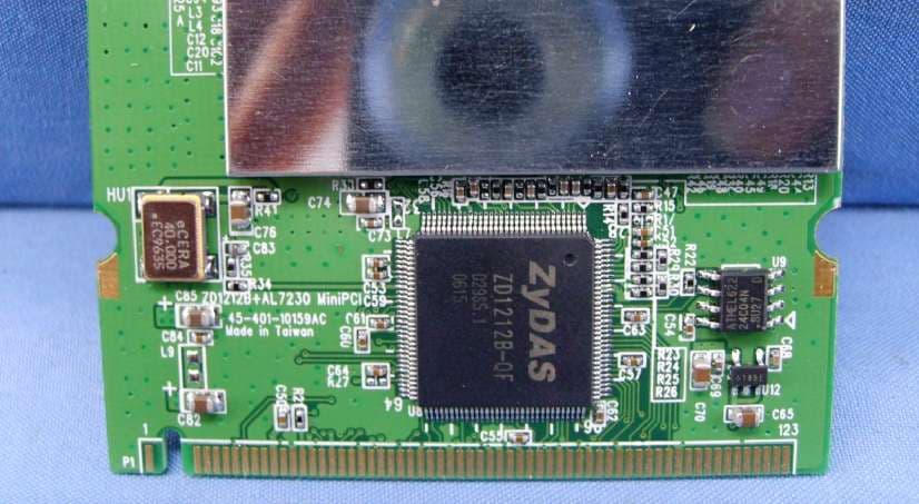
IOU-NWH3054A
Sep 24, 2006IEEE802.11a/g/b NWH3054A WLAN mini-PCI
Equipment Class
DTS - Digital Transmission System
IOU3050S01
Feb 26, 2004802.11g+ MiniPCI Module
Equipment Class
DTS - Digital Transmission System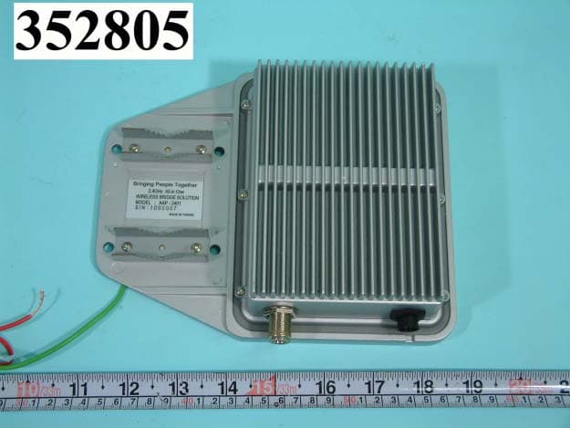
IOU9210S01
Sep 10, 2003OUTDOOR BRIDGE
Equipment Class
DTS - Digital Transmission System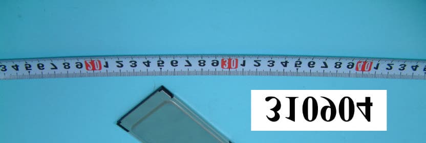
IOU1021S01
Feb 26, 2003WLAN PCMCIA Adapter
Equipment Class
DTS - Digital Transmission System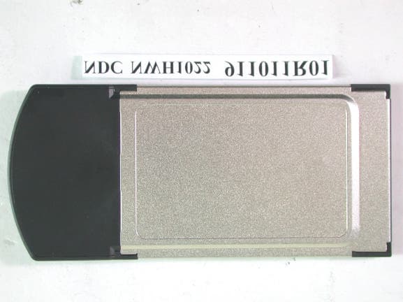
IOU1022S01
Oct 30, 200222Mbps Cardbus Adapter
Equipment Class
DTS - Digital Transmission System