IZ3-TT-7000-TAuxiliary Broadcast Transmitter
TRON Tek Inc
Click to zoom
Application Details
- Equipment Class
- TBC - Licensed Broadcast Station Transmitter
- Date of Grant
- Nov 11, 2002
- Application Purpose
- Original Equipment
- Date of Application
- Sep 08, 2002
- Equipment Note
- Auxiliary Broadcast Transmitter
- Frequency Range
- 6875.00000000 - 7126.00000000
- Company
- TRON Tek Inc
- Country
- United States
Documents & Files
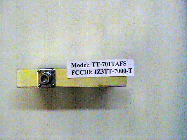
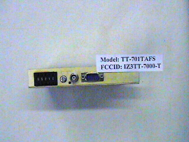
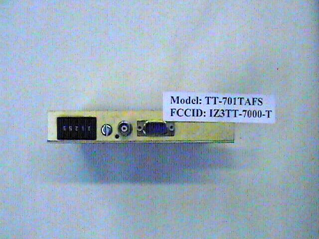
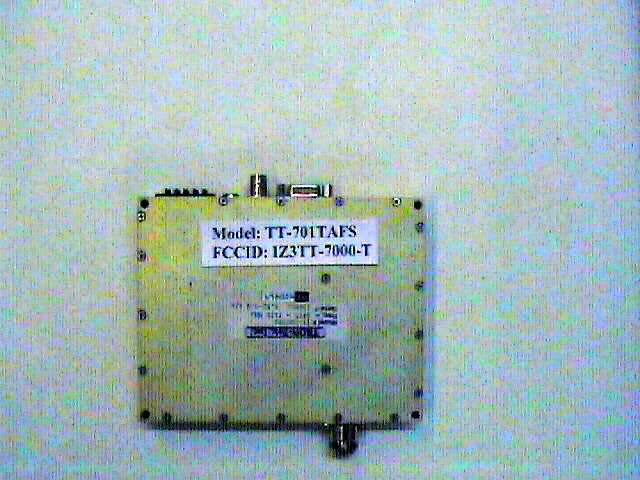
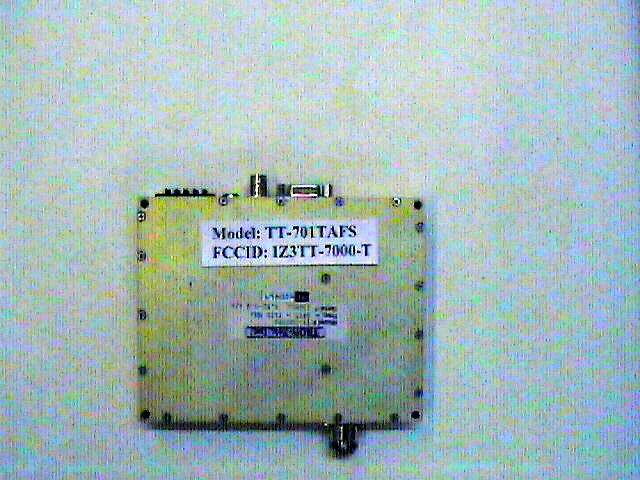
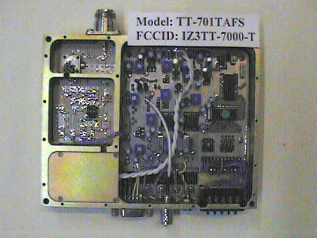
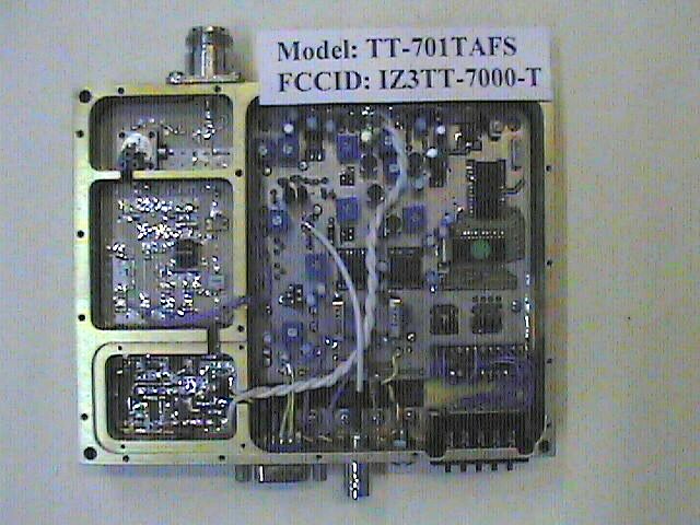
Document Text
Text extracted from the exhibit documents filed with the FCC. Open a document above to read the original.
Users Manual
Owner-Service Manual TT-7 000TS-AB The Tron-Tek transmitter does not require an Owner-Service Manual. The transmitter installs into various other end unit components. The end units, such as Tower Cameras and Repeater Systems, contain owner- service manuals for explanation of the units. The transmitter is simply a component in a larger system.
Block Diagram
Theory Of Operation: Block Diagram
ID Label/Location Info
FCC LABELING REQUIREMENTS TRON-Tek, Inc. FCC ID : I Z 3-TT-7000-T This device complies with part 15 of the FCC Rules. Operationis subject to the following two conditions: (1) This device may not cause harmful interference, and (2) this device must accept any interference that may cause undesired operation. FCC Part 15 Compliance Statement FCC Identifying Label
Operational Description
Circuit Board Prints TT-7 000TS-AB
Operational Description
Theory of Operation TT-7 000TS-AB THEORY OF OPERATION: Control Board Assembly Power Supplies: Power is supplied through J1. Pins 1 and 2 are +12 volts; pins 3 and 4 are ground. Ferrite beads are used on all connections on J1 to minimize RF leakage to the power lines. C1 and C2 provide additional RF filtering of the 12 volts before it passes through D1, which provides reverse polarity protection for the transmitter. Filter capacitors are used on the inputs and outputs of the regulators to prevent unwanted oscillations. U2 is a fixed +5 volt regulator used primarily for the logic and prescaler circuits. U1 is a fixed +8 volt regulator used for the audio, video circuits and miscellaneous operational amplifiers. Q2, 5, 6, and R8-15 form a variable voltage regulator for the driver FET that is adjusted by R14 for proper drive levels to the final amplifier. Q1, 3, 4 and R2-6 form a variable voltage regulator for the final amplifier. R16- 20 and S1 are placed in the feedback portion of the regulator to provide a selectable voltage output to the PA. Selection of the voltage applied to the final amplifier allows different power levels to be achieved. R19 sets power output to 12 Watt while R20 sets the output power to 2 Watts. R37-40, 51, C36-40, C95, and U5 Generates the negative 2-volt bias required for the FET’s on the PA. Q7 and Q8 disable the variable voltage regulators to prevent power from being applied to the PA until the PLL provides a lock detect condition. R44 and C27 remove the narrow pulses originating from the lock detect output of U6 pin 28. Video circuits: Video is connected through J2 to the 525-line video pre-emphasis network of R22-26, C12, and L1. R25 allows for the adjustment of the network due to tolerance deviation of components. This network also forms a 75-ohm termination for the video. D4 and D5 provide deviation limiting. R28 adjusts video deviation of the transmitter. C11 and C13 remove the D.C. component of the video signal. Audio circuits: Audio for sub-carrier 1 is connected through pins 6 (high) and 7 (low) of J1 to T1, which is configured as a 600-ohm balanced coupling transformer. The output of T1 is terminated with R79 and A.C. coupled to U7 by C48. U7 is a dual gain control circuit. Channel 1(pins 1,2,3,5,6,7,8) is configured to amplify the audio while channel 2 (pins 9,10,11,12,14,15,16) acts as a limiter and provides a 2: 1 compression of the audio signal. R62-64, C59-61 and Q11 form a three pole 10 KHz low-pass filter. R65 is used to adjust the deviation of the sub-carrier. R66-70, C62-65, L2, D8, and Q12 form a series tuned colpitts oscillator. L2 is a variable inductor for tuning the frequency of the oscillator. Sub-carrier frequencies available are 4.83Mhz, 5.8Mhz, 6.2Mhz, 6.8Mhz and 7.5Mhz. C62 couples the audio to the oscillator. D8 is the varactor diode, which modulates the sub carrier. Q13 is a buffer amplifier and L3 and C67 provides tuning (peaking) for the amplifier. R74 is used to adjust the sub- carrier insertion level. THEORY OF OPERATION: Control Board Assembly Audio circuits: Audio for sub-carrier 2 is connected through pins 8 (high) and 9 (low) of J1 to T2, which is configured as a 600-ohm balanced coupling transformer. The output of T2 is terminated with R78 and A.C. coupled to U8 by C71. U8 is a dual gain control circuit. Channel 1(pins 1,2,3,5,6,7,8) is configured to amplify the audio while channel 2 (pins 9,10,11,12,14,15,16) acts as a limiter and provides a 2: 1 compression of the audio signal. R86-88, C82-84 and Q14 form a three pole 10 KHz low-pass filter. R89 is used to adjust the deviation of the sub-carrier. R90-94, C85-88, L4, D9, and Q15 form a series tuned colpitts oscillator. L2 is a variable inductor for tuning the frequency of the oscillator. Sub-carrier frequencies available are 4.83Mhz, 5.8Mhz, 6.2Mhz, 6.8Mhz and 7.5Mhz. C85 couples the audio to the oscillator. D9 is the varactor diode, which modulates the sub carrier. Q16 is a buffer amplifier and L5 and C90 provides tuning (peaking) for the amplifier. R98 is used to adjust the sub- carrier insertion level. PLL circuits: PLL IC: It is beyond the scope of this document to discuss the theory of Phase Locked Loop design only the support circuits and operation will be detailed. U6 is a low frequency CMOS PLL. It contains a reference oscillator, selectable-reference divider, two output phase detector, 10-bit programmable divide-by-N counter, 6-bit programmable divide-by-A counter, dual modulus controller, and a lock detect circuit. If combined with a VCO, dual modulus, and loop filter, then frequency synthesis up to the devices frequency limit can be achieved. Tron-Tek, Inc. equipment also incorporates a Micro-Controller to allow operation only within the user designated frequencies of 1990- 2110, 2025-2135 and 2450-2499. Additionally this equipment utilizes an external temperature compensated reference oscillator (TCXO). VCO: See VCO section for description. Dual Modulus: U4 is a Dual Modulus which divides the VCO frequency by 64 or 65 depending on the status of the A counter within U6. Control of the divide ratio is provided by U6 pin 9. R36 provides proper input load. C28 A.C. couples the VCO frequency into U4. R53 provides an output load while C34 A.C. couples the output of U4 into the U6 Pin 1. The A and N counter then divide this frequency and present it to the phase detector for comparison to the reference frequency. C31-33 and C35 provide de-coupling for U4. THEORY OF OPERATION: Control Board Assembly PLL circuits: Loop Filter/Buffer: R45-50, C17-25, and U3 form the low pass loop filter. This filter removes the narrow pulses inherent in the phase detector and provides a loop error signal. The video, audio and loop filter signals are summed at the base of Q9, which buffers this signal. R35 provides a load for the buffer and R34 decouples the high frequency of the VCO while coupling the control voltage to the VCO. TCXO: R41, R43, R52, R100, C42, C43, Q10, Y1, and C45-47 form…
Text truncated - open the document above for the full version.
Parts List/Tune Up Info
Control Board Active Part List NumberQuantityPart NumberPart DesignatorDescriptionManufacturer 12MMBT2222Q5, Q6SOT-23 TransistorAny 22PN2222Q3, Q4TO-92 TransistorAny 38MMBTH10Q9, Q10, Q11, Q12SOT-23 TransistorAny Q13, Q14,Q15, Q16 42MMBF4393LT1Q7, Q8SOT-23 TransistorMotorola 52836AD8, D9SOT-23 DiodeAny 6178LO8U1TO-220 8V RegAny 7178LO5U2TO-220 5V RegAny 8112022ADU3SO-8 Dual ModMotorola 91LM358U4SO-8 Op AmpHarris 101Max 851U5SO-8 Neg BiasMaxim 111MC145152DW2U6SOG-28 PLLMotorola 122NE570U7, U8SO-16 CompndrPhillips 131MC68HC705E5DWU9SOG-28 ProcMotorola 14116 Mhz CrystalY1CrystalAny 15132 Mhz CrystalY2CrystalAny 162IRF 9520Q1, Q2TO-220 FetIRF 171MBR1045D1TO-220 DiodeMotorola
Parts List/Tune Up Info
Tune-Up Procedures TT-7 000TS-AB The Tron-Tek transmitter does not requires user-end tune-up procedures. This unit installs into various other units, including Tower Cameras and Repeater Systems. The tune-up procedures are provided for the finished product.
Schematics
VCO_Schematic_FCC VCO_Schematic_FCC Jerel Byrd CustomMay 07, 2002 00011.0 11 Title: Designed by: Checked by: Approved by: SizeDate Document NRevision Sheetof 0 0 1 1 2 2 3 3 4 4 5 5 6 6 7 7 8 8 9 9 10 10 11 11 12 12 13 13 14 14 15 15 16 16 17 17 18 18 19 19 20 20 21 21 22 22 23 23 24 24 25 25 AA BB CC DD EE FF GG HH II JJ KK LL MM NN OO PP QQ RR R8C1 R9C21 Control_Volts_In D1 Q1 R13R12 C24 L2 C3 R2 R11 R1C2 C4C5C6C7 C25 R10 R20 Q2 R14 C17 L3 R4R5 C18 C28 R3 C8C9C10C11C12 10_Volts L7 C20 L4 R6R7 C19 L8 Q3 C59C58C57C56C55 L9L10 R18 Q4 L5 L1R19R17R15 L6 VCO_Output C44 C23 VCC Gnd Gnd1 Bypass U1 Input Output 5_Volts C34C35 C33 C36 Frequency_to_PLL Supply Voltage RF Signal RF Signal Supply Voltage 12 Ohm 22 Ohm 470 Ohm 2.2 K 10 K 220 Ohm R17 R19 R12 R13 R3 R20 R4 R5 R6 R7 R9 R11 R1 R2 R18 R14 MA46H201 VARACTOR MRF9411 NPN TRANS. UPB1508GV DIVIDE BY 2 NE325501 GAASFET Q1 Q2 Q3 Q4 D1 U1 0.2 pF CAPACITOR 1.0 pF CAPACITOR 3.3pF CAPACITOR 1.5 pF CAPACITOR C22 C23 C28 C37 C55 C56 C57 C58 C59 C60 C24 C25 C32 C38 C42 C45 27 pF CAPACITOR 220 pF CAPACITOR 0.1uF CAPACITOR 1nF CAPACITOR C4 C10 C15 C27 C30 C36 C40 C43 C47 C52 C5 C9 C14 C26 C29 C33 C35 C41 C44 C48 C1 C2 C3 C7 C8 C11 C13 C16 C17 C18 C19 C20 C21 C31 C39 C46 C50 C6 C12 C34 0.33uF CAPACITOR C49 C51 C53 C54 51 OhmR8 R15 75 OhmR10 C60 C22 C37 C32 C42 C13C14C15C16 C26 C27 C29C30C31 C38C39C40C41C43C45C46 C47C48C49C50C51C52C53C54
Test Report
FCC ID: IZ3-TT-7000-T MFA p0280004, d0290012 Date: September 9, 2002 Federal Communications Commission Via: Electronic Filing Attention: Authorization & Evaluation Division Applicant: Tron-Tek, Inc. Equipment: TT-701TAFS FCC ID: IZ3-TT-7000-T FCC Rules: 74.601 Gentlemen: On behalf of the Applicant, enclosed please find Application Form 731, Engineering Test Report and all pertinent documentation, the whole for approval of the referenced equipment as shown. Filing fees are attached. We trust the same is in order. Should you need any further information, kindly contact the writer who is authorized to act as agent. Sincerely yours, Morton Flom, P. Eng. enclosure(s) cc: Applicant MF/cva FCC ID: IZ3-TT-7000-T MFA p0280004, d0290012 LIST OF EXHIBITS (FCCCERTIFICATION(TRANSMITTERS) - REVISED 9/28/98) APPLICANT: Tron-Tek, Inc. FCC ID: IZ3-TT-7000-T BY APPLICANT: 1. LETTER OF AUTHORIZATION x 2. IDENTIFICATION DRAWINGS, 2.1033(c)(11) xLABEL xLOCATION OF LABEL xCOMPLIANCE STATEMENT xLOCATION OF COMPLIANCE STATEMENT 3. PHOTOGRAPHS, 2.1033(c)(12) x 4. DOCUMENTATION: 2.1033(c) (3) USER MANUAL x (9) TUNE UP INFO x (10) SCHEMATIC DIAGRAM x (10) CIRCUIT DESCRIPTION x BLOCK DIAGRAM x PARTS LIST x ACTIVE DEVICES x 5. MPE REPORT x BY M.F.A. INC. A. TESTIMONIAL & STATEMENT OF CERTIFICATION B. STATEMENT OF QUALIFICATIONS FCC ID: IZ3-TT-7000-T MFA p0280004, d0290012 TRANSMITTER CERTIFICATION of FCC ID: IZ3-TT-7000-T MODEL: TT-701TAFS to FEDERAL COMMUNICATIONS COMMISSION Rule Part(s) 74.601 DATE OF REPORT: September 9, 2002 ON THE BEHALF OF THE APPLICANT: Tron-Tek, Inc. AT THE REQUEST OF : P.O. LJ081302 Tron-Tek, Inc. 6570-B E. 51st St. Tulsa, OK 74145 Attention of: Mr. W. M. Grass, President (918) 663-4877; FAX: 664-0309 [email protected] SUPERVISED BY: Morton Flom, P. Eng. FCC ID: IZ3-TT-7000-T MFA p0280004, d0290012 THE APPLICANT HAS BEEN CAUTIONED AS TO THE FOLLOWING: 15.21 INFORMATION TO USER. The users manual or instruction manual for an intentional radiator shall caution the user that changes or modifications not expressly approved by the party responsible for compliance could void the user's authority to operate the equipment. 15.27(a) SPECIAL ACCESSORIES. Equipment marketed to a consumer must be capable of complying with the necessary regulations in the configuration in which the equipment is marketed. Where special accessories, such as shielded cables and/or special connectors are required to enable an unintentional or intentional radiator to comply with the emission limits in this part, the equipment must be marketed with, i.e. shipped and sold with, those special accessories. However, in lieu of shipping or packaging the special accessories with the unintentional or intentional radiator, the responsible party may employ other methods of ensuring that the special accessories are provided to the consumer, without additional charge. Information detailing any alternative method used to supply the special accessories for a grant of equipment authorization or retained in the verification records, as appropriate. The party responsible for the equipment, as detailed in § 2.909 of this chapter, shall ensure that these special accessories are provided with the equipment. The instruction manual for such devices shall include appropriate instructions on the first page of text concerned with the installation of the device that these special accessories must be used with the device. It is the responsibility of the user to use the needed special accessories supplied with the equipment. FCC ID: IZ3-TT-7000-T MFA p0280004, d0290012 TABLE OF CONTENTS RULEDESCRIPTIONPAGE . Test Report 1 2.1033(c) General Information Required 2 2.1033(c)(14) Rule Summary 5 . Standard Test Conditions and Engineering Practices 6 2.1046(a) Carrier Output Power (Conducted) 7 2.1046(a) ERP Carrier Power (Radiated) 9 2.1051 Unwanted Emissions (Transmitter Conducted) 10 2.1053(a) Field Strength of Spurious Radiation 13 2.1049(c)(1) Emission Masks (Occupied Bandwidth) 17 2.1047(a) Audio Low Pass Filter (Voice Input) 23 2.1055(a)(1) Frequency Stability (Temperature Variation) 26 2.1055(b)(1) Frequency Stability (Voltage Variation) 29 2.202(g) Necessary Bandwidth and Emission Bandwidth 30 FCC ID: IZ3-TT-7000-T MFA p0280004, d0290012 PAGE NO.1of30. Required information per ISO/IEC Guide 25-1990, paragraph 13.2: a) TEST REPORT b) Laboratory: (FCC: 31040/SIT) (Canada: IC 2044) M. Flom Associates, Inc. 3356 N. San Marcos Place, Suite 107 Chandler, AZ 85225 c) Report Number: d0290012 d) Client: Tron-Tek, Inc. 6570-B E. 51st St. Tulsa, OK 74145 e) Identification: TT-701TAFS FCC ID: IZ3-TT-7000-T EUT Description: Auxiliary Broadcast Transmitter f) EUT Condition: Not required unless specified in individual tests. g) Report Date: September 9, 2002 EUT Received: 2002-Aug-19 h, j, k): As indicated in individual tests. i) Sampling method: No sampling procedure used. l) Uncertainty: In accordance with MFA internal quality manual. m) Supervised by: Morton Flom, P. Eng. n) Results: The results presented in this report relate only to the item tested. o) Reproduction: This report must not be reproduced, except in full, without written permission from this laboratory. FCC ID: IZ3-TT-7000-T MFA p0280004, d0290012 PAGE NO.2of30. LIST OF GENERAL INFORMATION REQUIRED FOR CERTIFICATION IN ACCORDANCE WITH FCC RULES AND REGULATIONS, VOLUME II, PART 2 AND TO 74.601 Sub-part 2.1033 (c)(1): NAME AND ADDRESS OF APPLICANT: Tron-Tek, Inc. 6570-B E. 51st St. Tulsa, OK 74145 MANUFACTURER: Tron-Tek, Inc. (c)(2): FCC ID: IZ3-TT-7000-T MODEL NO: TT-701TAFS (c)(3): INSTRUCTION MANUAL(S): PLEASE SEE ATTACHED EXHIBITS (c)(4): TYPE OF EMISSION: 18N0F5W, 18N0F9W (c)(5): FREQUENCY RANGE, MHz : 6875 to 7126 (c)(6): POWER RATING, Watts: 1.0 Switchable Variable x N/A FCC GRANT NOTE: M4 - Operation of this unit is limited to use at stations licensed for use under Part 74 of FCC Rules. (c)(7): MAXIMUM POWER RATING, Watts: DUT RESULTS : Passes x Fails FCC ID: IZ3-TT-7000-T MFA p0280004, d0290…
Text truncated - open the document above for the full version.
Test Report
FCC ID: IZ3-TT-7000-T MFA p0280004, d0290012 PAGE NO.2 of 30. AMENDED November 6, 2002 LIST OF GENERAL INFORMATION REQUIRED FOR CERTIFICATION IN ACCORDANCE WITH FCC RULES AND REGULATIONS, VOLUME II, PART 2 AND TO 74.601 Sub-part 2.1033 (c)(1): NAME AND ADDRESS OF APPLICANT: Tron-Tek, Inc. 6570-B E. 51st St. Tulsa, OK 74145 MANUFACTURER: Tron-Tek, Inc. (c)(2): FCC ID: IZ3-TT-7000-T MODEL NO: TT-701TAFS (c)(3): INSTRUCTION MANUAL(S): PLEASE SEE ATTACHED EXHIBITS (c)(4): TYPE OF EMISSION: 6M25C3F (c)(5): FREQUENCY RANGE, MHz : 6875 to 7126 (c)(6): POWER RATING, Watts: 1.0 Switchable Variable x N/A FCC GRANT NOTE: M4 - Operation of this unit is limited to use at stations licensed for use under Part 74 of FCC Rules. DUT RESULTS: Passes x Fails FCC ID: IZ3-TT-7000-T MFA p0280004, d0290012 PAGE NO.19 of 30. AMENDED November 6, 2002 NAME OF TEST: Emission Masks (Occupied Bandwidth) g0280146: 2002-Aug-20 Tue 09:49:00 STATE: 2:High Power CORR'D RES BW 30 kHz VBW 30 kHz SWP 90.0 msec ATTEN 10 dBREF 30.0 dBm 10 dB/ POS PK CENTER 7.000 6 GHz SPAN 30.0 MHz OFFSET 39.0 dB MKR 7.001 07 GHz 25.40 dBm POWER: HIGH MODULATION: 5.75 MHz @ 1 Volt PERFORMED BY: Doug Noble, B.A.S. E.E.T. FCC ID: IZ3-TT-7000-T MFA p0280004, d0290012 PAGE NO.20 of 30. AMENDED November 6, 2002 NAME OF TEST: Emission Masks (Occupied Bandwidth) g0280147: 2002-Aug-20 Tue 09:50:00 STATE: 2:High Power CORR'D RES BW 30 kHz VBW 30 kHz SWP 300 msec ATTEN 10 dBREF 30.0 dBm 10 dB/ POS PK CENTER 7.000 GHz SPAN 100 MHz OFFSET 39.0 dB MKR 7.001 3 GHz 25.40 dBm POWER: HIGH MODULATION: 5.75 MHz @ 1 VOLT PART 74.602 PERFORMED BY: Doug Noble, B.A.S. E.E.T.
Contact Information
Applicant
W M Grass(President)
Technical Contact
M. Flom Associates, IncMorton Flom
[email protected]480 926 3100
3356 N. San Marcos Pl., Suite 107 · Chandler, Arizona · United States
Non-Technical Contact
M. Flom Associates, Inc.Morton Flom
[email protected]480 926 3100
Test Firm
M. Flom Associates, Inc.Morton Flom
Technical Specifications
| # | Rule Parts | Frequency Range | Power Output | Emission | Tolerance |
|---|---|---|---|---|---|
| 1 | 74 | 6.88 GHz - 7.13 GHz | 1 W | 18M0F9W | 0.0020000000 % |
Other Applications from TRON Tek Inc

IZ3-TT-2012TS-AB
Dec 14, 2000Auxiliary Broadcast Transmitter
Equipment Class
TBC - Licensed Broadcast Station TransmitterIZ3-TT-450-T
Aug 23, 1994TNB - Licensed Non-Broadcast Station Transmitter
Equipment Class
TNB - Licensed Non-Broadcast Station TransmitterIZ3TT-450-R
Aug 14, 1994UHF Data Receiver
Equipment Class
CXX - Communications Rcvr for use w/ licensed Tx and CBsIZ3-TT-2000-T
Oct 11, 1993TBC - Licensed Broadcast Station Transmitter
Equipment Class
TBC - Licensed Broadcast Station TransmitterIZ3-TT-2400-T
Jan 12, 1993TNB - Licensed Non-Broadcast Station Transmitter
Equipment Class
TNB - Licensed Non-Broadcast Station Transmitter