JCK-GN-WLM01WLAN PCMCIA Card
GIGA-BYTE TECHNOLOGY CO., LTD.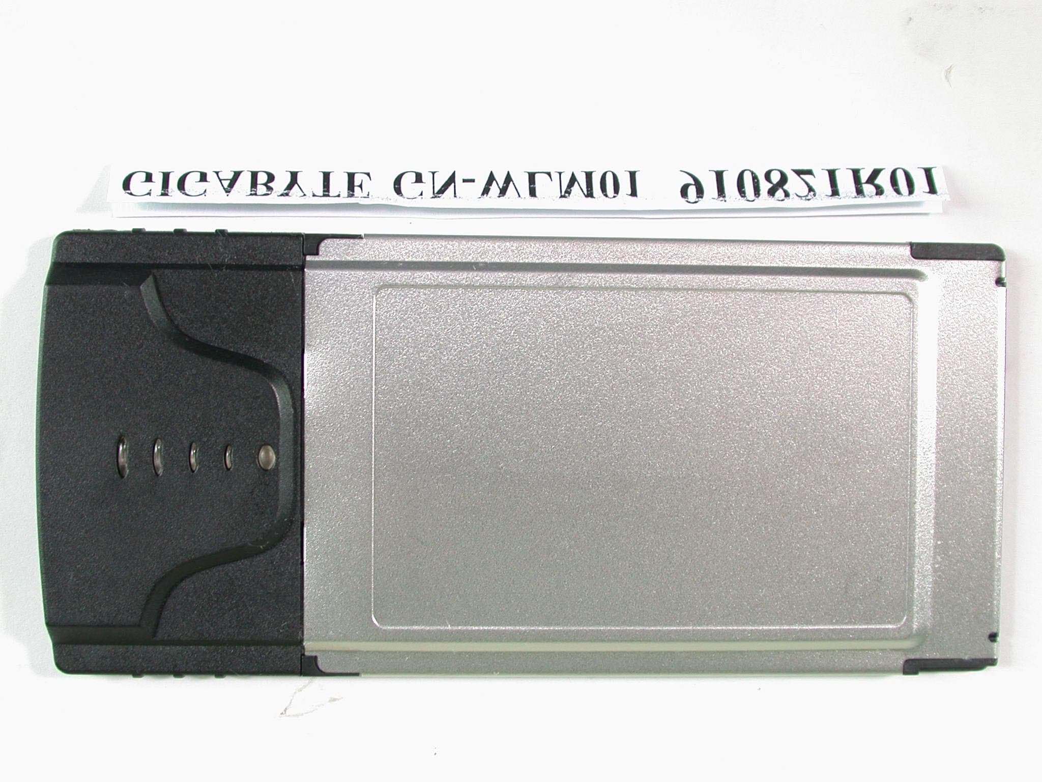
Click to zoom
Application Details
- Equipment Class
- DSS - Part 15 Spread Spectrum Transmitter
- Date of Grant
- Sep 24, 2002
- Application Purpose
- Original Equipment
- Date of Application
- Sep 24, 2002
- Equipment Note
- WLAN PCMCIA Card
- Frequency Range
- 2412.00000000 - 2462.00000000
- Country
- Taiwan
Documents & Files
Document Text
Text extracted from the exhibit documents filed with the FCC. Open a document above to read the original.
Users Manual
1 GN-WLM01 IEEE 802.11b PCMCIA Wireless Adapter User’s Manual 2 Contents Chapter1. Product Overview 1-1. Introduction to The Client Adapter ........................3 1-2. Features ........................3 1-3. Physical Dimension/Packaging ........................3 1-4. LED Display Indicator ........................4 1-5. System Requirements ........................4 Chapter2. Installing the Client Adapter 2-1. Installing The Windows 2000 Driver & Utility ........................5 Chapter3. Using The Utility 3-1. Info ........................6 3-2. Status ........................8 3-3. Configuration .........................9 3-4. Encryption .........................10 3-5. About .........................12 Chapter4. Specifications 4-1 . System Specifications ..........................13 4-2. RF Specifications .........................13 4-3. Regulatory and Environmental Compliance ..........................13 4-4. Software Specifications .........................13 4-5. Mechanical Specifications .........................13 3 Chapter1. Product Overview 1-1. Introduction to The Client Adapter: This module is made up of the IEEE 802.11b MAC, Baseband, and radio components, PCMCIA interface, two internal antenna. It uses direct sequence spread spectrum (DSSS) technology and implements DBPSK, DQPSK, and CCK modulation. This provides a very robust radio channel and excellent receiver sensitivity. With its PCMCIA Type-II extended form factor, low power consumption, power management and high-speed wireless data communication, it is ideally suited for integration into mobile and handheld platform. Furthermore, it provides a set of received signal strength indicator LED. This function provides a user-friendly intuitional view. From these indicators, users can know the information of the present received signal strength conveniently and also the use may take a advantage to adjust the receiving position or direction for getting a better receiving status. 1-2. Features Conforms to IEEE 802.11 and IEEE 802.11b specification Delivers data rate up to 11Mbps. Dynamic data rate scaling at 11, 5.5, 2, and 1Mbps Automatic power management to reduce battery use. Internal antenna diversity. Supports wireless data encryption with 64-bit /128-bit WEP standard for security. Driver support Windows 98/98SE/Me, Windows2000/XP. Received Signal strength indicator LED for a user-friendly intuitional view. 1-3. Physical Dimensions/Packaging Dimension: 118.4 mm x 54 mm x 6 mm This module is developed to conform the PCMCIA standard, for Type II extended PC card. There are five LED: one indicating power on and the others indicating the received RF signal strength. 4 1-4. LED Display Indicator 1-4-1. Purpose The LED display indicator is the function that provides the users to review the received RF signal strength of NIC. It is convenient for users to adjust the location of NIC and then gain better receive signal strength refer to LED sight. 1-4-2. Description The LED display window is based on the index of the received RF signal strength. it specifies the condition of “POOR”, “FAIR”, “GOOD”, and “EXCELLENT”, respectively. TABLE 1. shows the relation of LED sight and the condition of receiver. LED sight Condition of receiver POORFAIRGOODEXCELLENT Table 1. The relation of LED Sight and condition of receiver. Note: The LED indictor status shown depended on the data transmission between AP and Station 1-5. System Requirements 1-5-1. Supported Platform IBM PC/AT compatible computer 1-5-2. Supported Operation System Windows 98/98SE/Me Windows 2000/XP 5 Chapter2. Installing The Client Adapter 2-1 Installing The Driver & Utility (Apply to any supported OS) Step 1: Insert our setup CD into your CDROM Step 2: Execute the setup.exe on our CD Step 3: If you haven’t ever install any wireless LAN card’s driver, the following window will pop up, else the setup program will uninstall your previous driver for a afresh installation. Step 4: Press “Next”. 6 Step 5: Press “Finish”, and then your installation is ok. Chapter3. Using The Utility The Wireless LAN Monitor Utility enables you to make configuration changes on your 11Mbps Wireless LAN Card. The Wireless LAN Utility consists of window with 5 items for you to monitor and configure the 11Mbps Wireless LAN Card: Info, Status, Configuration, Encryptions and About. 3-1. Info: The Info tab shows you the current Link State of Wireless LAN Card and Reachable Access points and Stations in the wireless environment. Link State: There are five kinds of states for a Wireless LAN Card: Access Point associated: The wireless LAN card is now connecting to an Access Point. Peer-to-Peer associated: The wireless LAN card is joining a Peer-to-Peer network now. Access Point scanning: The wireless LAN card now search for an Access Point with the same network name, or SSID to connect. Peer-to-Peer scanning: The Wireless LAN Card now searches for another Wireless LAN 7 Card with the same SSID and the same channel to join. WEP security rejection: This will occur if you join an wireless network with incorrect WEP key. The other items in the table are details about the link state and will only be available when the wireless LAN card is associated with an Access Points or other wireless LAN card. SSID: This is also known as network name. BSSID: This is the MAC address of the Access Point when the Wireless LAN Card connects an Access Point or a special serial number when the Wireless LAN Card is in Peer-to-Peer mode. Channel: This represents the channel now used by the Wireless LAN Card. TxRate: This represents the transmission rate now the Wireless LAN Card uses. Signal Quality: This is only available in Access Point mode and represents the quality of communication between the Wireless LAN Card and Access Point. Reachable Access Points / Stations: This item will show you all the other 802.11 Access Points or Wireless LAN Card s in your wireless environment. The icon in the front of every item re…
Text truncated - open the document above for the full version.
Cover Letter(s)
本文件之智慧財產權屬於技嘉科技所有,未經授權,不得拷貝複製。 Record NO:APP.Rev:Issue Date:Page: 1-1 Inform Letter Dear Customer, According to FCC’s regulation, the following Declaration of Conformity has to be made by a company located in USA. They are: This device has been confirmed to be in compliance with the requirements of ANSI C63.4 & FCC part 15 regulations. The test result has been shown in the ADT test report with number RF910821R01. And this compliance is subject to the following two conditions: This device may not cause harmful interference and, This device must accept any interference received, including interference that may cause undesired operation. This declaration can be a separate sheet and be sure that the following message will be also included in this declaration: Product name, model name and trade name. Company name, and address of the one who is responsible for this declaration. Name, title, telephone and fax number as well as the signature of the contact person. Thanks for your attention.
Cover Letter(s)
American Telecommunications Certification Body Inc. 6731 Whittier Ave, McLean, VA 22101 September 4, 2002 RE: Giga-Byte Technologies FCC ID: JCK-GN-WLM01 I have a few comments on this Application. 1.) The Schematics were inadvertently uploaded to the RF Exposure section of the report. 2.) This device is a PCMCIA card with integral antenna for general use. Therefore the “Mobile” category is inappropriate for this equipment. In addition, the power is in excess of 60mW/f(GHz) at this frequency band. Therefore, MPE estimation is not allowed. Please supply a SAR report. 3.) Please be advised the Manual will have to be revised showing the SAR values in body contact position for this device. William H. Graff President and Examining Engineer mailto: [email protected] The items indicated above must be submitted before processing can continue on the above referenced application. Failure to provide the requested information may result in application termination. Correspondence should be considered part of the permanent submission and may be viewed from the Internet after a Grant of Equipment Authorization is issued. Please do not respond to this correspondence using the email reply button. In order for your response to be processed expeditiously, you must submit your documents through the AmericanTCB.com website. Also, please note that partial responses increase processing time and should not be submitted. Any questions about the content of this correspondence should be directed to the sender.
External Photos
Page 1 ANNEX PHOTOGRAPHS OF EUT Page 2
ID Label/Location Info
FCC ID Label Location
Internal Photos
Page 3 Page 4 Page 5
Operational Description
FCC ID: JCK-GN-WLM01 ADT No.910821R01 Operational Description The transmitter of the EUT (WLAN PCMCIA Card) is powered by host equipment via a PCMCIA interface. The antenna is Printed Patch Antenna, and there is no antenna connector. Under normal use condition, the user has to keep at least 20cm separation distance between radiator and the body of the user. The other instruction, please have a look at the users manual. DSSS Information This device is Direct Sequence Spread Spectrum, the data is mixed by pseudorandom code which is an orthogonal code. The mixed data is digital modulated by BPSK and QPSK technique depends on the data rates. The CCK coding is applied for increasing the data rate, and also the processing gain will be increased. The bit rates are 1,2,5.5,11Mbps, the symbol rates are 1,1,1.375,1.375Mbps, the chip rates are always 11Mbps. So, the Chip/symbol is 11,11,8 and 8 respectively. Although is higher bit rate, the processing gain is lower than 10, but the CCK coding used in higher bit rate will provide 2.2dB coding gain.
RF Exposure Info
FCC ID: JCK-GN-WLM01 ADT No.: 910821R01 FCC TEST REPORT REPORT NO.: RF910821R01 MODEL NO.: GN-WLM01 ACCORDING: FCC Guidelines for Human Exposure IEEE C95.1 APPLICANT:Giga-Byte Technology Co., Ltd. ADDRESS:4/F, No. 3, Alley 6 Lane 45, Pao Shin Road, Hsin-Tien City, Taipei, Taiwan ISSUED BY:Advance Data Technology Corporation LAB LOCATION:47 14th Lin, Chiapau Tsun, Linko, Taipei, Taiwan, R.O.C. 0528 ILAC MRA Lab Code: 200102-0 FCC ID: JCK-GN-WLM01 ADT No.: 910821R01 RF Exposure Measurement (Portable Device) 1. Introduction 2.4GHz frequency band is regarded specially as a dangerous band for its heating harmfulness to the human body. That’s why microwave oven is operating in this frequency band. The manufacturer whose product is working in this frequency band is obligatory to prove the harmfulness of his product. In this document, we try to prove the safety of radiation harmfulness to the human body for our product. The limit for Maximum Permissible Exposure (MPE) specified in FCC 1.1310 is followed. The Gain of the antenna used in this product is measured in a Fully Anechoic Chamber (FAC), and the maximum total power input to the antenna is measured. Through the Friis transmission formula and the maximum gain of the antenna, we can calculate the distance, away from the product, where the limit of MPE is reached. 2. Classification The ant enna of the product, under normal use condition, is at least 2.5cm away from the body of the user. Warning statement for keeping 2.5cm separat ion distance and the prohibition of operating next to a person has been printed on the user’s manual. So, this product is classified as the Portable Device. 3. RF Exposure Limit According to FCC 1.1310: The criteria listed in the following table shall be used to evaluate the environmental impact of human exposure to radio-frequency (RF) radiation as specified in 1.1307(b). FCC ID: JCK-GN-WLM01 ADT No.: 910821R01 LIMITS FOR MAXIMUM PERMISSIBLE EXPOSURE (MPE) Frequency Range (MHz) Electric Field Strength (V/m) Magnetic Field Strength (A/m) Power Density (mW/cm 2 ) Average Time (minutes) (A)Limits For Occupational / Control Exposures 30-30061.40.1631.06 300-1500......F/3006 1500-100,000......56 (B)Limits For General Population / Uncontrolled Exposure 30-30027.50.0730.230 300-1500......F/150030 1500-100,000......1.030 F = Frequency in MHz 4. Friis Formula Friis transmission formula : Pd = (Pout*G) / (4*pi*r 2 ) where Pd = power density in mW/cm 2 Pout = output power to antenna in mW G = gain of antenna in linear scale Pi = 3.1416 R = distance between observation point and center of the radiator in cm Pd is the limit of MPE, 1 mW/cm 2 . If we know the maximum Gain of the antenna and the total power input to the antenna, through the calculation, we will know the distance r where the MPE limit is reached. Ref. : David K. Cheng, Field and Wave Electromagnetics, Second Edition, Page 640, Eq. (11-133). 5. EUT Operating condition The software provided by Manufacturer enabled the EUT to transmit and receive data at lowest, middle and highest channel individually. FCC ID: JCK-GN-WLM01 ADT No.: 910821R01 6. Test Results 6.1 Antenna Gain The maximum Gain measured in Fully Anechoic Chamber is -2dBi or 0.63 (numeric). 6.2 Output Power Into Antenna & RF Exposure Distance : CHANNEL CHANNEL FREQUENCY (MHz) OUTPUT POWER TO ANTENNA (mW) MINIMUM ALLOWABLE DISTANCE ( r ) FROM SKIN (Centi-Meter) 1 2412 23.12 1.08 6 2437 22.91 1.07 11 2462 22.75 1.07 The minimum all owable distance is very close to the enc losure of the antenna. So, the user has no need to worry about the harmfulness of radiation. But it is recommended to always keep, at least, 20cm separation distance with the antenna.
Schematics
55 44 33 22 11 D D C C B B A A NON POP NON POP NON POP NON POP NON POP NON POP NON POP NO POP EEPROM(U2,C1,ANDR101) WHENUSING PARALLELFLASH NO POPR41,R23,R26,R27,R29 WHEN USINGPARALLEL FLASH NOTE: HRESET IS ACTIVEHIGH AND TIED HIGHINTERNALLY IN THEISL3873 NON POP ISL3873 DECOUPLING CAPS ISL3873 PIN NUMBERS NOTED ISL3873 PIN NUMBERS NOTED 5MA B1 H1 M2 T2 K16 E14 A14 A8 T8 R11 M13 128KX16 SRAM 128KX8 F LASH <Doc> E2 GN-WLM01 C 13 , 19, 2002 TitleSize Document Number Rev Date: Sheet of TP11 TP7 TP13 1 TP12 1 TP10 TP9 TP8TP6 MA12 MA2MA16MA15MA10MA1MA13MA12 MA16 MA14 MA13MA2MA10MA15MA17MA14MA1 MA[17..1] XTAL_IN XTAL_OUT BBP_CLKCLKIN HC9HC3HC7HC10HC11HC6HC1HC4HC2HC0HC8HC5 HC[11..0] HA0HA1HA4HA2HA5HA6HA3HA7HA8HA9 ANALOG MA16MA17MA14MA13MA15MA12MA10MA2MA1 MA[17..1] HA[9..0] MA6 MA7 MA7 HRESET HC0 MA8 HWAIT* HC5 MA4 MA7 MA11 MA8MA9 MA9 MA6 MA3 MA11 MA4MA11 HA0 MA9 MA3 MA5 MA4MA8 HIOWR* HC6 HWE* HC8 MA5 HREG* HC3 HIREQ* HC4 HINPACK* HC2 HIORD* HC7 HA6 MA6 HOE* HC9 MA5 HCE2* HC10 MA3 HA7HA5HA1HA4HA3HA2HA9HA8 MEM_CTRL2 MEM_CTRL2 MEM_CTRL0 MEM_CTRL5 MEM_CTRL2MEM_CTRL1MEM_CTRL3 MEM_CTRL3 MEM_CTRL3 MEM_CTRL4 MEM_CTRL[5..0] MEM_CTRL5MEM_CTRL4MEM_CTRL1 MEM_CTRL1 MEM_CTRL[5..0] MEM_CTRL0 HSTSCHG* HC1 HD7 HD15HD12 HD14HD15HD5HD8HD11 HD2HD1HD6 HD6 HD5HD8 HD[15..0] HD13 HD2 HD9HD12 HD4HD14 HD3 HD1HD0 HD10 HD13HD3HD10HD9HD11HD0 HD4 HD7 HCE1* HC11 MD6 MD1 MD4MD1 MD0 MD8 MD8 MD2MD10MD4MD0 MD2MD11 MD[15..0] MD7 MD12 MD6MD3MD14MD5 MD14 MD15 MD2MD6 MD7MD15 MD13MD10 MD9 MD4 MD3 MD1 MD5 MD3MD11MD5MD13 MD0MD7 MD9 MD[15..0] MD12 HA[9..0] DIGITAL VREF 2RXQ+ 2RXQ- 2RXI+ 2RXI- 2T/R_SW 3IF_DET 2TX_DET 3 LED1 TXQ+ 2TXQ- 2TXI+ 2TXI- 2SCLK_RF_IF 2,3T/R_SW* 3RX_IF_AGC 2RX_RF_AGCTX_IF_AGC 2CAL_EN 2RADIO_PE 2LE_IFLE_RF 3PE1 2,3PE2 2,3SD_RF_IF 2,3PA_PE 3ANTSEL 3ANTSEL* 3 44MHZ_REF 2 44MHZ_REF 2 LED1 HA6 2 HA5 2 HA4 2 HA3 2 HA2 2 HIORD* 2 +3.3V VCCS VCCS VCCS D A +3.3V D VCCS D VCCS +3.3V A +3.3V A A D VCCS D D D D D D D A D D VCCS A A D D D D VCCS D VCCS VCCS L17BLM21P300S C810.1UF C138220P R2910K C18 0.1UF C320.1UF + C10210UF C13110P R1110K C6 0.1UF U4 ISL3873 K1 M14 R1 G16 J1 G15 H14H13 A9 C7D8C8 C11H16 F13F14 C10 B8 C6C9 A12 H15 F16F15 E13B14 D13 A15 C12 B12A13 T15 R13 J2 C5 D11C16D16 B11 D10 B9 P13 T1 A10E15 D9 G14 D14 B13 D6 B7A7 C14 B16K13 P3P2E4 C2R2N5R3 P14 R15 T16 P15 R16N14 P16 C15 A16B15 D12 A1B2 K14 K15 P9 P5 M15 M3 L13 K4 E16 G13 E3 E1 D7 C13 A11 A5 N10 P10 T11 T13 N13 N9 N11 T2 M16 M2 K16 J14 H1 G3 E14 B10 B5 B1 A14 A8 D15 T8 N8 M13 R11 R8 P12 A6F2G4D1E2F4C1D3D2B3A2C3B4A3D4C4A4D5B6N2P1N4N3N1M1M4L2L1L4L3H3G1H4G2F1K2K3H2J4J3F3P11N12R14R12T14T12R9T9R7T7T4P6T6N15L14N16R10T10P7N6P4R4R5T5N7R6L16L15 T3 P8 J16J15J13 CLKINCOMPCAP1PJ1(SDATA) EEPROMBBP_CLKXTALINHD0HD1HD2HD3HD4HD5HD6HD7HD8HD9HD10HD11HD12HD13HD14HD15HA0HA1HA2HA3HA4HA5HA6HA7HA8HA9COMPRES1COMPCAP2XTALOUTCLKOUTHOE RESETHREGHIORDHIOWRHCE1COMPRES2PJ0(SCLK) EEPROMHCE2HINPACKHRDY/HIREQHSTSCHGHWAITHWEDBG0DBG1DBG2DBG3DBG4TESTMODETCLKIN (CS) EEPROMPJ2 (MISO)NCNCNCNCNCNCNCNCNCNCNCNCNCNCNCNCNCNC GND GND GND GND GND GND GND GND GND GND GND GND GND GND GND GND VSUB VSUB VSSA VSSA VSSA VSSA VDD VDD VDD VDD VDD VDD VDD VDD VDD VDD VDD VDD VDD VDD SUPPLY/5V VDDA VDDA VDDA VDDA VDDA VDDA MA19 MA1MA2MA3MA4MA5MA6MA7MA8MA9 MA10MA11MA12MA13MA14MA15MA16MA17MA18 MD0MD1MD2MD3MD4MD5MD6MD7MD8MD9 MD10MD11MD12MD13MD14MD15 MOE MWEL MLBE NVCS RAMCS MWEH_MA0 VREF IREF TXQ+ TXI+ TXQ- TXI- RXQ+ RXQ- RXI+ RXI- PK1 (SYNTHCLK) PL7 (TR_SW)PL3 (TR_SW) RX_IF_AGC RX_RF_AGC TX_IF_AGC RX_IF_DET TX_AGC_IN PK7 (CAL_EN) PJ7 (RADIO_PE) PJ5 (LE_IF) PJ4 (PE1) PK0 (LE_RF) PK4 (PE2) PK2 (SYNTHDATA) PK3 (PA_PE) ANT_SELANT_SEL PJ6 (LED1) VDDA PL5USB+ PL6USB- USB_DET C1220.1UF L3BLM21P300S C100.1UF U1 EM128L16B B5A2 D6 A3A4A5B3B4 C3C4D4H2H3H4H5 G3G4 F3F4 G1F1F2E2D2C2C1B1G6F6F5E5D5C6C5B6 E1 E4 G5 A1B2 D1 E6 H6H1G2E3D3A6 CE OE VCC A0A1A2A3A4A5A6A7A8A9A10A11A12A13A14A15 I/O15I/O14I/O13I/O12I/O11I/O10 I/O9I/O8I/O7I/O6I/O5I/O4I/O3I/O2I/O1I/O0 VCC A16WELBUB VSS VSS NCNCNCNCNCNC C70.1UF U3 32 KHZ C11 0.1UF R33 19.1K R30 976 R2560 R10147K C14 0.1UF C210.1UF R28 619 C910UF U5 SST39VF010 1011 54 12 1 31 23 13141516171819203032 7 8 2928272625232221 24 96 A16A15A14A13A12A11A10A9A8A7A6A5A4A3A2A1A0CE OEWE VCC DQ7DQ6DQ5DQ4DQ3DQ2DQ1DQ0 VSS NCNC R3419.1K D4 R2310K R3212.1K R110K C260.1UF U2 AT24C08A 1234 5678 A0A1A2GND SDA SCL WP VCC C40.1UF R14560 C200.1UF C80.1UF R3 10M C20.1UF R4 220K C50.1UF R2610K R57 10K C30.1UF C300.1UF C10.1UF R6470 R2710K C310.1UF + C34 10UF R4110K C250.01UF P1PCMCIA_68X1 1234567891011121314151617181920212223242526272829303132333435363738394041424344454647484950515253545556575859606162636465666768 GND1 D3D4D5D6D7 CE1* A10 OE* A11 A9A8 A13A14 WE*/PGM* IREQ* VCC1 VPP1 A16A15A12 A7A6A5A4A3A2A1A0 D0D1D2 IOIS16* GND2GND3 CD1* D11D12D13D14D15 CE2* RFSH IORD* IOWR* A17A18A19A20A21 VCC2 VPP2 A22A23A24A25 RFU RESET WAIT* INPACK* REG* SPKR* STSCHG* D8D9 D10 CD2* GND4 TP1 TP2 TP3 TP4 TP5 55 44 33 22 11 D D C C B B A A VCM=1.2V NONPOP NO POP L22 WHEN USING EPCOSFILTER NOTE:CALCULATEDFOR ICP=250UA VCM=1.2V <Doc> E2 GN-WLM01 C 23 , 19, 2002 TitleSize Document Number Rev Date: Sheet of HA4HIORD*HA2HA5HA6HA3 RADIO_PE 1 CAL_EN 1 PE2 1,3 PE1 1,3 RX_IF_AGC 1 TX_IF_AGC 1 SCLK_RF_IF 1,3 SD_RF_IF 1,3 LE_IF 1 TXQ- 1TXQ+ 1TXI- 1TXI+ 1RXI+ 1RXI- 1RXQ+ 1RXQ- 1VREF 1 IF_DET 1 44MHZ_REF 1 44MHZ_CW 3 HA6 1 HA5 1 HA4 1 HA3 1 HA2 1 HIORD* 1 VCCB VCCB +3.3V VCCA VCCB A A A A A A A A A A A A A A A A A A A AA AA A A A A A A A A A A D VCCS VCCS D D D D D D D R13 330 C52 10PF R66124 C5110PF R67124 C24 22PF R59 536 R151.5K R62124 C53 0.01UF R58124 C85100PF C121 0.1UF C55 0.1UF C88 100PF C120 68PF L2215NH C72 0.1UF C110 68PF R47 100 R70536 R49 100 D8LED L21BLM21P300S C1240.1UF D7LED C1370.1UF C27 1000PF C103330PF D6LED 2.85V U15 3 2 1 5 4 SHDN GND IN OUT BP C1330.1UF R820 D5LED C104 0.1UF FL1B3677 23 67 1 5 4 8 IN+IN OUT+ OUT G G G G R24 0 C29 1000PF + C136 10UF L1560NH C190.1UF + C13410UF C330.1UF R452.87K C1350.1UF L524NH C112 0.1UF U6 OSC44MHZ 12 3 4 ENBGND OUT VDD C44220PF C930.1UF R56300 C39220PF VCO BIAS U13ISL3183 2 5 7 10 14 912 1 131…
Text truncated - open the document above for the full version.
Test Report
FCC ID: JCK-GN-WLM01 Report No.: RF910821R01 1 Issued: Sep. 24, 2002 FCC TEST REPORT REPORT NO.: RF910821R01 MODEL NO.: GN-WLM01 RECEIVED: July 18, 2002 TESTED: July 22 ~ Sep. 20, 2002 APPLICANT:Giga-Byte Technology Co., Ltd. ADDRESS:4/F, No. 3, Alley 6 Lane 45, Pao Shin Road, Hsin-Tien City, Taipei, Taiwan ISSUED BY:Advance Data Technology Corporation LAB LOCATION:47 14th Lin, Chiapau Tsun, Linko, Taipei, Taiwan, R.O.C. This test report consists of 49 pages in total. It may be duplicated completely for legal use with the approval of the applicant. It should not be reproduced except in full, without the written approval of our laboratory. The client should not use it to claim product endorsement by CNLA, NVLAP or any government agencies. The test results in the report only apply to the tested sample. 0528 ILAC MRA Lab Code: 200102-0 FCC ID: JCK-GN-WLM01 Report No.: RF910821R01 2 Issued: Sep. 24, 2002 Table of Contents 1CERTIFICATION ........................................................................................... 4 2SUMMARY OF TEST RESULTS................................................................... 5 3GENERAL INFORMATION ........................................................................... 6 3.1GENERAL DESCRIPTION OF EUT ............................................................. 6 3.2DESCRIPTION OF TEST MODES ............................................................... 7 3.3GENERAL DESCRIPTION OF APPLIED STANDARDS............................... 7 3.4DESCRIPTION OF SUPPORT UNITS.......................................................... 8 4TEST TYPES AND RESULTS ...................................................................... 9 4.1CONDUCTED EMISSION MEASUREMENT ................................................ 9 4.1.1LIMITS OF CONDUCTED EMISSION MEASUREMENT ............................. 9 4.1.2TEST INSTRUMENTS .................................................................................. 9 4.1.3TEST PROCEDURES................................................................................. 10 4.1.4DEVIATION FROM TEST STANDARD ....................................................... 10 4.1.5TEST SETUP ...............................................................................................11 4.1.6EUT OPERATING CONDITIONS................................................................ 12 4.1.7TEST RESULTS.......................................................................................... 13 4.2RADIATED EMISSION MEASUREMENT ................................................... 19 4.2.1LIMITS OF RADIATED EMISSION MEASUREMENT ................................ 19 4.2.2TEST INSTRUMENTS ................................................................................ 20 4.2.3TEST PROCEDURES................................................................................. 21 4.2.4DEVIATION FROM TEST STANDARD ....................................................... 21 4.2.5TEST SETUP .............................................................................................. 22 4.2.6EUT OPERATING CONDITIONS................................................................ 22 4.2.7TEST RESULTS.......................................................................................... 23 4.36dB BANDWIDTH MEASUREMENT .......................................................... 27 4.3.1LIMITS OF 6dB BANDWIDTH MEASUREMENT........................................ 27 4.3.2TEST INSTRUMENTS ................................................................................ 27 4.3.3TEST PROCEDURE ................................................................................... 28 4.3.4DEVIATION FROM TEST STANDARD ....................................................... 28 4.3.5TEST SETUP .............................................................................................. 28 4.3.6EUT OPERATING CONDITIONS................................................................ 28 4.3.7TEST RESULTS.......................................................................................... 29 4.4MAXIMUM PEAK OUTPUT POWER .......................................................... 33 4.4.1LIMITS OF MAXIMUM PEAK OUTPUT POWER MEASUREMENT ........... 33 4.4.2TEST INSTRUMENTS ................................................................................ 33 FCC ID: JCK-GN-WLM01 Report No.: RF910821R01 3 Issued: Sep. 24, 2002 4.4.3TEST PROCEDURES................................................................................. 34 4.4.4DEVIATION FROM TEST STANDARD ....................................................... 34 4.4.5TEST SETUP .............................................................................................. 34 4.4.6EUT OPERATING CONDITIONS................................................................ 34 4.4.7TEST RESULTS.......................................................................................... 35 4.5POWER SPECTRAL DENSITY MEASUREMENT ..................................... 36 4.5.1LIMITS OF POWER SPECTRAL DENSITY MEASUREMENT ................... 36 4.5.2TEST INSTRUMENTS ................................................................................ 36 4.5.3TEST PROCEDURE ................................................................................... 37 4.5.4DEVIATION FROM TEST STANDARD ....................................................... 37 4.5.5TEST SETUP .............................................................................................. 37 4.5.6EUT OPERATING CONDITIONS................................................................ 37 4.5.7TEST RESULTS.......................................................................................... 38 4.6BAND EDGES MEASUREMENT ................................................................ 42 4.6.1LIMITS OF BAND EDGES MEASUREMENT ............................................. 42 4.6.2TEST INSTRUMENTS ................................................................................ 42 4.…
Text truncated - open the document above for the full version.
Test Setup Photos
FCC ID: JCK-GN-WLM01 Report No.: RF910821R01 47 Issued: Sep. 3, 2002 5 PHOTOGRAPHS OF THE TEST CONFIGURATION CONDUCTED EMISSION TEST FCC ID: JCK-GN-WLM01 Report No.: RF910821R01 48 Issued: Sep. 3, 2002 RADIATED EMISSION TEST
Contact Information
Applicant
Alain Sam-Lai
Technical Contact
Advance Data Technology CorporationVivi Wang
[email protected]+886 3 327 0910
13-1, Lane 19, WenShan 3rd St · Taoyuan · Taiwan
Test Firm
Bureau Veritas CPS (H.K.) Ltd. Taoyuan BranchRichard Chen
Technical Specifications
| # | Rule Parts | Frequency Range | Power Output |
|---|---|---|---|
| 1 | 15C | 2.41 GHz - 2.46 GHz | 23.00 mW |
Other Applications from GIGA-BYTE TECHNOLOGY CO., LTD.
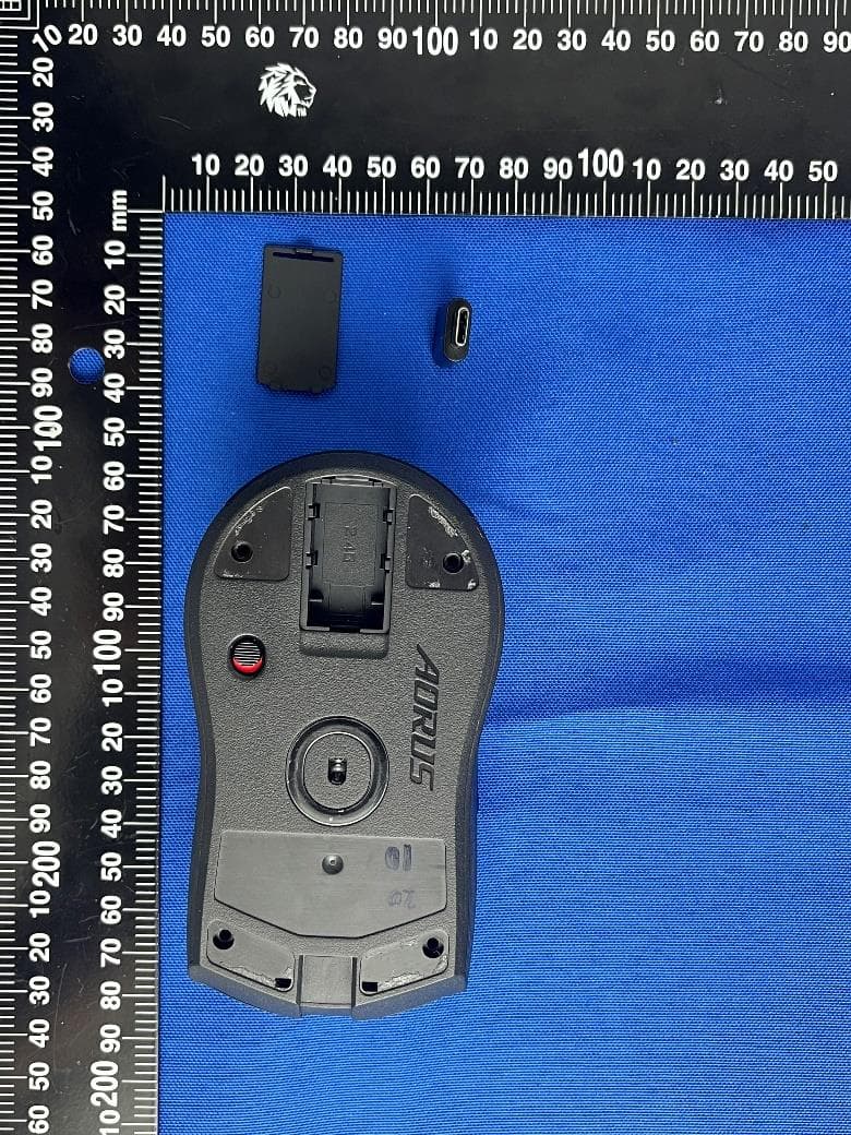
JCKGM-AORUSM6
Jun 26, 2023Mouse
Equipment Class
DTS - Digital Transmission System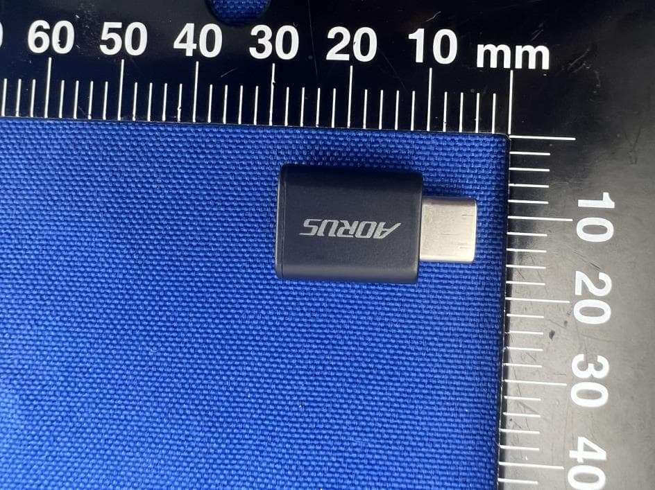
JCKS3
Jun 26, 2023Mouse Dongle
Equipment Class
DTS - Digital Transmission System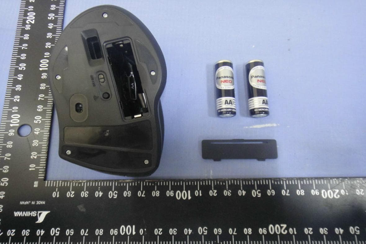
JCK28713AIREM60
Jul 30, 2015Sapphire Blue Optical Mouse
Equipment Class
DXX - Part 15 Low Power Communication Device Transmitter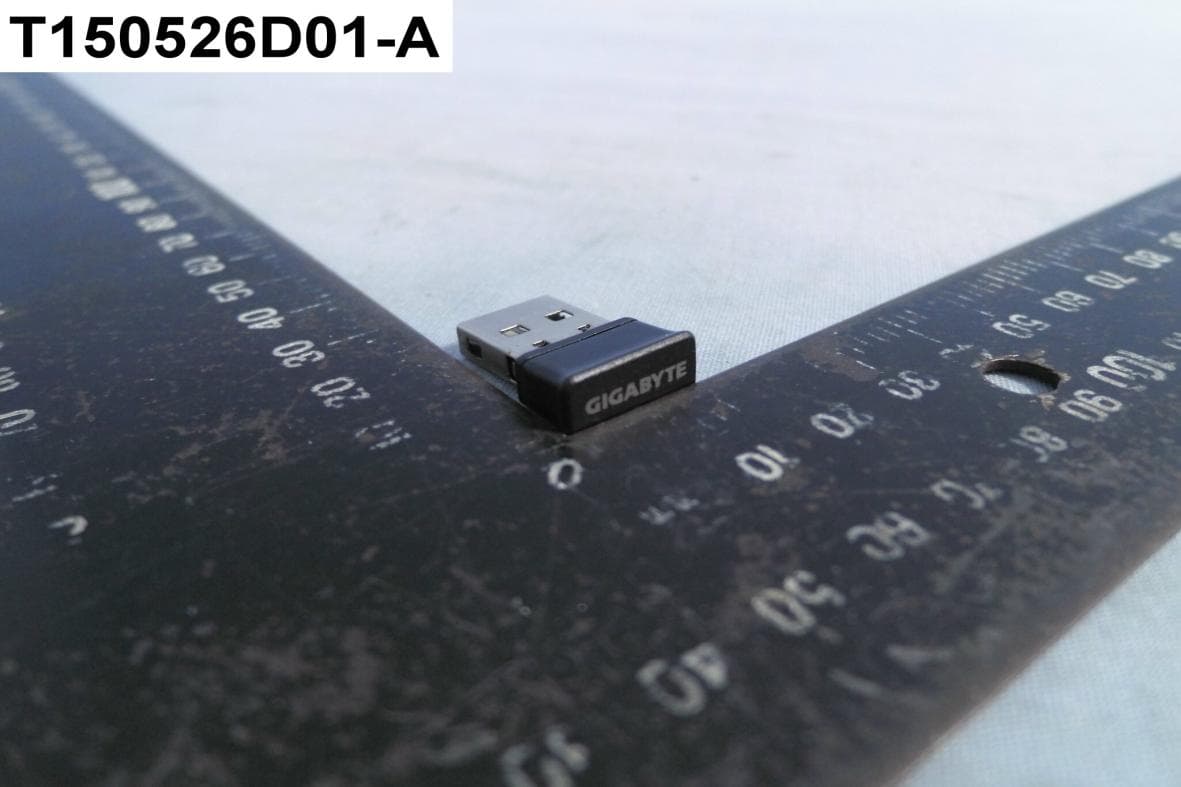
JCK287137580RX
Jul 30, 2015Wireless Receiver
Equipment Class
DXX - Part 15 Low Power Communication Device Transmitter
JCK-MSN09C01
Feb 10, 2015NFC Controller Module with Integrated Antenna
Equipment Class
DXX - Part 15 Low Power Communication Device Transmitter