JCKGN-AP101BWireless Access Point
GIGA-BYTE TECHNOLOGY CO., LTD.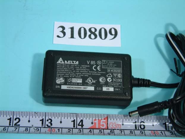
Click to zoom
Application Details
- Equipment Class
- DTS - Digital Transmission System
- Date of Grant
- Jun 16, 2003
- Application Purpose
- Original Equipment
- Date of Application
- Jun 16, 2003
- Equipment Note
- Wireless Access Point
- Frequency Range
- 2412.00000000 - 2462.00000000
- Country
- Taiwan
Documents & Files
Document Text
Text extracted from the exhibit documents filed with the FCC. Open a document above to read the original.
Users Manual
GN-AP101B Wireless Access Point User Guide http://www.gigabyte.com.tw Rev.1.1 Safety, Care and Regulatory Information Important safety instructions Read and follow all instructions marked on the product and in the documentation before you operate your system. Retain all safety and operating instructions for future use. z The product should be operated only from the type of power source indicated on the rating label. z The plug-socket combination must be accessible at all times because it serves as the main disconnecting device. z All products hipped with a three-wire electrical grounding-type plug only fits into a grounding-type power outlet. This is a safety feature. The equipment grounding should be in accordance with local and national electrical codes. The equipment operates safely when it is used in accordance with its marked electrical ratings and product usage instructions z Do not use this product near water or a heat source. z Set up the product on a stable work surface or so as to ensure stability of the system. z Openings in the case are provided for ventilation. Do not block or cover these openings. Make sure you provide adequate space around the system for ventilation when you set up your work area. Never insert objects of any kind into the ventilation openings. z To avoid electrical shock, always unplug all power cables and modem cables from the wall outlets before removing covers. z Allow the product to cool before removing covers or touching internal components. z Use only the power cord and batteries indicated in this manual. Do not dispose of batteries in a fire. They may explode. Check with codes for possible special disposal instructions. Precautions for Products With Modems, Telecommunications, or Local Area Network Options Observe the following guidelines when working with options: • Avoid using a telephone (other than a cordless type) during an electrical storm. There may be a remote risk of electric shock from lightning. • CAUTION - To reduce the risk of fire, use only No. 26 AWG or larger telecommunication line cord. • Do not plug a modem or telephone cable into the network interface controller (NIC) receptacle. • Disconnect the modem cable before opening a product enclosure, touching or installing internal components, or touching an uninsulated modem cable or jack. • Do not use a telephone line to report a gas leak while you are in the vicinity of the leak. • Do not use this product near water, for example, near a bathtub, washbowl, and kitchen sink or laundry tub, in a wet basement or near a swimmin g pool. Federal Communications Commission (FCC) Statement FEDERAL COMMUNICATIONS COMMISSION: This device complies with Part 15 of the FCC Rules. Operation is subject to the following two conditions:(1) this device may not cause harmful interference, and (2) this device must accept any interference received, including interference that may cause undesired operation. Note: This equipment has been tested and found to comply with the limits for a Class B digital device, pursuant to Part 15 of the FCC Rules. These limits are designed to provide reasonable protection. This equipment generates, uses and can radiated radio frequency energy and, if not installed and used in accordance with the instructions, may cause harmful interference to radio communications. However, there is no guarantee that interference will not occur in a particular installation If this equipment does cause harmful interference to radio or television reception, which can be determined by turning the equipment off and on, the user is encouraged to try to correct the interference by one or more of the following measures: • Reorient or relocate the receiving antenna. • Increase the separation between the equipment and receiver. • Connect the equipment into an outlet on a circuit different from that to which the receiver is connected. • Consult the dealer or an experienced radio/TV technician for help. Changes or modifications not expressly approved by the party responsible for compliance could void the user‘s authority to operate the equipment. FCC Radiation Exposure Statement: This equipment complies with FCC radiation exposure limits set forth for an uncontrolled environment. In order to avoid the possibility of exceeding the FCC radio frequency exposure limits, human proximity to the antenna shall not be less than 20cm (8 inches) during normal operation. Proposed RF exposure safety information to include in User’s Manual. / For European users only / European Community Directive Conformance Statement This product is in conformity with the protection requirements of EC Council Low Voltage Directive (Safety) 73/23/EEC, EMC Directive 89/336/EEC on the approximation of the laws of the Member States relating to electro-magnetic compatibility. Contents 1. INTRODUCTION....................................................................................................1 1-1. CONTENTS OF YOUR SHIPMENT...........................................................................1 1-2. PHYSICAL INTERFACE..........................................................................................2 1-3. ACCESS POINT LED INDICATORS.........................................................................2 1-4. KEY FEATURES.....................................................................................................3 1-5. SPECIFICATIONS...................................................................................................3 2. INSTALLATION .....................................................................................................4 3. ACCESS POINT MANAGER ................................................................................7 3-1. INSTALLING THE ACCESS POINT MANAGER.........................................................7 3-2. USING THE ACCESS POINT MANAGER...............................................................12 4. UPGRADE FIRMWARE...............................................…
Text truncated - open the document above for the full version.
Block Diagram
55 44 33 22 11 D D C C B B A A 1.8V 3.3V V1 82100-41 3.3V 802.11b I2 FLASH 3.3V POWER CONSUMPTION PCMCIA W2 SDRAMX2 60mA 1155mW 185mA 198mW 3.3V DEVICEV2W1 ADM6996 350mA 610mW AC101 I1 25mA 105mA205mW90mW 3.3V1.8V 2.5V SDRAM 8MBytes 1.3W 200mW 80mA 170mA 710mA561mW1278mW GPIO-21 PCMCIA_IRQ- GPIO-17GPIO-25 UR_IRQ- GPIO-20 Lan_REST- GPIO-8 Wan_REST- GPIO-05 UR_REST- GPIO-27 BUTTON INIT LED GPIO-18APGPIO-19 State 0State 1 GPIO-26 Wireless GPIO Function Router LEDGPIO-18 State 0 GPIO-24 Wireless POWER 3.3V HCS4- PCMCIA_REST- PCMCIAUR HC10HC9HC8 PCMCIAPCMCIAPCMCIA WaitWriteRead RJ45 CONEXANT LAN4 FLASH SWITCH Network Processor MII RJ45 Host Bus 802.11b Transformer RJ45 Memory Bus MII Wireless Lan LAN3 Transformer LAN1 RJ45LAN2 10/100 Phy. RJ45 2MBytes WAN Port Mac2 Mac1 GN-AP101B 1.0 GN-APb101 C 15 星期一 , 四月 21, 2003 TitleSize Document Number Rev Date: Sheet of
External Photos
FCC ID: JCKGN-AP101B NUMBER 1 FRONT SIDE OF EUT FCC ID: JCKGN-AP101B NUMBER 2 REAR SIDE OF EUT FCC ID: JCKGN-AP101B NUMBER 3 FRONT SIDE OF ADAPTOR FCC ID: JCKGN-AP101B NUMBER 4 REAR SIDE OF ADAPTOR FCC ID: JCKGN-AP101B NUMBER 5 FRONT SIDE OF ADAPTOR
ID Label/Location Info
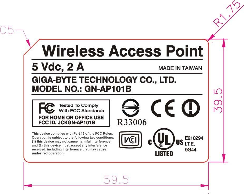
FCC ID: JCKGN-AP101B Label Location
Internal Photos
FCC ID : JCKGN-AP101B Number 1 Mechanical Construction FCC ID : JCKGN-AP101B Number 2 Mechanical Construction FCC ID : JCKGN-AP101B Number 3 Mechanical Construction FCC ID : JCKGN-AP101B Number 4 Front side of Main Board FCC ID : JCKGN-AP101B Number 5 Rear side of Main Board FCC ID : JCKGN-AP101B Number 6 Front side of RF Module FCC ID : JCKGN-AP101B Number 7 Rear side of RF Module FCC ID : JCKGN-AP101B Number 8 Mechanical Construction of RF Module FCC ID : JCKGN-AP101B Number 9 Mechanical Construction of RF Module FCC ID : JCKGN-AP101B Number 10 Mechanical Construction of RF Module FCC ID : JCKGN-AP101B Number 11 Front side of Main Board of RF Module FCC ID : JCKGN-AP101B Number 12 Rear side of Main Board of RF Module
Operational Description
FCC ID: JCKGN-AP101B Operational Description The NEC Point-M main board is using the IDT RC32332 Microprocessor, which is 32bits, and 133Mhz. About this CPU processor is using 2 * SDRAM interface 2M * 4Banks * 16 bits SDRAM. Totally is about 32M byte. The local bus interface is using 2M byte Flash RAM. One PCI interface is using Via6105 Rhin fast Ethernet controller to RJ45 LAN port, And the other one PCI interface is using TI1410A, which are high performance PCI to PC card controller. The PCI bus supports Single PC card socket compliant with the wireless LAN card. The wireless LAN card module is made up of the IEEE 802.11b MAC, Baseband, and radio components, PCMCIA interface, two mmcx connectors for external antenna. It uses direct sequence spread spectrum (DSSS) technology and implements DBPSK, DQPSK, and CCK modulation. This provides a very robust radio channel and excellent receiver sensitivity. With its PCMCIA Type-II extended form factor, low power consumption, power management and high-speed wireless data communication, it is ideally suited for integration into mobile and handheld platform.
Schematics
55 44 33 22 11 D D C C B B A A LAYOUT NOTE: PLACE A 470pF IN PAR ALLEL WITH EACH 0.1uF 196FPBGA READY RemovedInstalled ROM BOOTFLASH BOOT Boot Jumper Options: (GPIO37) (UART IRQ) UARTINT ARM_DRAM_Flash_UART 0.1V GN-APb101 C 25 星期一 , 四月 21, 2003 TitleSize Document Number Rev Date: Sheet of R_MD0R_MD4 HCS_ R_MD2 MRAS# HAD21 R_MCLKR_MM1R_MCS# HC0 CLKI R_MD9R_MWE# HAD29HAD16 R_MD5 BCLKIO MA6MA7 R_MD1 HAD22 R_MD13 PLLBP R_MCKE BOOTSEL_ R_MD6R_MM0 MA9 HAD18 GPIO27 HAD19 MCAS# R_MD11R_MD8 MA1 R_MD10R_MD7 HAD27HAD25 MA3 HAD26 MA8 HAD24 R_MD3 HAD28 GPIO25 R_MD15R_MD14R_MD12 BOOTSEL_ HRST_ HAD6HAD2HAD0 HAD3HRST_ HC1 HAD5HRD- HAD4 HAD1 GPIO25 HWR-HC3 MD4 MA9MA11MM0MA10 MD0MD12 MA1MA0MCS#MCAS#MM1MA2 MD14MD15 MCKEMRAS# MD6 MB0MA5MA8 MD9MD5 MA7MA4MB1 MD13MD7 MA3 MD8MD2 MCLK MD10MD11 MWE#MA6 MD1MD3 MA11MA4MA5MA0MA2MA10MCKEMM0MCS#MWE#MCLKMM1 GPIO27 HC2HAD22HAD21HC1 HRD- HC5HC4HAD18HAD17HAD26HAD25HC3HC6HC7HAD16HAD19HAD20HAD23HAD24 HWR-HCS_ HRST_HAD28HAD27HAD29 HAD6HAD4HAD5HAD1HAD15HAD13HAD8HAD12HAD10HAD14HAD2HAD3HAD9HAD7HAD0HAD11 HC7HAD4HAD9HAD8 HWR- HAD6 HRD- HC4HC1HAD10HC3HC2HC5HC6HAD11HAD5HAD7HAD12HAD14 WAIT- HAD0HAD3HAD2HAD1HAD13HAD17HAD15 HRST_ TST0 HAD31 HAD7HC2 R_MD1R_MD5R_MD12R_MD14R_MD0R_MD8R_MD2R_MD13R_MD9R_MD11R_MD3R_MD15R_MD6 MB1MB0 TST2TST1TST3 CLKI HAD23HAD20 R_MD10R_MD4R_MD7 MD2MD7MD9MD11MD3MD1MD8MD13MD10MD14MD0MD15MD5MD12MD6MD4 HCS4- 5 USBN 5USBP 5 25CLK1 3 RST_W 5W_LED 5L_RST- 3S0 5S1 5 HRST_ HAD16 5 HAD19 5 HC5 5 HC4 5 HC7 5 HRD- 5 HC2 5 HC3 5 HC1 5 HWR- 5 WAIT- 5 HC6 5 HAD17 5 HAD14 5 HAD15 5 HAD13 5 HAD12 5 HAD9 5 HAD11 5 HAD10 5 HAD3 5 HAD1 5 HAD6 5 HAD8 5 HAD4 5 HAD5 5 HAD7 5 HAD2 5 HAD0 5 UART CS_ 5 IRQ_W- 5W_RST- 4 HAD20 5 M2_RXD3 4 M2_TXD2 4 RXCLK2 4 M2_TXD3 4 M2_RXDV 4 M2_TXER 4 M2_RXD2 4 M2_TXD1 4 M2_CRS 4 M2_TXD0 4 M2_COL 4 M2_RXD0 4 M2_RXD1 4 TXCLK2 4 M2_TXEN 4 M1_TXD0 3 MDC1 3 M1_RXD3 3 M1_TXER 3 M1_TXD3 3 M1_TXD2 3 M1_TXD1 3 M1_COL 3 M1_TXEN 3 TXCLK1 3 M1_RXDV 3 M1_RXD2 3 M1_CRS 3 RXCLK1 3 MDIO1 3 M1_RXD0 3 M1_RXD1 3 RXER1 3 Wap_Led 5 V18 VCC3 VCC3 VCC3 V18 VCC3 VCC3 VCC3 VCC3 VCC3 VCC3 VCC3 VCC3 VCC3 VCC3 VCC3 VCC3 VCC3 V18 SRN18P4R-22/S 1357 2468 R20 33/6 SRN28P4R-22/S 1357 2468 SRN38P4R-22/S 1357 2468 SRN48P4R-22/S 1357 2468 R5 51/6 C221uF/8 Y1 35.328MHz 4 12 3 VCC OE GND OUT R4 51/6 SR135 1K/6/S C110.1uF/6 R2410K/6 C1822pF/6 D1 LED_GREEN/X C70.1uF/6 SFB2FB80/8/S R7 51/6 R8 51/6 C30.1uF/6 C330.1uF/6 C21 0.1uF/6 C80.1uF/6 C340.1uF/6 C170.1uF/6 R190/6/X C50.1uF/6 U3 CX82100-41 J1J5 J8 B1C3 H10 C4 E2 E1 F2F1 D1 A5 E3 G2G1G5 H7 G7 H6 A2 H4 G6H5J2J3 J4 K2 J6 K1K3K5 D14 D8 K4 L3L1 M2M1 N2N1 M3 F6 D12 N3 P3 M4 N4 P4 L4 M5 L5 F9 F4 M6 K6 N6 P6 L6 P7 N7 H8 G8 M7 M9 F12 G9 L8 K9 J9 N10 P10 M10 L9 K10 B5 H11 L10 M11 J10 L11 N12 P12 J7 K13 P14 M12M13 N14 N13 B9 J14H12H13J11H14 K7 L2 G13G12H9G14G10F13G11F14 K11 N8 F10E13F11E14E12E10E11D13 N5 P2 C13C14B14B13C12A13B12D11 N9 P5 C11F8A11C10D10B10E9A10 N11 P9 A9C9D9E8A8 A12 B11 E6D6 P1 P11 E5D5C5B4A4D4 B3 P13 A3B2A1G4C6 K8 M8 H3H1H2 L7 P8 F5F3 E4 G3 C1C2D2D3 L13 M14 K12 L12L14 K14 B8 J12 B6A6 C8 A14 A7B7E7 C7D7 J13 F7 GPIO39 (FCLKIO) BCLKIO HAD31 GPIO20GPIO21 VDDO VSSO I2C DATA EM1_TX_CLKEM1_TXD0EM1_TX_EN VDDO VSSO I2C CLOCK EM1_CRSEM1_COLEM1_RX_CLK VDD VSS VGG GPIO18 EM1_RXD0 VDDA VSSA CLKI PLLBP TRST#TCKTMSTDITDOTREQA VDDO VSSO GPIO14 (BOPT) HAD29HAD28HAD27HAD26HAD25HAD24HAD23 VDDO VSSO HAD22HAD21HAD20HAD19HAD18HAD17HAD16HC07 VDDO VSSO HC06HC05HC04HC03HC02HC01HAD15 VDD VSS GPIO25 HAD14 VDDO VSSO HAD13HAD12HAD11HAD10HAD09HAD08HAD07HAD06 VDDO VSSO HAD05HAD04HAD03HAD02HAD01HAD00 VDDO VSSO HC10HC09HC08HRST# VSSO VSS0 MD15MD14MD13MD12MD11 VDDO VSSO MD10MD09MD08MD07MD06MD05MD04MD03 VDDO VSS0 MD02MD01MD00 MCLK MCKE MM1MM0 MRAS# VDDO VSSO MCAS# MCS# MWE# MA11MA10MA09MA08MA07 VDDO VSSO MA06MA05MA04MA03MA02MA01MB01MA00 VDDO VSSO MB00 GPIO22 (USB Pwr Det) USBP USBN GPIO26 VDDO VSS0 GPIO5GPIO6 VDDO VSSO GPIO7 (LED_READY) GPIO8 TST0TST1TST2TST3 VDDO HC00 GPIO17GPIO19GPIO24GPIO27GPIO31 EM1_MDCEM1_MDIOEM1_RXD1EM1_RXD2EM1_RXD3EM1_RXDVEM1_RXEREM1_TXD1EM1_TXD2EM1_TXD3EM1_TXER NCNCNCNC EM2_TX_CLKEM2_TXD0EM2_TXD1EM2_TXD2EM2_TXD3EM2_TXEREM2_COLEM2_CRSEM2_MDCEM2_MDIOEM2_RX_CLKEM2_RXD0EM2_RXD1EM2_RXD2EM2_RXD3EM2_RXDVEM2_RXEREM2_TX_EN NC C350.1uF/6 SR16 1K/6/X/S R140/6 C360.1uF/6 J2 H_2X10 1 4 5379 11 2681012 13151719 14161820 R610K/6 FB1FB80/8 C370.1uF/6 C380.1uF/6 C320.1uF/6 R210/6/X C60.1uF/6 TP1 T POINT A 1 C10.1uF/6 SR12 1K/6/S U2AM29LV16 2524232221201918 87654321 481128261214 9 293133353840424430323436394143451337472746 17161510 A0A1A2A3A4A5A6A7A8A9A10A11A12A13A14A15A16WE#OE#CE#RESET# (RP#)WP#NC D0D1D2D3D4D5D6D7D8D9 D10D11D12D13D14D15 Vpp/NC Vcc VccQ/BYTE# GNDGND A17A18A19/RDYA20/NC SC150.1uF/6/S SW1PUSHBUTTON 1 24 3 J1 H_1X2 12 C1922pF/6 R10 220/6/X C23470pF/6 R230/6 C10 0.01uF/6 R17 51/6 C24470pF/6 SC420.1uF/6/S C40.1uF/6 C25470pF/6 R1 10K/6 R9 220/6 C90.1uF/6 U1 Micron_SDRAM_8MB 2324252629303132333422201817161938373915 245781011134244454748505153 1 27 3 9 43 49 28 54 6 12 46 52 3521 1441 A0A1A2A3A4A5A6A7A8A9A10BA0RAS#CAS#WE#CS#CLKCLKEDQMHDQML DQ0DQ1DQ2DQ3DQ4DQ5DQ6DQ7DQ8DQ9 DQ10DQ11DQ12DQ13DQ14DQ15 Vdd Vdd VddQ VddQ VddQ VddQ Vss Vss VssQ VssQ VssQ VssQ A11BA1 VddVss R131K/6 C26470pF/6 R15 51/6 R3 51/6 SC160.1uF/6/S C270.1uF/6 R224.7K/6 R2 51/6 C28470pF/6 55 44 33 22 11 D D C C B B A A 2KV Phy. Address==01110 WAN When LF8563removeC49,C50,R44,R45 When H1102removeC46,R35 When Routerremove R134 AP use 2.5V When AP removeR136 When AP removeR137 0.1V GN-APb101 C 35 星期一 , 四月 21, 2003 TitleSize Document Number Rev Date: Sheet of TX+ TX- RX+ COL- PDOWN PADD3 RX- MII RXDV-REPEATER PADD2 PADD2 SD ISOLATE ANEN TX- REPEATER PADD0 PLL PADD4 VCC3_IN V25_OUT PADD1PADD3 SPD100 PADD4 RST- RXDV-SPD100 RBIAD ANEN RST- VCC3_IN PADD0 FDUPLEX TX+ COL- FDUPLEX V25_OUT 25M_IN GND_CHASSIS RXP GND_CHASSIS GND_CHASSIS RX+RX- TXPTXMRXM ISOLATEMII PADD1 BURNIN# PDOWNBURNIN# BURNIN# SDRBIAD PLL MDIO1 2 M1_CRS 2 MDC1 2 M1_TXEN 2 M1_COL 2 RXCLK1 2 M1_RXD2 2 M1_RXDV 2 M1_RXD3 2 TXCLK1 2 M1_RXD1 2 M1_RXD0 2 WAN_LINK_ACT- 4 L_RST- 2 M1_TXER 2 RXER1 2 25CLK1 2 GND_CHASSIS 4 M1_TXD1 2 M1_…
Text truncated - open the document above for the full version.
Test Report
FCC TEST REPORT Report No. : F310809 SPORTON International Inc. TEL : 886-2-2696-2468 FAX : 886-2-2696-2255 FCC TEST REPORT for 47 CFR, Part 15, Subpart C Equipment : Wireless Access Point Model No. : GN-AP101B FCC ID : JCKGN-AP101B Filing Type : Certification Applicant : GIGA-BYTE TECHNOLOGY CO., LTD. No. 6, Bau Chiang Road, Hsin-Tien, Taiepi Hsien, Taiwan, R.O.C. The test result refers exclusively to the test presented test model / sample. Without written approval of SPORTON International Inc., the test report shall not be reproduced except in full. Certificate or Test Report must not be used by the applicant to claim the product in this test report endorsement by NVLAP or any agency of U.S. government. SPORTON International Inc. 6F, No.106, Sec. 1, Hsin Tai Wu Rd., Hsi Chih, Taipei Hsien, Taiwan, R.O.C. FCC TEST REPORT Report No. : F310809 SPORTON International Inc. FCC ID : JCKGN-AP101B TEL : 886-2-2696-2468 Page No. : i FAX : 886-2-2696-2255 Issued Date : May 10, 2003 Table of Contents History of this test report..................................................................................................................ii CERTIFICATE OF COMPLIANCE........................................................................................................................1 1. General Description of Equipment under Test.............................................................................................2 1.1. Applicant..........................................................................................................................................................................................2 1.2. Manufacturer ...................................................................................................................................................................................2 1.3. Basic Description of Equipment under Test ....................................................................................................................................2 1.4. Feature of Equipment under Test ...................................................................................................................................................3 2. Test Configuration of Equipment under Test ...............................................................................................4 2.1. Test Manner ....................................................................................................................................................................................4 2.2. Description of Test System .............................................................................................................................................................4 2.3. Connection Diagram of Test System ..............................................................................................................................................6 3. Operation of Equipment under Test ..............................................................................................................7 4. General Information of Test............................................................................................................................8 4.1. Test Voltage ....................................................................................................................................................................................8 4.2. Standard for Methods of Measurement...........................................................................................................................................8 4.3. Test in Compliance with ..................................................................................................................................................................8 4.4. Frequency Range Investigated .......................................................................................................................................................8 4.5. Test Distance ..................................................................................................................................................................................8 5. Report of Measurements and Examinations ................................................................................................9 5.1. List of Measurements and Examinations ........................................................................................................................................9 5.2. 6dB Bandwidth ..............................................................................................................................................................................10 5.3. Peak Output Power .......................................................................................................................................................................14 5.4. Power Spectral Density .................................................................................................................................................................15 5.5. Test of Conducted Emission .........................................................................................................................................................19 5.6. Test of Radiated Emission ............................................................................................................................................................23 5.7. Band Edges Measurement............................................................................................................................................................32 5.8. Antenna Requirements .................................................................................................................................................................35 5.9. RF Exposure .....................................................................................................................................…
Text truncated - open the document above for the full version.
Test Setup Photos
FCC TEST REPORT Report No.: F310809 SPORTON International Inc. FCC ID : JCKGN-AP101B TEL : 886-2-2696-2468 Page No. : 1 of 3 FAX : 886-2-2696-2255 Issued Date : May 10, 2003 1.1. Photographs of Conducted Emission Test Configuration The photographs show the configuration that generates the maximum emission. FRONT VIEW REAR VIEW FCC TEST REPORT Report No.: F310809 SPORTON International Inc. FCC ID : JCKGN-AP101B TEL : 886-2-2696-2468 Page No. : 2 of 3 FAX : 886-2-2696-2255 Issued Date : May 10, 2003 SIDE VIEW FCC TEST REPORT Report No.: F310809 SPORTON International Inc. FCC ID : JCKGN-AP101B TEL : 886-2-2696-2468 Page No. : 3 of 3 FAX : 886-2-2696-2255 Issued Date : May 10, 2003 1.2. Photographs of Radiated Emission Test Configuration The photographs show the configuration that generates the maximum emission. FRONT VIEW REAR VIEW
Contact Information
Applicant
Alain Sam-Lai
Test Firm
SPORTON International IncKathy Lin
Technical Specifications
| # | Rule Parts | Frequency Range | Power Output |
|---|---|---|---|
| 1 | 15C | 2.41 GHz - 2.46 GHz | 20.00 mW |
Other Applications from GIGA-BYTE TECHNOLOGY CO., LTD.
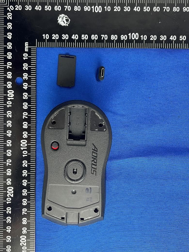
JCKGM-AORUSM6
Jun 26, 2023Mouse
Equipment Class
DTS - Digital Transmission System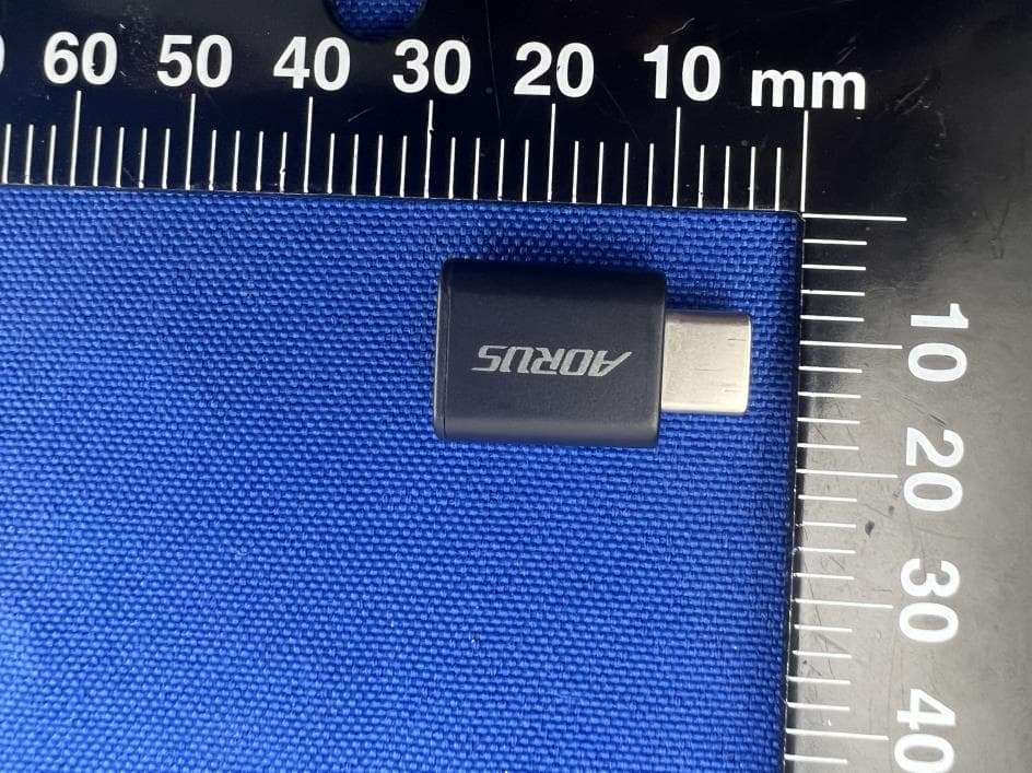
JCKS3
Jun 26, 2023Mouse Dongle
Equipment Class
DTS - Digital Transmission System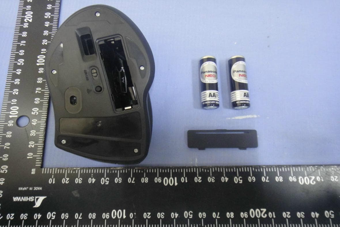
JCK28713AIREM60
Jul 30, 2015Sapphire Blue Optical Mouse
Equipment Class
DXX - Part 15 Low Power Communication Device Transmitter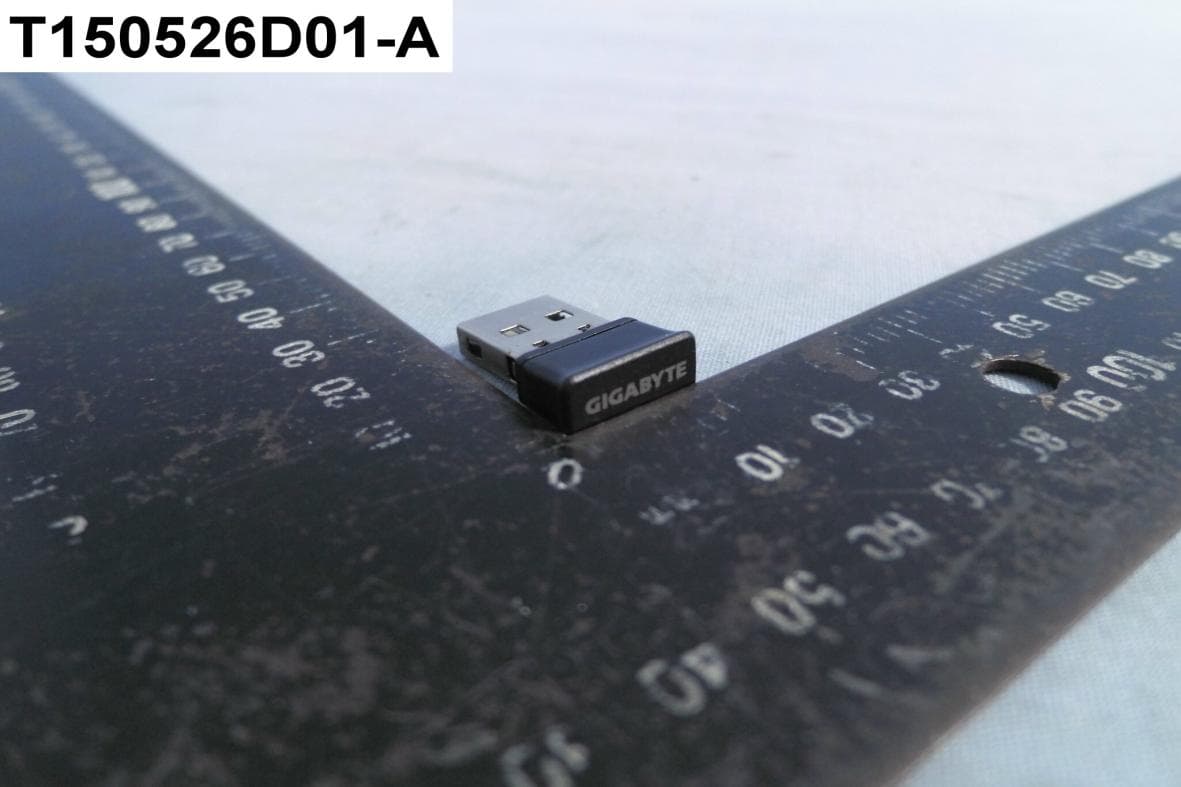
JCK287137580RX
Jul 30, 2015Wireless Receiver
Equipment Class
DXX - Part 15 Low Power Communication Device Transmitter
JCK-MSN09C01
Feb 10, 2015NFC Controller Module with Integrated Antenna
Equipment Class
DXX - Part 15 Low Power Communication Device Transmitter