JYCGB210Triple Band GSM850/DCS1800/PCS1900 (with WAP&GPRS)
Pantech Co Ltd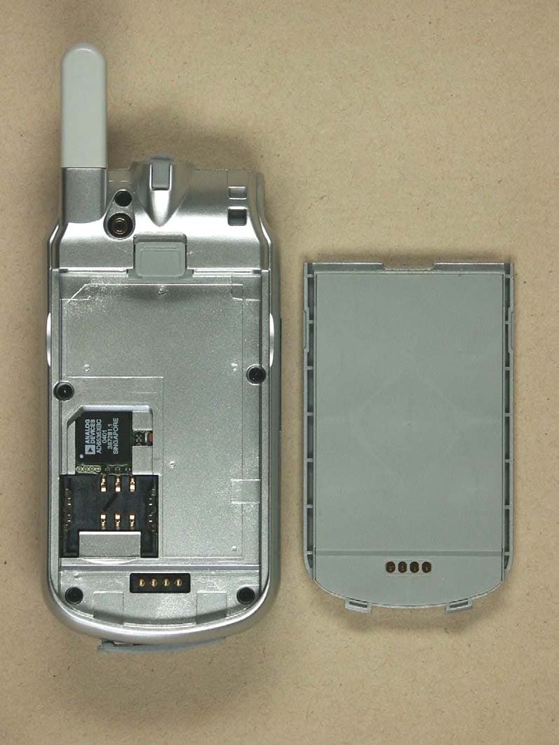
Click to zoom
Application Details
- Equipment Class
- PCE - PCS Licensed Transmitter held to ear
- Date of Grant
- Aug 18, 2004
- Application Purpose
- Original Equipment
- Date of Application
- Aug 18, 2004
- Equipment Note
- Triple Band GSM850/DCS1800/PCS1900 (with WAP&GPRS)
- Frequency Range
- 824.20000000 - 848.80000000
- Company
- Pantech Co Ltd
- Country
- South Korea
Documents & Files
Document Text
Text extracted from the exhibit documents filed with the FCC. Open a document above to read the original.
Block Diagram
π/2 Φ DET I Q Q I AFC CLK VCTCXO 13 MHz SILAB SI4205
Cover Letter(s)
Pantech Co., Ltd. Sinsong Center Bldg. 6th Fl., 25-12,Yeouido-dong, Yeoungdeungpo-gu, Seoul, Korea Tel.: +82-2-3660-5862 Fax: +82-2-3660-5990 ______________________________________________________________________ LETTER OF AUTHORIZATION DATE : July 19, 2004 To whom it may concern: We the undersigned, hereby authorize ETS Germany to act on our behalf in all manners relating to application for equipment authorization, including signing of all documents relating to these matters. Any and all acts carried out by ETS Germany on our behalf shall have the same affect as acts of our own. This authorization is valid until further written notice from Pantech Co., Ltd. Sincerely, (Company counsel or company officer signature) (Name and Title)
Cover Letter(s)
Pantech Co., Ltd. Sinsong Center Bldg. 6th Fl., 25-12,Yeouido-dong, Yeoungdeungpo-gu, Seoul, Korea Tel.: +82-2-3660-5862 Fax: +82-2-3660-5990 ______________________________________________________________________ Date : 2004. 07. Federal Communications Commission Equipment Authorization Branch 7435 Oakland Mills Road Columbia, MD 21046 Request for Confidentiality Pantech Co., Ltd. FCC ID: JYCGB210 Gentlemen, In accordance with 0.459 of CFR 47, Pantech Co., Ltd. hereby requests confidentiality of all Schematics, Parts List, attachments for the subject application. These documents contain detailed system and equipment description and related information about the product which Pantech Co., Ltd. considers to be proprietary, confidential and a custom design and otherwise would not release to the general public. Since the design is a basis from which future technological products will evolve, Pantech Co., Ltd. considers that this information would be of benefit to its competitors and that the disclosure of the information in these documents would give competitors an unfair advantage in the market. Sincerely, Name : Byung-Wan Kim Title : Senior Manager Company : Pantech Co., Ltd.
External Photos
ELECTRONIC TECHNOLOGY SYSTEMS DR.GENZ GMBH ETS Dr. Genz GmbH, Germany Registration number: G5M204040055-P-2224 Page 1 of 12 Appendix A. Pictures ELECTRONIC TECHNOLOGY SYSTEMS DR.GENZ GMBH ETS Dr. Genz GmbH, Germany Registration number: G5M204040055-P-2224 Page 2 of 12 ELECTRONIC TECHNOLOGY SYSTEMS DR.GENZ GMBH ETS Dr. Genz GmbH, Germany Registration number: G5M204040055-P-2224 Page 3 of 12 ELECTRONIC TECHNOLOGY SYSTEMS DR.GENZ GMBH ETS Dr. Genz GmbH, Germany Registration number: G5M204040055-P-2224 Page 4 of 12 ELECTRONIC TECHNOLOGY SYSTEMS DR.GENZ GMBH ETS Dr. Genz GmbH, Germany Registration number: G5M204040055-P-2224 Page 5 of 12
ID Label/Location Info
Pantech Co., Ltd. Sinsong Center Bldg. 6th Fl., 25-12,Yeouido-dong, Yeoungdeungpo-gu, Seoul, Korea Tel.: +82-2-3660-5862 Fax: +82-2-3660-5990 ______________________________________________________________________ [Label Location] Description: Triple Band GSM 850/DCS 1800/PCS 1900 (with WAP & GPRS) FCC ID: JYCGB210
ID Label/Location Info
Pantech Co., Ltd. Sinsong Center Bldg. 6th Fl., 25-12,Yeouido-dong, Yeoungdeungpo-gu, Seoul, Korea Tel.: +82-2-3660-5862 Fax: +82-2-3660-5990 ______________________________________________________________________ [FCC ID Label sample] Description: Triple Band GSM 850 / DCS1800 / PCS 1900 (with WAP & GPRS) FCC ID: JYCGB210
Internal Photos
ELECTRONIC TECHNOLOGY SYSTEMS DR.GENZ GMBH ETS Dr. Genz GmbH, Germany Registration number: G5M204040055-P-2224 Page 6 of 12 ELECTRONIC TECHNOLOGY SYSTEMS DR.GENZ GMBH ETS Dr. Genz GmbH, Germany Registration number: G5M204040055-P-2224 Page 7 of 12 ELECTRONIC TECHNOLOGY SYSTEMS DR.GENZ GMBH ETS Dr. Genz GmbH, Germany Registration number: G5M204040055-P-2224 Page 8 of 12
Operational Description
Pantech Co., Ltd. Sinsong Center Bldg. 6th Fl., 25-12,Yeouido-dong, Yeoungdeungpo-gu, Seoul, Korea Tel.: +82-2-3660-5862 Fax: +82-2-3660-5990 ______________________________________________________________________ Declaration concerning Antenna Specification It’s hereby declared that the product: ............ GB210.................... fulfills the requirement in FCC test relating to the antenna type. The ............GB210.............confirm to FCC recommendation with External-Fixed antenna type: (model if applicable) GB210 has a unique connector gain of the antenna +0.77(peak)... dBi frequency range ... 824 to 893, 1710 to 1890, 1850 to 1990.......MHz. : please refer to the below The mounting of the antenna is fixed to the radio module and no other antenna should be used. Company: Pantech Co., Ltd. City: Seoul ZIP / Postal code: 150-745 Country: Korea Place: KOREA Date: July 19, 2004
Operational Description
GB210 Service Manual GB210 GB210 Service Manual (GSM Cellular Phone) Pantech Co., Ltd., Korea July 19, 2004 1 st Edition For Use by Authorized Service/Maintenance Personal Only Documents to Receive This Addendum: GB210 Maintenance/Repair/Operating Manual GB210 Service Manual PANTECH R&D CONFIDENTIAL 1 CONTENTS SECTION 1 INTRODUCTION .............................................................................................................3 1.1 INTRODUCTION..............................................................................................................................3 1.2 FREQUENCY ALLOCATION AND ITS USE...........................................................................................3 1.3 ITEM NAME AND USE......................................................................................................................4 1.4 CHARACTERISTICS.........................................................................................................................4 SECTION 2 ELECTRICAL SPECIFICATIONS....................................................................................5 2.1 GENERAL......................................................................................................................................5 2.2 TRANSMITTER..........................................................................................................5 2.3 RECEIVER...............................................................................................................5 SECTION 3 OPERATION....................................................................................................................6 3.1 NAME OF EACH PART...................................................................................................6 3.2.DISPLAY ..................................................................................................................7 3.3 KEYPAD ................................................................................................................7 SECTION 4 THEORY OF OPERATION..............................................................................................8 4.1 LOGIC SECTION ........................................................................................................................8 4.1.1 DC DISTRIBUTION AND REGULATION PART......................................................................8 4.1.2 LOGIC PART..........................................................................................................8 4.1.2.1 SUMMARY..........................................................................................................9 4.1.2.2 BASEBAND DIGITAL SIGNAL PROCESSING...................................................................10 4.1.3 MEMORY PART.....................................................................................................12 4.1.4 NOTIFICATION PART..................................................................................................................13 4.1.5 KEY PAD PART..........................................................................................................................13 4.1.6 LCD MODULE(DISPLAY PART)...................................................................................................13 4.2 RADIO TRANSCEIVER SECTION.....................................................................................................14 4.2.1 DC DISTRIBUTION AND REGULATION PART.................................................................................15 4.2.2 TRANSCEIVER PIN DESCRIPTION.......................................................................15 4.2.3 RECEIVE SECTION.................................................................................................17 4.2.3.1 AN OVERVIEW OF RECEIVE SECTION.......................................................................................17 4.2.3.2 RECEIVER PART.................................................................................................18 4.2.4 TRANSMIT SECTION..................................................................................................................19 4.2.4.1 AN OVERVIEW OF TRANSMIT SECTION....................................................................................19 4.2.4.2 TRANSMITTER PART...............................................................................................................20 4.2.5 OFFSET PLL.........................................................................................................22 4.2.5.1 AN OVERVIEW OF OFFSET PLL ............................................................................................22 4.2.5.2 VCTCXO(VOLTAGE CONTROLLED TEMPERATURE COMPENSATED CRYSTAL OSCILLATOR):V801....23 SECTION 5 ALIGNMENT PROCEDURE..........................................................................................24 5.1 RECOMMENDED TEST EQUIPMENT................................................................................................24 5.2 CONNECTION OF TEST EQUIPMENT...............................................................................................24 SECTION 6 EQUIPMENT REPAIR PROCEDURE ...........................................................................25 6.1 NO POWER ON WITH BATTERY APPLIED..........................................................................................25 6.1.1 POWER CHECK.........................................................................................................................25 6.1.2 OSCILLATION CHECK ................................................................................................................28 6.1.3 KEYPAD LED NOT IN OPERATION...............................................................................................29 6.1.4 STATUS LED ................................................................................................. ...30 6.2 AUDIO PART(EARPIECE, HANDS FREE EARPHONE, MICROPHONE, HA…
Text truncated - open the document above for the full version.
Parts List/Tune Up Info
Pantech Co., Ltd. Sinsong Center Bldg. 6th Fl., 25-12,Yeouido-dong, Yeoungdeungpo-gu, Seoul, Korea Tel.: +82-2-3660-5862 Fax: +82-2-3660-5990 __________________________________________________________________________________ Date: 2004. 07 Federal Communications Commission Equipment Authorization Branch 7435 Oakland Mills Road Columbia, MD 21046 Declaration – Tuning Procedure Pantech Co., Ltd. FCC ID: JYCGB210 FCC Part 2, 24 Certification Gentlemen, There are no user accessible adjustments or tuning for this Triple Band GSM 850 / DCS1800 / PCS 1900 (with WAP & GPRS). All necessary adjustments and tuning are performed during manufacture of the product. Sincerely, Byung-Wan Kim Senior Manager Pantech Co., Ltd.
RF Exposure Info
ETS Dr. Genz GmbH, Germany Registration number: G5M204040055-S-8 Appendix B ELECTRONIC TECHNOLOGY SYSTEMS DR.GENZ GMBH Appendix B Measurement Plots Date/Time: 05/05/04 11:46:10 Test Laboratory: ELECTRONIC TECHNOLOGY SYSTEMS DR. GENZ GMBH Dipol Valid.900(m)_250mW_05.05.2004 DUT: Dipole 900 MHz; Type: D900V2; Serial: 164 Communication System: CW; Frequency: 900 MHz;Duty Cycle: 1:1 Medium: Muscle 900 MHz Medium parameters used: f = 900 MHz; σ = 1.04 mho/m; ε r = 54.4; ρ = 1000 kg/m 3 Phantom section: Flat Section DASY4 Configuration: z Probe: ET3DV6 - SN1711; ConvF(6, 6, 6); Calibrated: 12/16/2003 z Sensor-Surface: 4mm (Mechanical And Optical Surface Detection) z Electronics: DAE3 Sn522; Calibrated: 1/12/2004 z Phantom: SAM 12; Type: TP-1217; Serial: QD000P40CA z Measurement SW: DASY4, V4.2 Build 44; Postprocessing SW: SEMCAD, V1.8 Build 112 Dipol 900 (250mW)/Area Scan (51x81x1): Measurement grid: dx=15mm, dy=15mm Reference Value = 56.8 V/m; Power Drift = -0.1 dB Maximum value of SAR (interpolated) = 3.18 mW/g Dipol 900 (250mW)/Zoom Scan (7x7x7)/Cube 0: Measurement grid: dx=5mm, dy=5mm, dz=5mm Reference Value = 56.8 V/m; Power Drift = -0.1 dB Maximum value of SAR (measured) = 3.1 mW/g Peak SAR (extrapolated) = 4.11 W/kg SAR(1 g) = 2.86 mW/g; SAR(10 g) = 1.88 mW/g 0 dB = 3.1mW/g Date/Time: 05/06/04 07:04:09 Test Laboratory: ELECTRONIC TECHNOLOGY SYSTEMS DR. GENZ GMBH Dipol Valid.900(h)_250mW_06.05.2004 DUT: Dipole 900 MHz; Type: D900V2; Serial: 164 Communication System: CW; Frequency: 900 MHz;Duty Cycle: 1:1 Medium: Head 900 MHz Medium parameters used (interpolated): f = 900 MHz; σ = 0.958 mho/m; ε r = 41.3; ρ = 1000 kg/m 3 Phantom section: Flat Section DASY4 Configuration: z Probe: ET3DV6 - SN1711; ConvF(6.2, 6.2, 6.2); Calibrated: 12/16/2003 z Sensor-Surface: 4mm (Mechanical And Optical Surface Detection) z Electronics: DAE3 Sn522; Calibrated: 1/12/2004 z Phantom: SAM 12; Type: TP-1217; Serial: QD000P40CA z Measurement SW: DASY4, V4.2 Build 44; Postprocessing SW: SEMCAD, V1.8 Build 112 Dipol 900 (250mW)/Area Scan (51x81x1): Measurement grid: dx=15mm, dy=15mm Reference Value = 59.4 V/m; Power Drift = -0.0 dB Maximum value of SAR (interpolated) = 3.09 mW/g Dipol 900 (250mW)/Zoom Scan (7x7x7)/Cube 0: Measurement grid: dx=5mm, dy=5mm, dz=5mm Reference Value = 59.4 V/m; Power Drift = -0.0 dB Maximum value of SAR (measured) = 3 mW/g Peak SAR (extrapolated) = 4.06 W/kg SAR(1 g) = 2.58 mW/g; SAR(10 g) = 1.66 mW/g 0 dB = 3mW/g Date/Time: 05/06/04 08:21:19 Test Laboratory: ELECTRONIC TECHNOLOGY SYSTEMS DR. GENZ GMBH 850_right_ch128_cheek DUT: Triple Band GSM 850 (E-GSM) / DCS 1800 / PCS 1900 (with WAP & GPRS); Type: ---; Serial: GB210 Communication System: GSM 850; Frequency: 824.2 MHz;Duty Cycle: 1:8.3 Medium: Head 850 MHz Medium parameters used (interpolated): f = 824.2 MHz; σ = 0.892 mho/m; ε r = 42.2; ρ = 1000 kg/m 3 Phantom section: Right Section DASY4 Configuration: z Probe: ET3DV6 - SN1711; ConvF(6.2, 6.2, 6.2); Calibrated: 12/16/2003 z Sensor-Surface: 4mm (Mechanical And Optical Surface Detection) z Electronics: DAE3 Sn522; Calibrated: 1/12/2004 z Phantom: SAM 12; Type: TP-1217; Serial: QD000P40CA z Measurement SW: DASY4, V4.2 Build 44; Postprocessing SW: SEMCAD, V1.8 Build 112 GB210/Area Scan (91x161x1): Measurement grid: dx=10mm, dy=10mm Reference Value = 7.83 V/m; Power Drift = 0.0 dB Maximum value of SAR (interpolated) = 1.45 mW/g GB210/Zoom Scan (7x7x7)/Cube 0: Measurement grid: dx=5mm, dy=5mm, dz=5mm Reference Value = 7.83 V/m; Power Drift = 0.0 dB Maximum value of SAR (measured) = 1.45 mW/g Peak SAR (extrapolated) = 1.89 W/kg SAR(1 g) = 1.32 mW/g; SAR(10 g) = 0.851 mW/g 0 dB = 1.45mW/g Date/Time: 05/06/04 10:31:14 Test Laboratory: ELECTRONIC TECHNOLOGY SYSTEMS DR. GENZ GMBH 850_right_ch128_tilted DUT: Triple Band GSM 850 (E-GSM) / DCS 1800 / PCS 1900 (with WAP & GPRS); Type: ---; Serial: GB210 Communication System: GSM 850; Frequency: 824.2 MHz;Duty Cycle: 1:8.3 Medium: Head 850 MHz Medium parameters used (interpolated): f = 824.2 MHz; σ = 0.892 mho/m; ε r = 42.2; ρ = 1000 kg/m 3 Phantom section: Right Section DASY4 Configuration: z Probe: ET3DV6 - SN1711; ConvF(6.2, 6.2, 6.2); Calibrated: 12/16/2003 z Sensor-Surface: 4mm (Mechanical And Optical Surface Detection) z Electronics: DAE3 Sn522; Calibrated: 1/12/2004 z Phantom: SAM 12; Type: TP-1217; Serial: QD000P40CA z Measurement SW: DASY4, V4.2 Build 44; Postprocessing SW: SEMCAD, V1.8 Build 112 GB210/Area Scan (91x161x1): Measurement grid: dx=10mm, dy=10mm Reference Value = 11.3 V/m; Power Drift = 0.0 dB Maximum value of SAR (interpolated) = 0.626 mW/g GB210/Zoom Scan (7x7x7)/Cube 0: Measurement grid: dx=5mm, dy=5mm, dz=5mm Reference Value = 11.3 V/m; Power Drift = 0.0 dB Maximum value of SAR (measured) = 0.620 mW/g Peak SAR (extrapolated) = 0.769 W/kg SAR(1 g) = 0.581 mW/g; SAR(10 g) = 0.401 mW/g 0 dB = 0.620mW/g Date/Time: 05/06/04 07:42:01 Test Laboratory: ELECTRONIC TECHNOLOGY SYSTEMS DR. GENZ GMBH 850_right_ch189_cheek DUT: Triple Band GSM 850 (E-GSM) / DCS 1800 / PCS 1900 (with WAP & GPRS); Type: ---; Serial: GB210 Communication System: GSM 850; Frequency: 836.4 MHz;Duty Cycle: 1:8.3 Medium: Head 850 MHz Medium parameters used (interpolated): f = 836.4 MHz; σ = 0.883 mho/m; ε r = 42.3; ρ = 1000 kg/m 3 Phantom section: Right Section DASY4 Configuration: z Probe: ET3DV6 - SN1711; ConvF(6.2, 6.2, 6.2); Calibrated: 12/16/2003 z Sensor-Surface: 4mm (Mechanical And Optical Surface Detection) z Electronics: DAE3 Sn522; Calibrated: 1/12/2004 z Phantom: SAM 12; Type: TP-1217; Serial: QD000P40CA z Measurement SW: DASY4, V4.2 Build 44; Postprocessing SW: SEMCAD, V1.8 Build 112 GB210/Area Scan (91x161x1): Measurement grid: dx=10mm, dy=10mm Reference Value = 7.21 V/m; Power Drift = -0.1 dB Maximum value of SAR (interpolated) = 1.22 mW/g GB210/Zoom Scan (7x7x7)/Cube 0: Measurement grid: dx=5mm, dy=5mm, dz=5mm Reference Value = 7.21 V/m; Power Drift = -0.1 dB Maximum value of SAR (measured) = 1.2 mW/g Peak SAR (extrapolated) = 1.48 W/kg SAR(1 …
Text truncated - open the document above for the full version.
Test Setup Photos
ELECTRONIC TECHNOLOGY SYSTEMS DR.GENZ GMBH ETS Dr. Genz GmbH, Germany Registration number: G5M204040055-P-2224 Page 9 of 12 ELECTRONIC TECHNOLOGY SYSTEMS DR.GENZ GMBH ETS Dr. Genz GmbH, Germany Registration number: G5M204040055-P-2224 Page 10 of 12 ELECTRONIC TECHNOLOGY SYSTEMS DR.GENZ GMBH ETS Dr. Genz GmbH, Germany Registration number: G5M204040055-P-2224 Page 11 of 12 ELECTRONIC TECHNOLOGY SYSTEMS DR.GENZ GMBH ETS Dr. Genz GmbH, Germany Registration number: G5M204040055-P-2224 Page 12 of 12
Contact Information
Applicant
Bum-Young Lee(Vice President)
Test Firm
Eurofins Product Service GmbHRobert Kschiwan-Kaspar
Technical Specifications
| # | Rule Parts | Frequency Range | Power Output | Emission | Tolerance |
|---|---|---|---|---|---|
| 2 | 22H | 824.2 MHz - 848.8 MHz | 906.00 mW | 253KGXW | 1 ppm |
Other Applications from Pantech Co Ltd
JYCP2050
Aug 04, 2013GSM/WCDMA Phone with Bluetooth
Equipment Class
PCE - PCS Licensed Transmitter held to ear
JYCORBIT
Feb 19, 2013CDMA/PCS,GSM,WCDMA,LTE Portable Router with WLAN
Equipment Class
PCB - PCS Licensed Transmitter
JYCPREMIAV
Sep 06, 2012CDMA/GSM/LTE Phone with BT/WLAN/NFC
Equipment Class
DTS - Digital Transmission System
JYCCDMAPTL21
Aug 29, 2012GSM/WCDMA/CDMA Phone with Bluetooth/WLAN/NFC
Equipment Class
DSS - Part 15 Spread Spectrum Transmitter
JYCSPARKLE
Aug 21, 2012CDMA/GSM/EDGE/WCDMA/LTE USB Data Dongle
Equipment Class
PCB - PCS Licensed Transmitter