K37JC9957VGA Card
Jace Tech Inc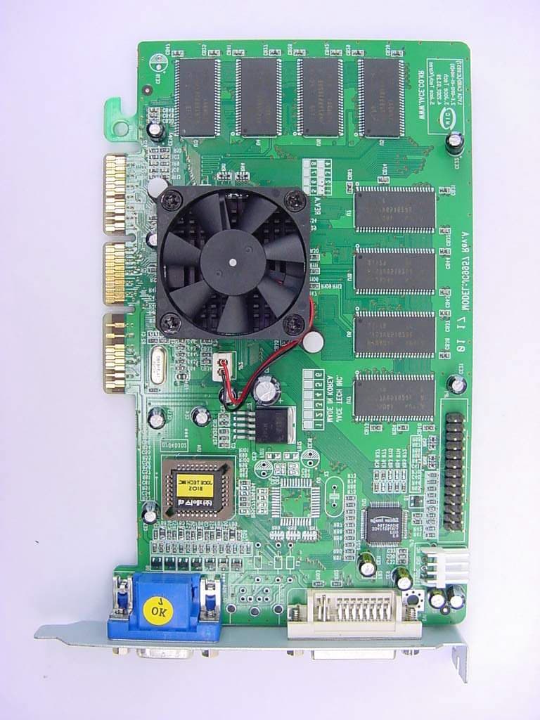
Click to zoom
Application Details
- Equipment Class
- JBP - Part 15 Class B Computing Device Peripheral
- Date of Grant
- Oct 17, 2001
- Application Purpose
- Original Equipment
- Date of Application
- Oct 17, 2001
- Equipment Note
- VGA Card
- Company
- Jace Tech Inc
- Country
- South Korea
Documents & Files
Document Text
Text extracted from the exhibit documents filed with the FCC. Open a document above to read the original.
Users Manual
NVIDIA Geforce2 MX400 Graphics Accelerator JC9957 User’s Guide JACE TECH INC. FCC NOTICE This device complies with part 15 of the FCC Rules. Operation is subject to the following two conditions: (1) This device may not cause harmful interface, and (2) This device must accept any interference received, including interference that may cause undesired operation. INFORMATION TO THE USER This eq uip me nt has be e n tes ted a nd fo und to co mp ly with the limits fo r a C las s B d igita l de vice, p urs ua nt to Pa rt 15 o f FCC Rules. The se limits a re des igned to pro vide rea so nab le p rotec tio n a ga inst harmful interfere nce in re s ide ntia l ins ta llatio n. This equipment generates, uses and can radiate radio frequency energy and, if not installed and used in accordance with the instructions, may cause harmful interference to radio communications. However, there is no guarantee that interference will not occur in particular installation. If this equipment does cause interference to radio or television reception, which can be determined by turning the equipment off and on, the user is encouraged to try to correct the interference by one or more of the following measures: • Reorient or relocate the receiving antenna. • Increase the separation between the equipment and receiver. • Connect the equipment into an outlet on a circuit different from that to with the receiver is connected. • Consult the dealer or an experienced radio/TV technician for help and for additional suggestions. The user may find the following booklet prepared by Federal Communications Commiss io n he lp ful: "How to ide ntify a nd Resolve Radio-TV Interference Problems." This booklet is available from the U.S. Government Printing O ffice, Washington, DC 20402, Stock No. 004-000-00345-4. FCC WARNING The user is cautioned that changes or modifications not expressly approved by the manufacturer could void the user's authority to operate this equipment. Note :In o rder fo r a n insta lla tio n o f this p rod uct to ma inta in co mp lia nce with the limits fo r a C lass B de vice, s hie lded cab les must be used. NOTICE The information in this document is subject to change in order to improve reliability, design, or function without prior notice and does no t rep rese nt a co mmitme nt o n the part o f this co mpa ny. In no e ve nt will we b e liab le fo r d irect, ind ire ct, spec ia l, inc ide nta l, or conseq ue ntia l da ma ges a ris ing o ut o f the use o r the inab ility to use the prod uc t or doc ume nta tio n, e ve n if ad vised o f the poss ib ility o f s uc h da ma ges. No part o f this re fere nce ma nua l ma y be reprod uced o r tra ns mitted in a ny form o r b y a ny mea ns witho ut the p rio r writte n permis s io n o f this co mpa ny. TRADEMARK ACKNOWLEDGMENTS Microsoft , Microsoft Word, and Microsoft Windows are registered trademarks of Microsoft Corp. Multiscan is a trademark of Sony Corporation of America. MultiSync is a trademark of NEC Home Electronics (USA) Inc. Geforce2 MX400 is registered trademarks of N VIDIA Corporation. All other product names or trademarks are property of their respective owners. Table of Content Introduction.....................................................................................................1 1.1 Features .....................................................................................................1 1.2 Board Configuration.................................................................................1 Installing Drivers for Windows 98 ................................................................2 User’s Guide 1 Introduction 1.1 Features This ma nua l pro vide s opera ting instructio ns for user utilities a nd insta lla tio n instructio ns fo r the d isp la y d rive rs s upp lied. This grap hic s s ys te m is VGA co mpa tib le. The utilities a nd d rive rs s upp lied with yo ur vga ca rd pro vide s upport for additional features, such as greater speed, higher resolution, and more available colors. ! Supports AGP 2X/4X mode ! Built- in a high pe rforma nce H/W 3 D se tup e ngine ! Supports 4MX16 DDR SDRAM types up to 166 MHz ! Built- in pro gra mmab le 24-b it true-co lor RAMDAC up to 350MHz pixel clock ! Supports super high resolution graphics modes - 640x480 256/32K/64K/16M colors at 85Hz NI - 800x600 16/256/32K/64K/16M colors at 85Hz NI - 1024x768 16/256/32K/64K/16M colors at 85Hz NI - 1280x1024 16/256/32K/64K/16M colors at 85 Hz NI - 1600x1200 16/256/32K/64K/16M colors at 85 Hz NI ! Supports VESA Display Power Management Signaling (DPMS) compliant VGA monitor for power management ! Supports DDC1 and DDC2B specifications 1.2 Board Configuration JC9957 Installing Drivers 2 Installing Drivers for Windows 98 1. After Windo ws has loaded, select Settings on the Start menu. 2. Select Co nt rol Pa ne l on the Se ttings menu and click on the Display icon. 3. The Display Properties window appears. Select the Se ttings tab and click on the Advanced b utto n. User’s Guide 3 4. From the next window select Adapte r tab and click on the Change button. 5. Update Device Driver Wizard window appears. C lick on the Next butto n to co ntinue the ins ta llatio n. 6. Select Search for a better driver than the one your device is using now and click on the Next button. Installing Drivers 4 7. In the Specify a location: box, enter the location of the Vanta graphics accelerator drivers and click on the Next button. (D: is the CD-ROM d rive inc lud ing drive r files. ) 8. When the refreshed window appears. C lick on the Next button. User’s Guide 5 9. Click o n the Fi nis h b utto n to co ntinue the insta lla tio n. 10. To finis h s ett ing up yo ur ne w hard ware, yo u mus t res tart yo ur co mp uter. W he n S yste m Sett ings C ha nge w indo w appears, click on the Ye s button.
External Photos
FCC ID.: K37JC9957 File No.: E01OR-001 ONETECH Testing & Evaluation Lab.
ID Label/Location Info
FCC ID. : K37JC9957 File No. : E01OR-001 ONETECH Testing & Evaluation Lab . IDENTIFICATION LABEL: PROPOSED FCC ID LABEL The label included following statement will be attached on the top right side of product. This device complies with Part 15 of the FCC Rules. Operation is subject to the following two conditions: (1) this device may not cause harmful interference, and (2) this device must accept any interference received, including interference that may cause undesired operations. Made in Korea FCC ID : K37JC9957 ΦΧΧ Ι∆
Internal Photos
FCC ID.: K37JC9957 File No.: E01OR-001 ONETECH Testing & Evaluation Lab.
Test Report
Page 1 of 13 FCC ID.: Error! Unknown docume nt prope rty name . File No.: Error! Unknown docume nt prope rty name . This report shall not be reproduced except in full without our written approval.FCC-004 (Rev.0) HEAD OFFICE : #505 SK APT. Factory 223-28, Sangdaewon 1 Dong, Jungwon- Gu, Seongnam- C ity, K yunggi- Do, 462-121, Korea (TEL: +82- 31-746-8500 FAX: +82-31-746-8700 ) EM C Te s ting De pt : 426-1 Daessangryung- Ri, C howol- Myun, K wangju- Si, K yunggi- Do, 464-860 Korea. (TEL: +82- 31-765-8289 FAX: +82-31-766-2904) ONETECH Testing & Evaluation Lab . ELECTROMAGNETIC EMISSION COMPLIANCE REPORT FOR FCC CLASS B CERTIFICATION Test report file number : E01OR-001 Applicant : JACE TECH INC. A ddre s s: 9th Floor, Hyundae O ffice , 9-4 Soonae -Dong, Bundang-Ku, Se ongnam City, Kyungki-Do, Ko re a Manufacture r : JACE TECH INC. A ddre s s: 9th Floor, Hyundae O ffice , 9-4 Soonae -Dong, Bundang-Ku, Se ongnam City, Kyungki-Do, Ko re a Type of Equipme nt : VG A Card FCC ID: K37JC9957 Model / Type No. : JC9957 Serial number: JC15DM957G-00214 Total page of Report: 13 pages (including this page) Date of Incoming: Sep 26, 2001 Date of issuing : October 4, 2001 SUMMARY The equipment complies with the regulation; FCC PART 15 CFR 47 SUBPART B, Class B. This test report contains only the result of a single test of the sample supplied for the examination. It is not a general valid assessment of the features of the respective products of the mass-production. Page 2 of 13 FCC ID.: Error! Unknown docume nt prope rty name . File No.: Error! Unknown docume nt prope rty name . This report shall not be reproduced except in full without our written approval.FCC-004 (Rev.0) HEAD OFFICE : #505 SK APT. Factory 223-28, Sangdaewon 1 Dong, Jungwon- Gu, Seongnam- C ity, K yunggi- Do, 462-121, Korea (TEL: +82- 31-746-8500 FAX: +82-31-746-8700 ) EM C Te s ting De pt : 426-1 Daessangryung- Ri, C howol- Myun, K wangju- Si, K yunggi- Do, 464-860 Korea. (TEL: +82- 31-765-8289 FAX: +82-31-766-2904) ONETECH Testing & Evaluation Lab . Reviewed by: Approved by: Y. K. Nam / Assist. Chief EngineerY. K. Kwon / Chief Engineer EMC Dept.EMC Dept. ONETECH Corp.ONETECH Corp. Page 3 of 13 FCC ID.: Error! Unknown docume nt prope rty name . File No.: Error! Unknown docume nt prope rty name . This report shall not be reproduced except in full without our written approval.FCC-004 (Rev.0) HEAD OFFICE : #505 SK APT. Factory 223-28, Sangdaewon 1 Dong, Jungwon- Gu, Seongnam- C ity, K yunggi- Do, 462-121, Korea (TEL: +82- 31-746-8500 FAX: +82-31-746-8700 ) EM C Te s ting De pt : 426-1 Daessangryung- Ri, C howol- Myun, K wangju- Si, K yunggi- Do, 464-860 Korea. (TEL: +82- 31-765-8289 FAX: +82-31-766-2904) ONETECH Testing & Evaluation Lab . CONTENTS Page 1. VERIFICATION OF COMPLIANCE ................................................................................................................ 4 2. GENERAL INFORMATION .................................................................................................................................. 5 2.1 P RODUCT D ESCRIPTION ............................................................................................................................................. 5 2.2 R ELATED S UBMITTAL ( S ) / G RANT ( S ) ...................................................................................................................... 5 2.3 T EST S YSTEM D ETAILS .............................................................................................................................................. 6 2.4 T EST M ETHODOLOGY ................................................................................................................................................ 6 2.5 T EST F ACILITY ............................................................................................................................................................ 6 3. SYSTEM TEST CONFIGURATION ................................................................................................................... 7 3.1 J USTIFICATION ............................................................................................................................................................. 7 3.2 EUT EXERCISE S OFTWARE ........................................................................................................................................ 7 3.3 C ABLE D ESCRIPTION .................................................................................................................................................. 7 3.4 N OISE S UPPRESSION P ARTS ON C ABLE ................................................................................................................... 8 3.5 E QUIPMENT M ODIFICATIONS .................................................................................................................................... 8 3.6 C ONFIGURATION OF T EST S YSTEM .......................................................................................................................... 8 4. PRELIMINARY TEST .............................................................................................................................................. 9 4.1 C ONDUCTED E MISSION T EST .................................................................................................................................... 9 4.2 R ADIAT ED E MISSION T EST ........................................................................................................................................ 9 5. FINAL RESULT OF MEASURMENT ............................................................................................................. 10 5.1 C ONDUCTED E MISSION T EST .................................................................................................................................. 10 6. FIELD STRENGTH CALCULATION ..........................................................................................................…
Text truncated - open the document above for the full version.
Test Setup Photos
FCC ID.: K37JC9957 File No.: E01OR-001 ONETECH Testing & Evaluation Lab . FCC ID.: K37JC9957 File No.: E01OR-001 ONETECH Testing & Evaluation Lab .
Contact Information
Applicant
Cha Jae Won(President)
Test Firm
ONETECH Corp.Y. Kwon
Technical Specifications
| # | Rule Parts | Frequency Range | Power Output |
|---|---|---|---|
| 1 | 15B | - | - |
Other Applications from Jace Tech Inc
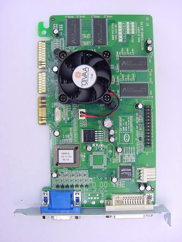
K37JC9960
Oct 17, 2001VGA Card
Equipment Class
JBP - Part 15 Class B Computing Device PeripheralK37JC9232
Jan 25, 1996Video Board Maximum resolution: 1280 X 1024 NI
Equipment Class
JBP - Part 15 Class B Computing Device PeripheralK37JC9234
Aug 24, 1995PCI Video Card Maximum resolution: 1280 X 1024 interlaced.
Equipment Class
JBP - Part 15 Class B Computing Device PeripheralK37JC9230K
Jul 16, 1995PCI Video Card Maximum resolution: 1280 X 1024 interlaced.
Equipment Class
JBP - Part 15 Class B Computing Device PeripheralK37JC9230K4
Apr 23, 1995PCI VGA Card(1280 X 1024 Interlaced.
Equipment Class
JBP - Part 15 Class B Computing Device Peripheral