K37JC9960VGA Card
Jace Tech Inc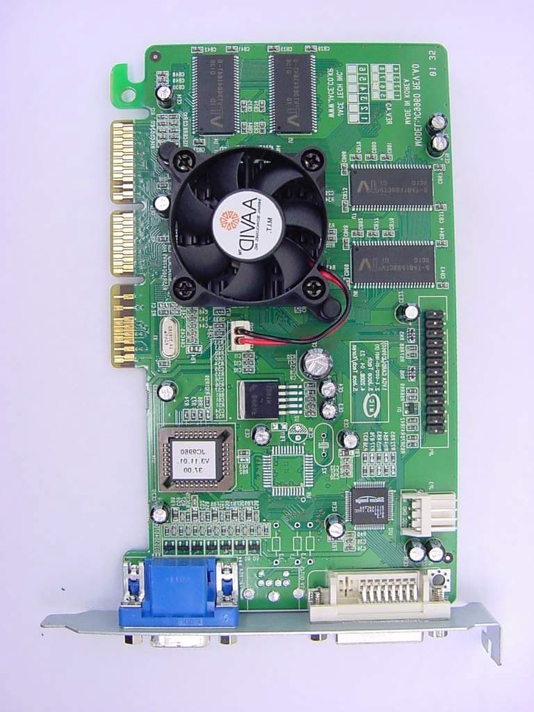
Click to zoom
Application Details
- Equipment Class
- JBP - Part 15 Class B Computing Device Peripheral
- Date of Grant
- Oct 17, 2001
- Application Purpose
- Original Equipment
- Date of Application
- Oct 17, 2001
- Equipment Note
- VGA Card
- Company
- Jace Tech Inc
- Country
- South Korea
Documents & Files
Document Text
Text extracted from the exhibit documents filed with the FCC. Open a document above to read the original.
Users Manual
NVIDIA Geforce2 MX200 Graphics Accelerator JC9960 User’s Guide FCC NOTICE This device complies with part 15 of the FCC Rules. Operation is subject to the following two conditions: (1) This device may not cause harmful interface, and (2) This device must accept any interference received, including interference that may cause undesired operation. INFORMATION TO THE USER This equipment has been tested and found to comply with the limits for a Class B digital device, pursuant to Part 15 of FCC Rules. These limits are designed to provide reasonable protection against harmful interference in residential installation. This equipment generates, uses and can radiate radio frequency energy and, if not i nstalled and used in accordance with the instructions, may cause harmful i nterference to radio communications. However, there is no guarantee that interference will not occur in particular installation. If this equipment does cause i nterference to radio or television reception, which can be determi ned by turni ng the equipment off and on, the user is encouraged to try to correct the interference by one or more of the followi ng measures: • Reorient or relocate the receivi ng antenna. • Increase the separation between the equipment and receiver. • Connec t the equipme nt into a n o utle t o n a circuit differe nt from that to with the recei ver is co nnected . • Consult the dealer or an experienced radio/TV technician for help and for additional suggestions. The user may find the followi ng booklet prepared by Federal Communications Commission helpful: "How to identify and Resolve Radio-TV Interference Problems." This booklet is available from the U.S.Government Pri nti ng Office, Washington, DC 20402, Stock No. 004-000-00345-4. FCC WARNING The user is cautioned that changes or modifications not expressly approved by the manufacturer could void the user's authority to operate this equipment. Note: In order for an installation of this product to maintain compliance with the limits for a Class B device, shielded cables must be used. NOTICE The information in this document is subject to change i n order to improve reliability, design, or function without prior notice and does not represent a commitment on the part of this company. In no event will we be liable for direct, indirect, special, i ncidental, or consequential damages arising out of the use or the i nability to use the product or documentation, even if advised of the possibility of such damages. No part of this reference manual may be reproduced or transmitted in any form or by any means without the prior written permission of this company. TRADEMARK ACKNOWLEDGMENTS Microsoft, Microsoft Word, and Microsoft Wi ndows are registered trademarks of Microsoft Corp. Multiscan is a trademark of Sony Corporation of America. MultiSync is a trademark of NEC Home Electronics (USA) Inc. Geforce2 MX200 is registered trademarks of NVID IA Corporation. All other product names or trademarks are property of their respective o wners. Table of Content Introduction.....................................................................................................1 1.1 Features .....................................................................................................1 1.2 Board Configuration.................................................................................1 Installing Drivers for Windows 98 ................................................................2 User’s Guide 1 Introduction 1.1 Features This manual provides operating instructions for user utilities and i nstallation i nstructions for the display drivers supplied. This graphics system is VGA compatible. The utilities and dri vers supplied with your vga card provide support for additional features, such as greater speed, higher resolution, and more available colors. ! Supports AGP 2X/4X mode ! Built-i n a high performance H/W 3D setup engi ne ! Supports 4MX16 DDR SDRAM types up to 166 MHz ! Built-i n programmable 24-bit true-color RAMDAC up to 350MHz pi xel clock ! Supports super high resolution graphics modes - 640x480 256/32K/64K/16M colors at 85Hz NI - 800x600 16/256/32K/64K/16M colors at 85Hz NI - 1024x768 16/256/32K/64K/16M colors at 85Hz NI - 1280x1024 16/256/32K/64K/16M colors at 85 Hz NI - 1600x1200 16/256/32K/64K/16M colors at 85 Hz NI ! Supports VESA Display Power Management Signaling (DPMS) compliant VGA monitor for power management ! Supports DDC1 and DDC2B specifications 1.2 Board Configuration JC9960 Installing Drivers 2 Installing Drivers for Windows 98 1. After Wi ndows has loaded, select Settings on the Start me nu. 2. Select Control Panel on the Settings menu and click on the Display icon. 3. The Display Properties window appears. Select the Settings tab and click on the Advanced button. User’s Guide 3 4. From the next window select Adapter tab and click on the Change butto n. 5. Update Device Driver Wizard window appears. Click on the Next button to continue the i nstallation. 6. Select Search for a better driver than the one your device is using now and click on the Next butto n. Installing Drivers 4 7. In the Specify a location: box, enter the location of the Vanta graphics accelerator drivers and click on the Next button. (D: is the CD-ROM dri ve i ncluding dri ver files.) 8. When the refreshed window appears. C lick on the Next butto n. User’s Guide 5 9. Click on the Finish button to continue the installation. 10. To finish setting up your new hardware, you must restart your computer. When System Settings C hange wi ndow appears, click on the Yes button. Installing Drivers 6
External Photos
FCC ID.: K37JC9960 File No.: E01OR-005 ONETECH Testing & Evaluation Lab.
ID Label/Location Info
FCC ID. : K37JC9960 File No. : E01OR-005 ONETECH Testing & Evaluation Lab . IDENTIFICATION LABEL: PROPOSED FCC ID LABEL The label included following statement will be attached on the top right side of product. This device complies with Part 15 of the FCC Rules. Operation is subject to the following two conditions: (1) this device may not cause harmful interference, and (2) this device must accept any interference received, including interference that may cause undesired operations. Made in Korea FCC ID : K37JC9960 ΦΧΧ Ι∆
Internal Photos
FCC ID.: K37JC9960 File No.: E01OR-005 ONETECH Testing & Evaluation Lab.
Test Report
Page 1 of 13 FCC ID.: Error! Unknown docume nt prope rty name . File No.: Error! Unknown docume nt prope rty name . This report shall not be reproduced except in full without our written approval.FCC-004 (Rev.0) HEAD OFFICE : #505 SK APT. Factory 223-28, Sangdaewon 1 Dong, Jungwon- Gu, Seongnam- C ity, K yunggi- Do, 462-121, Korea (TEL: +82- 31-746-8500 FAX: +82-31-746-8700 ) EM C Te s ting De pt : 426-1 Daessangryung- Ri, C howol- Myun, K wangju- Si, K yunggi- Do, 464-860 Korea. (TEL: +82- 31-765-8289 FAX: +82-31-766-2904) ONETECH Testing & Evaluation Lab . ELECTROMAGNETIC EMISSION COMPLIANCE REPORT FOR FCC CLASS B CERTIFICATION Test report file number : E01OR-005 Applicant : JACE TECH INC. A ddre s s: 9th Floor, Hyundae O ffice , 9-4 Soonae -Dong, Bundang-Ku, Se ongnam City, Kyungki-Do, Ko re a Manufacture r : JACE TECH INC. A ddre s s: 9th Floor, Hyundae O ffice , 9-4 Soonae -Dong, Bundang-Ku, Se ongnam City, Kyungki-Do, Ko re a Type of Equipme nt : VG A Card FCC ID: K37JC9960 Model / Type No. : JC9960 Se rial numbe r: None Total page of Report: 13 pages (including this page) Date of Incoming: Sep 26, 2001 Date of issuing : October 4, 2001 SUMMARY The equipment complies with the regulation; FCC PART 15 CFR 47 SUBPART B, Class B. This test report contains only the result of a single test of the sample supplied for the examination. It is not a general valid assessment of the features of the respective products of the mass-production. Page 2 of 13 FCC ID.: Error! Unknown docume nt prope rty name . File No.: Error! Unknown docume nt prope rty name . This report shall not be reproduced except in full without our written approval.FCC-004 (Rev.0) HEAD OFFICE : #505 SK APT. Factory 223-28, Sangdaewon 1 Dong, Jungwon- Gu, Seongnam- C ity, K yunggi- Do, 462-121, Korea (TEL: +82- 31-746-8500 FAX: +82-31-746-8700 ) EM C Te s ting De pt : 426-1 Daessangryung- Ri, C howol- Myun, K wangju- Si, K yunggi- Do, 464-860 Korea. (TEL: +82- 31-765-8289 FAX: +82-31-766-2904) ONETECH Testing & Evaluation Lab . Reviewed by: Approved by: Y. K. Nam / Assist. Chief EngineerY. K. Kwon / Chief Engineer EMC Dept.EMC Dept. ONETECH Corp.ONETECH Corp. Page 3 of 13 FCC ID.: Error! Unknown docume nt prope rty name . File No.: Error! Unknown docume nt prope rty name . This report shall not be reproduced except in full without our written approval.FCC-004 (Rev.0) HEAD OFFICE : #505 SK APT. Factory 223-28, Sangdaewon 1 Dong, Jungwon- Gu, Seongnam- C ity, K yunggi- Do, 462-121, Korea (TEL: +82- 31-746-8500 FAX: +82-31-746-8700 ) EM C Te s ting De pt : 426-1 Daessangryung- Ri, C howol- Myun, K wangju- Si, K yunggi- Do, 464-860 Korea. (TEL: +82- 31-765-8289 FAX: +82-31-766-2904) ONETECH Testing & Evaluation Lab . CONTENTS Page 1. VERIFICATION OF COMPLIANCE ................................................................................................................ 4 2. GENERAL INFORMATION .................................................................................................................................. 5 2.1 P RODUCT D ESCRIPTION ............................................................................................................................................. 5 2.2 R ELATED S UBMITTAL ( S ) / G RANT ( S ) ...................................................................................................................... 5 2.3 T EST S YSTEM D ETAILS .............................................................................................................................................. 6 2.4 T EST M ETHODOLOGY ................................................................................................................................................ 6 2.5 T EST F ACILITY ............................................................................................................................................................ 6 3. SYSTEM TEST CONFIGURATION ................................................................................................................... 7 3.1 J USTIFICATION ............................................................................................................................................................. 7 3.2 EUT EXERCISE S OFTWARE ........................................................................................................................................ 7 3.3 C ABLE D ESCRIPTION .................................................................................................................................................. 7 3.4 N OISE S UPPRESSION P ARTS ON C ABLE ................................................................................................................... 8 3.5 E QUIPMENT M ODIFICATIONS .................................................................................................................................... 8 3.6 C ONFIGURATION OF T EST S YSTEM .......................................................................................................................... 8 4. PRELIMINARY TEST .............................................................................................................................................. 9 4.1 C ONDUCTED E MISSION T EST .................................................................................................................................... 9 4.2 R ADIAT ED E MISSION T EST ........................................................................................................................................ 9 5. FINAL RESULT OF MEASURMENT ............................................................................................................. 10 5.1 C ONDUCTED E MISSION T EST .................................................................................................................................. 10 6. FIELD STRENGTH CALCULATION ............................................................................................................. 16 7. …
Text truncated - open the document above for the full version.
Test Setup Photos
FCC ID.: K37JC9960 File No.: E01OR-005 ONETECH Testing & Evaluation Lab . FCC ID.: K37JC9960 File No.: E01OR-005 ONETECH Testing & Evaluation Lab .
Contact Information
Applicant
Cha Jae Won(President)
Test Firm
ONETECH Corp.Y. Kwon
Technical Specifications
| # | Rule Parts | Frequency Range | Power Output |
|---|---|---|---|
| 1 | 15B | - | - |
Other Applications from Jace Tech Inc
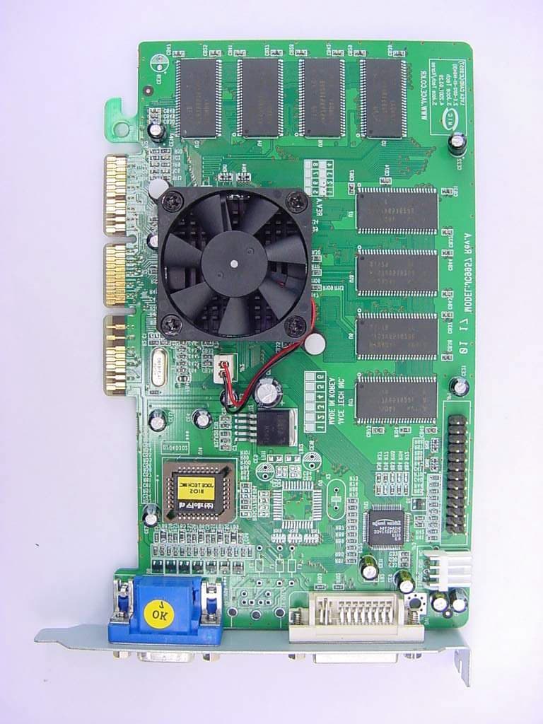
K37JC9957
Oct 17, 2001VGA Card
Equipment Class
JBP - Part 15 Class B Computing Device PeripheralK37JC9232
Jan 25, 1996Video Board Maximum resolution: 1280 X 1024 NI
Equipment Class
JBP - Part 15 Class B Computing Device PeripheralK37JC9234
Aug 24, 1995PCI Video Card Maximum resolution: 1280 X 1024 interlaced.
Equipment Class
JBP - Part 15 Class B Computing Device PeripheralK37JC9230K
Jul 16, 1995PCI Video Card Maximum resolution: 1280 X 1024 interlaced.
Equipment Class
JBP - Part 15 Class B Computing Device PeripheralK37JC9230K4
Apr 23, 1995PCI VGA Card(1280 X 1024 Interlaced.
Equipment Class
JBP - Part 15 Class B Computing Device Peripheral