KEUEM250DIG250 Watt FM Broadcast Transmitter
Transamerica International Broadcasting Inc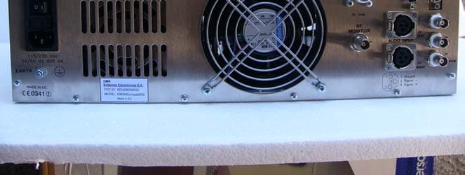
Click to zoom
Application Details
- Equipment Class
- TBC - Licensed Broadcast Station Transmitter
- Date of Grant
- Dec 20, 2006
- Application Purpose
- Original Equipment
- Date of Application
- Oct 19, 2006
- Equipment Note
- 250 Watt FM Broadcast Transmitter
- Frequency Range
- 88.00000000 - 108.00000000
- Country
- United States
Documents & Files
Document Text
Text extracted from the exhibit documents filed with the FCC. Open a document above to read the original.
Users Manual
TECHNICAL MANUAL v1.1 February 2006 SISTEMAS ELECTRONICOS S.A. 2 2 5 5 0 0 W W S S O O L L I I D D S S T T A A T T E E F F M M T T R R A A N N S S M M I I T T T T E E R R E E M M 2 2 5 5 0 0 C C O O M M P P A A C C T T D D I I G G OMB EUROPE: Factory: Camino de los Albares,14 -Ph. 976.50.35.80, Fax: 976.50.38.55 – 50410 CUARTE DE HUERVA (Zaragoza) ESPAÑA Sales Dpt.: Avda. San Antonio,41– Ph. 976.50.46.96, Fax: 976.46.31.70 – 50410 CUARTE DE HUERVA (Zaragoza) ESPAÑA E-mail:[email protected] Web:www.omb.es OMB USA: 3100 NW 72nd. Avenue Unit 112 – MIAMI, Florida 33122 – Ph.: 305 477-0973, 305 477-0974, Fax: 305 477-0611 E-mail:[email protected] Web:www.omb.com OMB ESPAÑA Av. San Antonio, 41 50410 Cuarte de Huerva ZARAGOZA (ESPAÑA) Website: http://www.omb.com e-mail: [email protected] Tlf: + 34 976 50 46 96 Fax: + 34 976 46 31 70 SISTEMAS ELECTRÓNICO S Nº Es01-022 Nº Es01-E021 LIMITED WARRANTY About Installation_____________________________________________________________ 1. - Mains Voltage must be kept between ±10% about its nominal value, unless otherwise specified. If were variations exceeding this tolerance, it will be indispensable to install a voltage stabilizer system within station. If transient overvoltages, due to electric motors, or other devices of this sort connected to the distribution line, were present, or if the distribution line is exposed to atmospheric electrical discharges, it must be indispensable the installation of isolation transformers and gaseous dischargers before connecting any equipment within station. 2. - All equipments must be connected to station ground system in order to avoid damage both to equipments and maintenance personnel too. It is necessary to connect a differential automatic switch (lifesaver) at station. 3. - Some equipments does not include interlock protection for open doors, covers or connectors. In that case, these equipments must be kept in key –locked places, with access only to conveniently qualified personnel that is previously noticed about not to open doors, covers or connectors without disconnecting station mains switch before performing this job. 4. - Transmitter equipments NEVER will be operated with output powers over its nominal values, or with signals or input informations others than those specified in its individual characteristics. 5. - Ambient temperature inside equipments' room, will accomplish technical specifications of equipments installed at station lodge. In absence of such specifications, maximum allowable temperatures will be from -5 to + 45ºC for Television equipments, and from 0 to + 40ºC for Sound Broadcast equipments. 6. - In case of operation at abnormally high or extremely high temperatures (over 30 to 40 º C), it is obligatory to install a forced cooling system that will keep temperature below its upper limit. In case of operation at abnormally or extremely low temperatures, it will be obligatory to install a thermostatic controlled heating system for equipment's room. 7. - Both equipment's surroundings and room must be free of dust and dirt. Ambient relative humidity will be kept below equipment's extreme specifications. In case of absence of this specification, allowable maximum will be 90 % of relative humidity, non-condensing. Average relative humidity will be kept under 70%, non-condensing. 8. - Every transmission equipment that can radiate some quantity of RF power, must be connected to a load or antenna system, suited to its individual specifications , before being energized. 9. - Maximum allowable VSWR in antenna systems both for Television or FM Radio Broadcast operation of a given transmitter, will be 1.25:1, unless otherwise specified. 10.- For those transmitter equipments having power valve amplifiers, and that doesn't has an automatic shutoff cycle, and must be manually turned off, as a first step high voltage, or anode voltage, will be disconnected, keeping forced cooling system working during at least 5 minutes after high voltage disconnection, and only after this time, cooling system & filament voltage can be shutted off. O.M.B. Sistemas Electrónicos, S.A., is not responsible of damages to those power valves caused by sudden AC mains failures at station where our equipments are installed. 11.- Periodically, monthly as a maximum, technical personnel must visit station in order to perform a general equipment maintenance, unless otherwise specified. This maintenance will include output power check, VSWR of antenna systems, forced cooling or heating systems checks, both for equipments and station itself, including air filters cleaning, measuring of transmission frequency with eventual correction if necessary, and will perform a general check of fundamental parameters of equipments. In the event of any important change in some operation parameter, that will require replacement or readjustment of any unit, Customer MUST CONTACT FIRST WITH O.M.B. SISTEMAS ELECTRONICOS, S.A. BEFORE ANY ATTEMPT TO READJUST OR REPLACE ANY COMPONENT OR UNIT INSIDE EQUIPMENTS, IN ORDER TO KEEP VALID THIS WARRANTY. 12.- For equipments who are located in fixed racks or cabinets, those equipments must be effectively connected, according to International Installations Standards, to station ground system, whose total impedance measured to ground can't be higher than 5 ohms. Equipments must be connected to ground system so that they can be kept out of main discharge path between tower and ground. About Transportation ___________________________________________________________ 1. - O.M.B. Sistemas Electrónicos, S.A. is not responsible of damages and/or detriments derived from mishandling, steal, robbery, theft or vandalism during the act of transportation of equipments to final or intermediate destination. About Storage ________________________________________________________________ 1. - O.M.B. Sistemas Electrónicos, S.A. is not responsible of damages and/or detriments derived from unappropiate storage of equipments, within inadequate warehous…
Text truncated - open the document above for the full version.
Users Manual
06/06/02 OMB Eng. Dpt. Driver FM v1.2 7W FM Driver 05.01.01.000 1234 A B C D 4 321 D C B A Drawn Checked Standards DateNameSignature: Scale:TitleDrawing nr: Replace: Replaced with: Sistemas Electrónicos S.A. FM Transmitter Sistemas Electrónicos S.A EM 250 COMPACT DIG Technical Manual - v1.1 - February 2006 37 FM 300W Power Amplifier DESCRIPTIONREFERENCEQUANTITY Cap. 33pF SMD 1206 100V C1 1 Cap. 470pF SMD 1210 5% 200V NPO C2, C11-C14 5 Cap. 1nF SMD 1206 100V C3-C6, C16,C20 6 Cap. 150pF 100V Ceramic C7,C8 2 Cap. 100uF SMD t50V Electrolytic C15 1 Cap. 22nF SMD 1206 200V Ceramic X7R C17 1 Cap. 47pF SMD 1210 5% 500V C17 C18 1 Cap. 15pF SMD 1210 5% 500V C17 C19 1 Diode BAT54 SMD SOT-23 D1,D2 2 Zener diode 10V SMD 0.35W D4 1 Thread0.8mm Cu-Ag 30mm. approx. Material for L1 and TR2 fixing Thread1mm Cu enamelled 250mm. approx. Material for L2 Thread1.5mm Cu-Ag 50mm. approx. Material for L5 and TR1 fixing Axial ferrite L3,l4 2 Output transformer core L5 1 22: SMD 1206 1/4W r2,r3 2 Potentiometer 1turn 1K 3/8” R4 1 Metal 1 : / 2W L=12mm =3.9mm Non-inductive R5 1 Res. 10: SMD 1206 1/4W R6-R9 4 Res. 10: Coal 2W L=16mm =5.5mm Non-inductive R10 1 Res. 330: SMD 1206 R11 1 Res. 110: SMD 1206 R12 1 Res. 1K8: SMD 1206 R14 1 Res. 10: SMD 0805 R15 1 Output Transformer TR1 1 Input Transformer TR2 1 Connection terminals tab 2.8x0.5 CON1,CON2 2 Female-female hex. separator 10mm Brass-Nickel CON3 1 MOSFET, N 108MHz 300W SALD BLF278 Q1 1 04/05/04 M. Tsvelev MODPOT v1.3 04.04.01.003 300W R.F. Power Amplifier 1 2 3 4 5 6 78 ABCD 8 7 6 5 4 3 2 1 D CBA Drawn Checked Standards Date Name Signature: Scale :T i t le: Drawing nr: Replace : Replaced with : Sistemas Electrónicos S.A. R1300* C133pF TR2 Input Transf. C2470pF C51nF C7150pF C912pF* C11470pF C1847pFC1915pF C31nF R51R 2W R651R7RF 100 Ohm R222 R322 R11330 GND GND D2BAT54 R4P1K GND C41nF GND +12V Polarization L1Bridge GND GND GND C61nF C8150pF R951R8RF 100 Ohm GND C1012pF* GND TR2 Output Transf. GNDGND GNDGND L2 Dext8 8 turns Dcable 0.8-1 R1010 Ohm 2W C15 100uF C16 1nFC1722nF GNDGNDGND +48v GND C12470pF C13470pF C14470pF GND D1BAT54 R12110 BIAS Off C201nF R1310K* D3LED* GND RF In RF Out Elements with * are optional Q1 BLF278 L3Ferrit e L4Ferrit e L5 Core D4BZX84C10 R141K8 GND R1510 Date Drawn Checked Name Standards Signature: Scale: Title: Drawing nr: Replace: Replaced with: Sistemas Electrónicos S.A. 04/05/04 M. Tsvelev MODPOT v1.3 300W R.F. Power Amplifier 06/06/02 OMB Eng. Dpt. EM 250 COMPACT DIG 05.04.02.000 300W FM FIlter 1 2 3 4 5 6 78 ABCD 8 7 6 5 4 3 2 1 D CBA Drawn Checked Standards Date Name Signature: Scale :T i t le: Drawing nr: Replace : Replaced with : Sistemas Electrónicos S.A. RF IN L3 3V D9mm d1.5mm L2 3V D9mm d1.5mm L14V D9mm d1.5mm TL150 Ohm TL4 Forward Power TL2 Monitor TL3 Reflected Power RF OutOutput Coupling Monitor R11120R R351R R5 1K R710K R9120R R251RR151R R451R R61K R810K R10120R C81nF C91nF C101nF C111nF C722pF C522pF C622pF D2BAT54 D1BAT54 C251pF500V RF C125pF500V RF C351pF500V RF C425pF500V RF C124.7pF500V RF C14 12pF 500V RF C13 9.1pF 500V RF Reflected Coupling In case of using AD250 substrate C15 = 6.8pF ; C14 = 2x 5.6pF R9 = R10 = R11 = 150 ohms FM Transmitter Sistemas Electrónicos S.A EM 250 COMPACT DIG Technical Manual - v1.1 - February 2006 41 2.6 Control unit and display board. This circuit board is basically simple.It contains the Microcontroller,the keyboard and few other circuits which we will briefly discuss.Control and Display Units are shown in Figure 2-7 below. The Microcontroller has 3 digital 8-bit ports and an analog one. This latter is the interface with the analog signals that must be measured in the transmitter. A fast peak rectifier built around IC4 drives one of these analog lines. All audio or baseband modulation plus some steady state signals are multiplexed to its input by IC3, so requiring only one peak rectifier and increasing the number of the analog channels. One analog channel reads the internal temperature through the optional TR3 sensor. Fig. 2-7: DETAILED VIEW OF CONTROL UNIT. The simple specialized IC6 performs clock and date functions as a stand-alone unit, backed-up by a NiMnh battery which keeps circuit active for a long time when the power is removed. Fig. 2-8: DETAILED VIEW OF DISPLAY and EXTERNAL CONTROL BOARD. Elements numbered in Figure 2-8 are the following: 1 - MAIN/STANDBY push button switch. 2 - STANDBY indicator LED. 3 - ALARM indicator LED. 4 - VSWR indicator LED. 5 - LIMITER indicator LED. FM Transmitter Sistemas Electrónicos S.A EM 250 COMPACT DIG Technical Manual - v1.1 - February 2006 42 6 - DISPLAY CONTRAST adjustment potentiometer. 7 - REMOTE operation indicator LED. 8 - LOCK indicator LED. 9 - ON THE AIR indicator LED. 10 - External control keyboard. 11 - CANCEL key, to suppress any order or command. 12 - OK data entering key, to confirm any order or command. 13 - Two-row, backlighted alphanumeric LCD display. The keyboard switch set is sequentially interrogated one hundred times in a second to determine if a key was pushed. IC5,a serial to parallel converter, drives the front-panel LEDs and the display backlighting with TR2. The alphanumeric display is a separate module, connected to the board by a small flat-ribbon cable, as shown in Figure 2-8. 11 digital lines from the Microcontroller drive this module. The internal board potentiometer RT1 regulates the LCD contrast and may be used to change it for different situations. A separate power supply current for the backlight LEDs is provided by R41 and R42: these resistors become quite hot when the display is full on and their heat someway influence the internal temperature read by TR3. No other regulation is provided on the board.The precision of the measurements is guaranteed by design by the precision of the components and the reference voltage source IC1. 18/04/03 OMB Eng. Dpt. EM 250 COMPACT DIG Control unit 1 2 3 4 5 6 78 ABCD 8 7 6 5 4 3 2 1 D CBA Drawn Checked Standards Date Name Signature: Scale :T i t le: Drawing nr: Rep…
Text truncated - open the document above for the full version.
External Photos
EXTERNAL CONSTRUCTION PHOTOS OF EM250DIG Top View Bottom View Front View Rear View (FCC label is on left hand side)
Internal Photos
INTERNAL CONSTRUCTION PHOTOS OF EM250DIG Top Without Main Cover Top without main cover and RF Amp cover Top From Right without Main Cover Top from left without main cover Behind Front Panel
Operational Description
1.2 Description. The EM-250 COMPACT DIG is a 250W rated, direct-synthesis, FM-modulated transmitter. Being digitally controlled, it is extensively put on the air on field by front panel or remotely in additional aspects: frequency, power, channel sensitivity, pre-emphasis, functioning mode (mono, stereo, external mpx), clock and date and many other parameters without adjusting or substituting any part. A powerful 3-level password management permits a very high degree of security and privacy as may be required in different situations. Equipment requires little or no maintenance and its simple modular layout facilitates stage testing and servicing. As imposed by various national standards, these transmitters incorporate sophisticated low-pass audio filters on mono and stereo channels, and a sharp acting modulation limiter, which is usually set at a peak deviation slightly higher than 75kHz. Its intervention may nevertheless be avoided, if required, presetting its threshold at a deviation higher than 150kHz. Output frequency is phase- locked to a temperature-compensated crystal oscillator, which ensures superior precision and stability. A very low noise, low distortion VCO produces a harmonic-free, spurious-free signal. A lock control circuit inhibits the presence of power on the output until the apparatus is on the right frequency, when turning on. To lower the noise threshold further, the low-frequency inputs are fitted with balanced input circuitry. The input level is precisely adjustable over a broad range, by means of a 0.5dB stepwise variable attenuators. The transmitter has an auxiliary input, specifically designed for RDS and SCA encoders. A modulation sample output permits to control other transmitters or STL's with the same internally processed high-quality mpx signal. The alphanumeric display permits easy and accurate metering, adjustment and continuous monitoring of modulation levels, power, operation and internal parameters. All these information may be externally available on the same RS-232 I/O bus that may be used to remotely control the transmitter. Above Figure 1-1 shows us the external view of Modulator / Exciter's cabinet, whose control panel has been simplified to a maximum, being Microcontroller in charge of practically to select and make all tests and adjustments of all parameters that are relevant to the normal Equipment's performance. Due to this fact, Front Panel has only a few control elements, since with only the four push buttons pertaining to Microcontroller (like those used to control movement of cursor in a Computer) and two keys, these virtually controlling all processes and parameters having place within Equipment. Microcontroller uses a Liquid-Crystal dot matrix as Alphanumeric Display unit in order to watch parameter's values, as it's asked for it, as can be seen in the corresponding section in this Manual. In addition to the serial I/O port, some signals (RF power, ON THE AIR status, Disable line) are available on a parallel I/O remote socket for easy interfacing with others analog controllers or supervisory systems. A top-quality stereo encoder may be factory installed as option and even retrofitted in the field in a second time, requiring minimum technical skill. The powerful internal software and monitoring functions recognizes its presence and enables its functions. The RF power amplifier employs a broadband design and has a lot of reserve: the output power is feedback-controlled for increased stability still higher than nominal level. High reflected power is limited to prevent output stage degradation; direct power is accordingly continuously reduced so as not to exceed the reflected power safety level. A sturdy telecom-grade high efficiency switch-mode power supply allows operation in a very wide and noisy mains environment.
Parts List/Tune Up Info
FM EXCITER BOARD COMPONENTDESCRIPTION FORMAT C1100uF 16VSMD C2100n1206 SMD C31N1206 SMD C41N1206 SMD C41N1206 SMD C533P1206 SMD C682P1206 SMD C7100P1206 SMD C7100P1206 SMD C8100P1206 SMD C9100N1206 SMD C10100N1206 SMD C11470N1206 SMD C12100N1206 SMD C131N1206 SMD C151N1206 SMD C16100N1206 SMD C17100U 16VSMD C18100N1206 SMD C19470N1206 SMD C2010U 16V2512 SMD C21100N1206 SMD C221N1206 SMD C231N1206 SMD C24330P1206 SMD C2510P1206 SMD C251N1206 SMD C261N1206 SMD C271N1206 SMD C281N1206 SMD C301N1206 SMD C32100N1206 SMD C33100N1206 SMD C34100N1206 SMD C351N1206 SMD C36220P1206 SMD C371N1206 SMD C3833P1206 SMD C39220P1206 SMD C4068P1206 SMD C411U1206 SMD C42100P1206 SMD C431N1206 SMD C441N1206 SMD C45100P1206 SMD C4627P1206 SMD C4727P1206 SMD C483P31206 SMD C49100P1206 SMD C51100N1206 SMD C52100U 16VSMD C53100N1206 SMD C54100N1206 SMD C55100N1206 SMD 09/08/061/3 C56100N1206 SMD D1BAT54SSOT23 SMD D2BAT54SSOT23 SMD D3BAT54SSOT23 SMD D4BB153SOT23 SMD D5BB153SOT23 SMD D6BB153SOT23 SMD D7BB153SOT23 SMD D8BAW56SOT23 SMD DZ1C9V1SMD IC1LM358SOIC8 SMD IC2MB1501SOIC16 SMD L1100uH2512 SMD L101U2512 SMD L11100N2512 SMD L12220N2512 SMD L5470N2512 SMD L62U22512 SMD L81U2512 SMD L9220N2512 SMD R01470R1206 SMD R0210K1206 SMD R03330R1206 SMD R04330R1206 SMD R05100R1206 SMD R061M1206 SMD R071M1206 SMD R08100K1206 SMD R092M21206 SMD R101M1206 SMD R11150K1206 SMD R12220K1206 SMD R1347K1206 SMD R14100K1206 SMD R15100K1206 SMD R16220R1206 SMD R17220R1206 SMD R18100R1206 SMD R1910K1206 SMD R2015K1206 SMD R21330R1206 SMD R220R01206 SMD R230R01206 SMD R240R01206 SMD R25330R1206 SMD R2647R1206 SMD R27100R1206 SMD R28100R1206 SMD R2910K1206 SMD R30330R1206 SMD R3122R1206 SMD R32220R1206 SMD R3327K1206 SMD R34180R1206 SMD R3547R1206 SMD R3647R1206 SMD 09/08/062/3 R3747R1206 SMD R38100R1206 SMD R39100R1206 SMD R4056R1206 SMD R411K1206 SMD R4210R1206 SMD R441K1206 SMD R4556R1206 SMD R461R1206 SMD R48220K1206 SMD R492K21206 SMD R5010K1206 SMD R5110K1206 SMD R521K51206 SMD R5310K1206 SMD R54470R1206 SMD R55470R1206 SMD R56100R1206 SMD R571K1206 SMD R581K1206 SMD R591K51206 SMD R603K31206 SMD R614K71206 SMD R624K71206 SMD R634K71206 SMD R64100K1206 SMD R65100K1206 SMD RT110KSMD TR1BCR133SOT23 SMD TR2BCR133SOT23 SMD TR3BCR133SOT23 SMD TR4BFR93ASOT23 SMD TR5SST310SOT23 SMD TR6SST310SOT23 SMD TR7BFR93ASOT23 SMD TR8BFR93ASOT23 SMD TR9BSP122SOT223 SMD TR10BSP122SOT223 SMD TXCO112.6MHZSMD 09/08/063/3 MAINBOARD COMPONENTDESCRIPTION FORMAT C1100U 25VSMD C2100U 25VSMD C31N1206 SMD C41N1206 SMD C51N1206 SMD C61N1206 SMD C71N1206 SMD C8220P1206 SMD C910P1206 SMD C1010P1206 SMD C1110P1206 SMD C1210P1206 SMD C13100N1206 SMD C1322P1206 SMD C14100N1206 SMD C15100N1206 SMD C16100N1206 SMD C17100N1206 SMD C18100N1206 SMD C211N1206 SMD C221N1206 SMD C231N1206 SMD C231N1206 SMD C24100P1206 SMD C24100P1206 SMD C24100P1206 SMD C241N1206 SMD C25100P1206 SMD C251N1206 SMD C26100P1206 SMD C261N1206 SMD C271N1206 SMD C29100N1206 SMD C30100N1206 SMD C301N1206 SMD C31100N1206 SMD C32100N1206 SMD C334N71206 SMD C3322N1206 SMD C341N1206 SMD C36470P1206 SMD C3622N1206 SMD C3747K1206 SMD C391N1206 SMD C41100N1206 SMD C471U1206 SMD C481U1206 SMD C49100N1206 SMD C50100N1206 SMD C51100N1206 SMD C54100N1206 SMD C55100N1206 SMD C56100P1206 SMD 09/08/061/6 C572N21206 SMD C582N21206 SMD C5947P1206 SMD C6047P1206 SMD C611N1206 SMD C621N1206 SMD C63220P1206 SMD C6447P1206 SMD C64220P1206 SMD C652N21206 SMD C662N21206 SMD C6847P1206 SMD C6910N1206 SMD C7010N1206 SMD C714N71206 SMD C7210N1206 SMD C738N21206 SMD C7410N1206 SMD C758N21206 SMD C7610N1206 SMD C77100N1206 SMD C78100N1206 SMD C79100N1206 SMD C80100N1206 SMD C81100N1206 SMD C82100N1206 SMD C8347N1206 SMD C841N1206 SMD D1BAV99SOT23 SMD D10BAV99SOT23 SMD D11BAW56SOT23 SMD D12BAW56SOT23 SMD D13BAW56SOT23 SMD D14BAW56SOT23 SMD D15BAV99SOT23 SMD D16BAV99SOT23 SMD D17BAV99SOT23 SMD D18BAV99SOT23 SMD D2BAV99SOT23 SMD D3BAV99SOT23 SMD D4BAV99SOT23 SMD D5BAV99SOT23 SMD D6C12V0ZENER DIODE SMD D7C12V0ZENER DIODE SMD D8C5V6ZENER DIODE SMD D9BAV99SOT23 SMD DZ1C12V0ZENER DIODE SMD DZ2C12V0ZENER DIODE SMD DZ3C5V1ZENER DIODE SMD DZ4C6V2ZENER DIODE SMD DZ5C6V2ZENER DIODE SMD IC1TL074SOIC14 SMD IC2TL074SOIC14 SMD IC3MC34082SOIC14 SMD IC4TL074SOIC14 SMD 09/08/062/6 IC575155 SOIC14 SMD IC7TL072SOIC14 SMD IC8TL1973WSOIC20 SMD IC8TL072SOIC14 SMD IC94316 SOIC14 SMD IC10TL074SOIC14 SMD IC11TL074SOIC14 SMD IC12TL074SOIC14 SMD IC13MC34084SOIC14 SMD IC144052BSOIC16 SMD IC154094BSOIC16 SMD J5RS232 DB9F JP1JUMPER3 JP2JUMPER3 L11U2512 SMD L21U2512 SMD P1IDC26 P6IDC10 P9IDC14 R015K61206 SMD R025K61206 SMD R035K61206 SMD R045K61206 SMD R0510K1206 SMD R0682R1206 SMD R0782R1206 SMD R08560R1206 SMD R09560R1206 SMD R10100R1206 SMD R11100R1206 SMD R12100R1206 SMD R13100R1206 SMD R14100R1206 SMD R1510K1206 SMD R15100R1206 SMD R1610K1206 SMD R1710K1206 SMD R1810K1206 SMD R195K61206 SMD R195K61206 SMD R205K61206 SMD R205K61206 SMD R244K71206 SMD R254K71206 SMD R26220R1206 SMD R2610K1206 SMD R2710K1206 SMD R2810K1206 SMD R33470R1206 SMD R3410K1206 SMD R354K71206 SMD R3656K1206 SMD R3756K1206 SMD R38270R1206 SMD R39270R1206 SMD 09/08/063/6 R4010K1206 SMD R4110K1206 SMD R421K1206 SMD R431K1206 SMD R443K91206 SMD R453K91206 SMD R461K1206 SMD R461K1206 SMD R471K1206 SMD R481K1206 SMD R49100K1206 SMD R49100K1206 SMD R50100K1206 SMD R51100R1206 SMD R5256K1206 SMD R5315K1206 SMD R543M31206 SMD R561K51206 SMD R57470R1206 SMD R58475R1206 SMD R59475R1206 SMD R596K81206 SMD R60475R1206 SMD R6015K1206 SMD R6115K1206 SMD R6215K1206 SMD R6315K1206 SMD R6410K1206 SMD R70820R1206 SMD R71820R1206 SMD R722K21206 SMD R731K81206 SMD R741K81206 SMD R7533R1206 SMD R7633R1206 SMD R77470R1206 SMD R78470R1206 SMD R7910K1206 SMD R8010K1206 SMD R83180R1206 SMD R84180R1206 SMD R85680R1206 SMD R86680R1206 SMD R8722K1206 SMD R8822K1206 SMD R891M1206 SMD R901M1206 SMD R911K81206 SMD R921K81206 SMD R93470R1206 SMD R941K81206 SMD R953K31206 SMD R96470R1206 SMD R97100K1206 SMD R985K61206 SMD 09/08/064/6 R99220R1206 SMD R100180R1206 SMD R101560R1206 SMD R102560R1206 SMD R1036K81206…
Text truncated - open the document above for the full version.
Schematics
Date Drawn Checked Name Standards Signature: Scale: Ttle: Drawing nr: Replace: Replaced with: Sistemas Electrónicos S.A. OMB Eng. Dpt. EM 250 COMPACT DIG General cabinet layout Date Drawn Checked Name Standards Signature: Scale: Ttle: Drawing nr:: Replace: Replaced with: Sistemas Electrónicos S.A. OMB Eng. Dpt. EM 250 COMPACT DIG Inner layout OMB Eng. Dpt. EM 250 COMPACT DIG General wiring diagram 1 2 3 4 5 6 78 ABCD 8 7 6 5 4 3 2 1 D CBA Drawn Checked Standards Date Name Signature: Scale :T i t le: Drawing nr: Replace : Replaced with : Sistemas Electrónicos S.A. 01/11/04 OMB Eng. Dpt. EM 250 COMPACT DIG MAINBOARD - I/O & R.F. Control Section 1 2 3 4 5 6 78 ABCD 8 7 6 5 4 3 2 1 D CBA Drawn Checked Standards Date Name Signature: Scale :T i t le: Drawing nr: Replace : Replaced with : Sistemas Electrónicos S.A. 101/11/04 OMB Eng. Dpt. EM 250 COMPACT DIG MAINBOARD - LF Process Section 1 2 3 4 5 6 78 ABCD 8 7 6 5 4 3 2 1 D CBA Drawn Checked Standards Date Name Signature: Scale :T i t le: Drawing nr: Replace : Replaced with : Sistemas Electrónicos S.A. Date Drawn Checked Name Standards Signature: Scale: Title: Drawing nr: Replace: Replaced with: Sistemas Electrónicos S.A. 01/11/04 OMB Eng. Dpt. EM 250 COMPACT DIG Mainboard 01/11/04 OMB Eng. Dpt. EM 250 COMPACT DIG Stereo encoder 1 2 3 4 5 6 78 ABCD 8 7 6 5 4 3 2 1 D CBA Drawn Checked Standards Date Name Signature: Scale :T i t le: Drawing nr: Replace : Replaced with : Sistemas Electrónicos S.A. Date Drawn Checked Name Standards Signature: Scale: Title: Drawing nr: Replace: Replaced with: Sistemas Electrónicos S.A. 01/11/04 OMB Eng. Dpt. EM 250 COMPACT DIG Stereo encoder 01/11/04 OMB Eng. Dpt. EM 250 COMPACT DIG FM Exciter 1 2 3 4 5 6 78 ABCD 8 7 6 5 4 3 2 1 D CBA Drawn Checked Standards Date Name Signature: Scale :T i t le: Drawing nr: Replace : Replaced with : Sistemas Electrónicos S.A. Date Drawn Checked Name Standards Signature: Scale: Title: Drawing nr: Replace: Replaced with: Sistemas Electrónicos S.A. 01/11/04 OMB Eng. Dpt. EM 250 COMPACT DIG FM Exciter 06/06/02 OMB Eng. Dpt. EM 250 COMPACT DIG 05.04.01.001 7W FM Driver 1 2 3 4 5 6 78 ABCD 8 7 6 5 4 3 2 1 D CBA Drawn Checked Standards Date Name Signature: Scale :T i t le: Drawing nr: Replace : Replaced with : Sistemas Electrónicos S.A. R1 1R 2W R3 1K8 0.5W D21N5363B-30V o 28V C1100nF C210uF GND GND GND 28V Q2TIP3055 R2 1R 2W Q1 BLF242 C668pF C3150pF C7 1nF C9 10nF C81nF C4 220pF C518pF C1010nF R422R R8220 R9220 R1251 R131K R101K R1410R 0.5W R111KL150nH L2 50nH L4 VK200 RF IN RF OUT L3VK200 28V R722R 1W R5220 1W R6220 1W TL1 33 OHM TL2 33 OHM +48V D41N4148D3BZX55C5V1 BIAS R15680R 06/06/02 OMB Eng. Dpt. Driver FM v1.2 7W FM Driver 05.01.01.000 1234 A B C D 4 321 D C B A Drawn Checked Standards DateNameSignature: Scale:TitleDrawing nr: Replace: Replaced with: Sistemas Electrónicos S.A. 04/05/04 M. Tsvelev MODPOT v1.3 04.04.01.003 300W R.F. Power Amplifier 1 2 3 4 5 6 78 ABCD 8 7 6 5 4 3 2 1 D CBA Drawn Checked Standards Date Name Signature: Scale :T i t le: Drawing nr: Replace : Replaced with : Sistemas Electrónicos S.A. R1300* C133pF TR2 Input Transf. C2470pF C51nF C7150pF C912pF* C11470pF C1847pFC1915pF C31nF R51R 2W R651R7RF 100 Ohm R222 R322 R11330 GND GND D2BAT54 R4P1K GND C41nF GND +12V Polarization L1Bridge GND GND GND C61nF C8150pF R951R8RF 100 Ohm GND C1012pF* GND TR2 Output Transf. GNDGND GNDGND L2 Dext8 8 turns Dcable 0.8-1 R1010 Ohm 2W C15 100uF C16 1nFC1722nF GNDGNDGND +48v GND C12470pF C13470pF C14470pF GND D1BAT54 R12110 BIAS Off C201nF R1310K* D3LED* GND RF In RF Out Elements with * are optional Q1 BLF278 L3Ferrit e L4Ferrit e L5 Core D4BZX84C10 R141K8 GND R1510 Date Drawn Checked Name Standards Signature: Scale: Title: Drawing nr: Replace: Replaced with: Sistemas Electrónicos S.A. 04/05/04 M. Tsvelev MODPOT v1.3 300W R.F. Power Amplifier 06/06/02 OMB Eng. Dpt. EM 250 COMPACT DIG 05.04.02.000 300W FM FIlter 1 2 3 4 5 6 78 ABCD 8 7 6 5 4 3 2 1 D CBA Drawn Checked Standards Date Name Signature: Scale :T i t le: Drawing nr: Replace : Replaced with : Sistemas Electrónicos S.A. RF IN L3 3V D9mm d1.5mm L2 3V D9mm d1.5mm L14V D9mm d1.5mm TL150 Ohm TL4 Forward Power TL2 Monitor TL3 Reflected Power RF OutOutput Coupling Monitor R11120R R351R R5 1K R710K R9120R R251RR151R R451R R61K R810K R10120R C81nF C91nF C101nF C111nF C722pF C522pF C622pF D2BAT54 D1BAT54 C251pF500V RF C125pF500V RF C351pF500V RF C425pF500V RF C124.7pF500V RF C14 12pF 500V RF C13 9.1pF 500V RF Reflected Coupling In case of using AD250 substrate C15 = 6.8pF ; C14 = 2x 5.6pF R9 = R10 = R11 = 150 ohms 18/04/03 OMB Eng. Dpt. EM 250 COMPACT DIG Control unit 1 2 3 4 5 6 78 ABCD 8 7 6 5 4 3 2 1 D CBA Drawn Checked Standards Date Name Signature: Scale :T i t le: Drawing nr: Replace : Replaced with : Sistemas Electrónicos S.A. Date Drawn Checked Name Standards Signature: Scale: Title: Drawing nr: Replace: Replaced with: Sistemas Electrónicos S.A. 18/04/03 OMB Eng. Dpt. EM 250 COMPACT DIG Control unit Component sideSolder side 16/07/02 OMB Eng. Dpt. EM 250 COMPACT DIG Keyboard/display interface 1 2 3 4 5 6 78 ABCD 8 7 6 5 4 3 2 1 D CBA Drawn Checked Standards Date Name Signature: Scale :T i t le: Drawing nr: Replace : Replaced with : Sistemas Electrónicos S.A. Date Drawn Checked Name Standards Signature: Scale: Title: Drawing nr: Replace: Replaced with: Sistemas Electrónicos S.A. 16/07/02 OMB Eng. Dpt. EM 250 COMPACT DIG Keyboard / display interface COMPONENT SIDE SOLDER SIDE 18/07/00 EM 250 COMPACT DIG Switching Power Supply SP-500/48A 1 2 3 4 5 6 78 ABCD 8 7 6 5 4 3 2 1 D CBA Drawn Checked Standards Date Name Signature: Scale :T i t le: Drawing nr: Replace : Replaced with : Sistemas Electrónicos S.A. SP-500A DIFFERENT COMPONENT:PART NO. MODEL R31 ZD4 2.2u/50V C25 CN2 V- 2.2u/50V C24 HER104 D7 TR134 L1 HER104 D8 NC(PSF) P5 Terminal R+ 30K/2W R18 220u/25V C17 104/100V C21 C1815 Q7 470u/25V C23 1K R24 2K2 R23 1N4001 D2 R31 A562 Q8 ZD4 CN4 X X X 8.9V 8.9V 8.9V 13.5V 12V 15V 2K2 R25 2.2u/50V C22 24V 27V 48V X X 8.9V 8.9V 8.9V C…
Text truncated - open the document above for the full version.
Test Report
1/51 SISTEMAS ELECTRONICOS, S.A FABRICA: Camino de los Albares, 14 Tlf. 976.50.35.80 (6 líneas). Fax: 976.50.38.55 50410 CUARTE DE HUERVA (Zaragoza ) DOCUMENTO TÉCNICO INGENIERÍA / TECHNICAL DOCUMENTATION PARA/TO:DE/FROM: OMB ORGANIZACIÓN/ORGANIZATION:FECHA/DATE: June 16 2006 NÚMERO DE FAX/FAX NUMBER:Nº DE REFERENCIA DEL REMITENTE/OUR REF. NUMBER: IT-04050603 ASUNTO/SUBJECT:SU Nº DE REFERENCIA/YOUR REF. NUMBER: EM250CompactDig Measurements Measurements for type certification of FM transmitters. • All the measurements done are valid for the unit tested identified with the serial number noted in the identification section, this unit was randomly selected. The results are valid also for the general and particular conditions specified. • All the measurements are done in the OMB laboratory except the measurements for cabinet radiation, which was done in the external laboratory of Ministerio de industria, turismo y comercio de España; Dirección general de telecomunicaciones y tecnologías de la información; Radiofrequency Laboratory • I DENTIFICATION . Class:FM transmitter Model:EM250CompactDIG Nominal power:250W (Adjustable from 0 to 250W) Manufacturer:OMB Sistemas Electrónicos, S.A. Country of manufacturing:Spain Address:Avda. San Antonio 41, 50410 Cuarte de Huerva, Zaragoza, Spain. E QUIPMENT U NDER T EST (EUT)= EM250C OMPACT DIG S ERIAL NUMBER 60158 2/51 • L IST OF TEST INSTRUMENTS USED FOR THE MEASUREMENTS DONE IN THE OMB LABORATORY ( EXCLUDES CABINET RADIATION TEST ): EquipmentManufacturerModelSerial Number WattmeterBird43912442 Spectrum AnalyzerAdvantestR3131J003753 Modulation AnalyzerHP8901B3226A04087 Audio AnalyzerHP8903B2910A06154 Dynamic Signal AnalyzerHP3562A2502A01080 RF CouplerBirdCU-2340/SRCA1240 Thermal ChamberACS (Angelantoni Centro-Sud) UY-3001940/B/7 Dummy LoadLSI (Lear Siegler Inc) 160B600X1499 MultimeterFluke27/FM662…
Text truncated - open the document above for the full version.
Contact Information
Applicant
Antonio Ormad Moya(President)
Technical Contact
Greg Best Consulting, Inc.Greg Best
[email protected]816-792-2913
9223 N. Manning Avenue · Kansas City, Missouri · United States
Technical Specifications
| # | Rule Parts | Frequency Range | Power Output | Emission | Tolerance |
|---|---|---|---|---|---|
| 1 | 73,74 | 88 MHz - 108 MHz | 250 W | 300KF8E | 1000.0000000000 Hz |
Other Applications from Transamerica International Broadcasting Inc
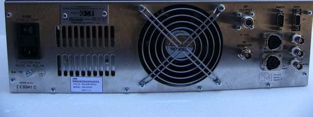
KEUEM100DIG
Dec 20, 2006100 Watt FM Broadcast Transmitter
Equipment Class
TBC - Licensed Broadcast Station Transmitter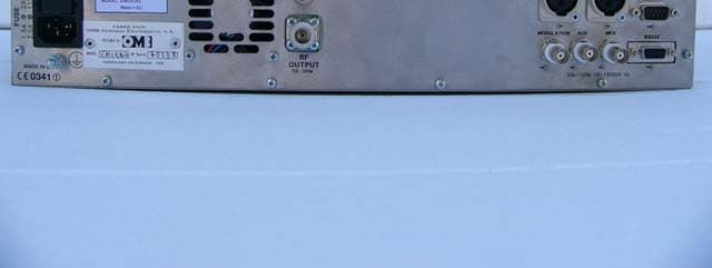
KEUEMDIG25
Dec 07, 200625 Watt FM Broadcast Transmitter
Equipment Class
TBC - Licensed Broadcast Station TransmitterKEUAMPAM20000
Aug 10, 1998TBC - Licensed Broadcast Station Transmitter
Equipment Class
TBC - Licensed Broadcast Station TransmitterKEUOMBSTLMT5
Apr 28, 1997Approved For Fixed Operation Only.
Equipment Class
TBC - Licensed Broadcast Station TransmitterKEUOMBEXCEM100
Apr 06, 1997TBC - Licensed Broadcast Station Transmitter
Equipment Class
TBC - Licensed Broadcast Station Transmitter