KVCKS-1717" TFT-LCD Monitor
Ksai Electronics Co Ltd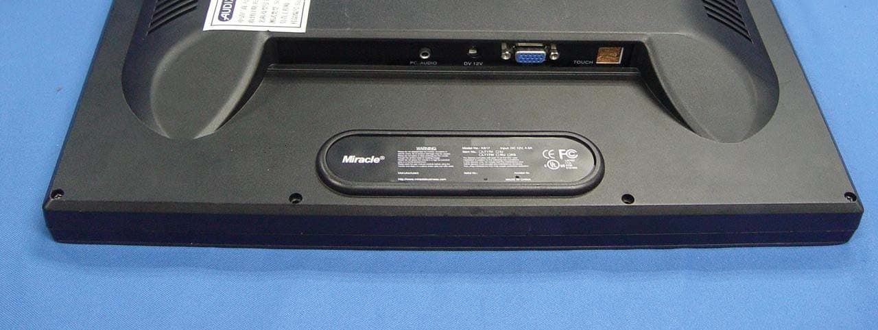
Click to zoom
Application Details
- Equipment Class
- JBP - Part 15 Class B Computing Device Peripheral
- Date of Grant
- Jul 05, 2007
- Application Purpose
- Original Equipment
- Date of Application
- Jul 05, 2007
- Equipment Note
- 17" TFT-LCD Monitor
- Company
- Ksai Electronics Co Ltd
- Country
- China
Documents & Files
Document Text
Text extracted from the exhibit documents filed with the FCC. Open a document above to read the original.
Users Manual
TFT-LCD Monitor 74-520007-000 TFT-LCD Monitor USER’S MANUAL INDEX Precautions............................................................... 2 Federal Communication Commission Radio Frequency International Statement ............................................... 3 Canadian Department Of Communications Compliance Statement.................................................................. 3 Product Description................................................... 4 Package Contents...................................................... 4 Product Features....................................................... 4 Cleaning.................................................................... 4 Taking a Look............................................................ 5 Front View................................................................. 5 Rear View................................................................. 6 Computer connecting................................................. 6 Controls and Adjustment............................................. 6 OSD Control Options.................................................. 7 Power LED Display & Power Saving............................. 11 Troubleshooting......................................................... 11 Specifications............................................................ 12 -1- Precautions Read all of these instructions and save them for later use. Follow all warnings and instructions on the product. Product - Do not cover or block the vent holes in the case. - Do not insert sharp objects or spill liquid into the LCD monitor through cabinet slots. They may cause accident fire, electric shock or failure. - Disconnect the power plug from the AC outlet if you will not use it foe an indefinite period of time. - Do not attempt to service this product yourself, as opening or removing covers may expose you to dangerous voltage points or other risks. - Do not touch the screen directly with your fingers. You may damage the screen, and oil from you skin is difficult to remove. - Do not apply pressure to the sc reen. The LCD is very delicate. Power adapter - Use the type of power adapter, which supplies fr om manufacturer for safety and electronic issue. Plugs - Do not remove any of the prongs of the monitor’s three-pronged power plug. - Disconnect the power plug from the AC outlet under following conditions: If you will not use it for an indefinite period time. When the power cord or plug is damaged or frayed. If the product does not operate normally when the operating instructions are followed. Adjust only those controls that are covered by the operating in structions. Improper adjust ment of other controls may result in damage and will often require extens ive work by a qualified technician to restore the product to normal operation. If the product has been dropped or the cabinet has been damaged. If the product exhibits a distinct change in performance, indicating a need for service. Power and extension cords - Do not allow anything to rest on the power cord. - Do not locate this product where persons will walk on the cord. - Use the proper power cord with correct attachment plug type. If the power source is 120 V AC, use a power cord that has UL and C-UL approvals. If the pow er source is a 240 V AC supply, use the tandem (T blade) type attachment plug with gr ound conductor power cord that meets the respective European country's safety regulations, such as VDE for Germany. - Do not overload wall outlets or power cords. Ensure th at the total of all units plugged into the wall outlet does not exceed 10 amperes. - Ensure that the total ampere ratings on all units plugg ed into the extension cord is not above the cord's rating. - If the power supply cord, which came with your monitor, is to be connected to the PC instead of the wall outlet, this equipment is to be used with UL a pproved computers with receptacle rated 240V AC, 4.0A (minimum). - The socket outlet shall be inst alled near the LCD monitor and shall be easily accessible. -2- Environment - Place the monitor on a flat and leveled surface. - Place the monitor in a well-ventilated place. - Keep the monitor away from: overly hot, cold or humid places, places directly under sunlight, dusty surroundings, equipment that ge nerate strong magnetic fields. Federal Communication Commission Radio Frequency International Statement This equipment has been tested and found to comply with the limits for a Class B dig ital device, pursuant to part 15 of the FCC Rules. These limits are designed to provide reasonable protection against harmful interference in a residential installation. This equipment generates, us es and can radiate radio frequency energy and, if not installed and used in accordance with the instructions, may cause harmful interference to radio communications. However, there is no guarantee that inte rference will not occur in a particular installation. If this equipment does cause harmful interference to radio or television recepti on, which can be determined by turning the equipment off and on, the user is encouraged to try to correct the in terference by one or more the following measures: y Reorient / Relocate the receiving antenna. y Increase the separation between the equipment and receiver. y Connect the equipment into an outlet on a circuit diff erent from that to which the receiver is connected. y Consult the dealer or an experien ced radio/TV technician for help. This device complies with part 15 of the FCC Ru les. Operation is subject to the following two conditions: (1) This device may cause harmful interference. (2) This device must accept any interf erence received, including interference that may cause undesired operation. Notice: The use of non-shielded interface with this equipment is prohibited. If necessary, the user should consult the dealer or an experienced radio / television technician for additional suggestions. The user may fi…
Text truncated - open the document above for the full version.
Block Diagram
Page 19 SHENZHEN KSAI ELECTRONICS CO.,LTD 17" TFT-LCD Monitor FCC ID:KVCKS-17 Block Diagram
External Photos
Page 6 SHENZHEN KSAI ELECTRONICS CO.,LTD 17" TFT-LCD Monitor FCC ID:KVCKS-17 Photographs Figure 1 General Appearance Figure 2 General Appearance Page 7 SHENZHEN KSAI ELECTRONICS CO.,LTD 17" TFT-LCD Monitor FCC ID:KVCKS-17 Figure 3 General Appearance Figure 4 General Appearance Page 8 SHENZHEN KSAI ELECTRONICS CO.,LTD 17" TFT-LCD Monitor FCC ID:KVCKS-17 Figure 5 General Appearance Figure 6 Signal Port of the EUT Label Location
ID Label/Location Info
Page 4 SHENZHEN KSAI ELECTRONICS CO.,LTD 17" TFT-LCD Monitor FCC ID:KVCKS-17 Label Drawing Please refer Exhibit 2 Figure 6 for Label Placement Location Page 8 SHENZHEN KSAI ELECTRONICS CO.,LTD 17" TFT-LCD Monitor FCC ID:KVCKS-17 Figure 5 General Appearance Figure 6 Signal Port of the EUT Label Location
Internal Photos
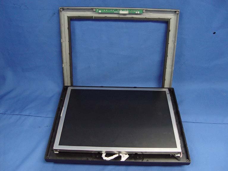
Page 9 SHENZHEN KSAI ELECTRONICS CO.,LTD 17" TFT-LCD Monitor FCC ID:KVCKS-17 Figure 7 Inside Configuration of the EUT Figure 8 Inside Configuration of the EUT Page 10 SHENZHEN KSAI ELECTRONICS CO.,LTD 17" TFT-LCD Monitor FCC ID:KVCKS-17 Figure 9 Frontside of the LCD Panel Figure 10 Backside of the LCD Panel Page 11 SHENZHEN KSAI ELECTRONICS CO.,LTD 17" TFT-LCD Monitor FCC ID:KVCKS-17 Figure 11 Label of LCD Panel Figure 12 Main Board, Component Side Page 12 SHENZHEN KSAI ELECTRONICS CO.,LTD 17" TFT-LCD Monitor FCC ID:KVCKS-17 Figure 13 Main Board, Component Side Figure 14 Power Board, Component Side Page 13 SHENZHEN KSAI ELECTRONICS CO.,LTD 17" TFT-LCD Monitor FCC ID:KVCKS-17 Figure 15 Power Board, Component Side Figure 16 Control Board, Component Side Page 14 SHENZHEN KSAI ELECTRONICS CO.,LTD 17" TFT-LCD Monitor FCC ID:KVCKS-17 Figure 17 Control Board, Component Side Figure 18 Adaptor Page 15 SHENZHEN KSAI ELECTRONICS CO.,LTD 17" TFT-LCD Monitor FCC ID:KVCKS-17 Figure 19 Label of the adaptor Figure 20 D-Sub Cable Page 16 SHENZHEN KSAI ELECTRONICS CO.,LTD 17" TFT-LCD Monitor FCC ID:KVCKS-17 Figure 21 Audio Cable Figure 22 AC Cable
Operational Description
Page 26 SHENZHEN KSAI ELECTRONICS CO.,LTD 17" TFT-LCD Monitor FCC ID:KVCKS-17 GTO TX's Technical Specifications Page 27 SHENZHEN KSAI ELECTRONICS CO.,LTD 17" TFT-LCD Monitor FCC ID:KVCKS-17 Page 28 SHENZHEN KSAI ELECTRONICS CO.,LTD 17" TFT-LCD Monitor FCC ID:KVCKS-17
Schematics
5 5 4 4 3 3 2 2 1 1 DD CC BB AA DVI CONNECTOR Near VGA pins ANALOG DDC DIGITAL DDC NC NC NC 1.0 1.Input connector C 15Monday, January 09, 2006 L-121A Title SizeDocument NumberRev Date:Sheetof A-HS A-GREENVGA_SDA VGA_SCL A-BLUE A-RED A-VS RX0+ RX1+ RX1- RX2+ RXC+ RX2- RX0- DDC_SDA_DVI DDC_SCL_DVI RXC- RED- GREEN+ DDC_SCL_VGA HSYNC BLUE+ VSYNC VGA_CAB BLUE- RED+ DDC_SDA_VGA GREEN- DVI_5V GND GND GND GND GND GND GND GND VGA_5V GND GND GND +5V GND +5V +5V GND C140.01uF C130.01uF R510K CN2 DB15 HD 1 6 2 7 3 8 4 9 5 11 12 13 14 15 10 S 1 S 2 C110.01uF C2 NC R810.0 1% U14D NC 98 C94 2K2 C150.01uF R15 10K R 2 2 7 5 R910.0 1% R12100 R 2 3 7 5 U14E NC 1110 R 2 5 8 4 . 5 C120.01uF R210.0 1% R7920.0 1% R770R U1 24AA02 4 81 2 3 7 6 5 GND VCCA0 A1 A2 WP SCL SDA R1847.0 1% U14F NC 1312 R1747.0 1% C9 0.1uF R10 10K R310.0 1% R780R R8020.0 1% CN1 DVI-D 1 2 3 4 5 6 7 8 9 10 11 12 13 14 15 16 17 18 19 20 21 22 23 24 34 33 RX2- RX2+ GND RX4- RX4+ SCL SDA VS RX1- RX1+ GND RX3- RX3+ 5V GND HP RX0- RX0+ GND RX5- RX5+ GND RXC+ RXC- Shell Shell R 2 4 8 4 . 5 U2 24AA02 4 81 2 3 7 6 5 GND VCCA0 A1 A2 WP SCL SDA R14 10K R2820.0 R110.0 1% R410.0 1% U14A NC 12 R2047.0 1% R 2 1 7 5 R2720.0 1% R610.0 1% C93 2K2 R11 10K C10 0.1uF C160.01uF R19100 U14B NC 34 R13100 R 2 6 8 4 . 5 R16100 R710.0 1% U14C NC 56 5 5 4 4 3 3 2 2 1 1 DD CC BB AA L B A D C _ R E T Close to respective power Pins Close to respective power Pins 1% Close to respective power Pins Close to respective power Pins RXE3+ RXE3- RXE2+ RXE2- RXE1+ RXE1- RXE0+ RXE0- RXEC+ RXEC- RXO3+ RXO3- RXO2+ RXO2- RXO1+ RXO1- RXO0+ RXO0- RXOC+ RXOC- 1.0 2.GM5621 C 25Monday, January 09, 2006 L-121A Title SizeDocument NumberRev Date:Sheetof UART_DO DDC_SCL_VGA PWM1 DDC_SDA_DVI UART_DI TCLK SPI_CLK DDC_SCL_DVI SPI_DI PPWR XTAL SPI_DO PWM0 DDC_SDA_VGA PBIAS SPI_CSn LED1 LV3_E_R2N LV2_E_G0N LV1_E_G1N LV0_E_G2N E_CLKN E_CLKP LV1_E_G1P LV0_E_G2P LV2_E_G0P LV3_E_R2P LV3_O_R2N LV2_O_G0N LV1_O_G1N LV0_O_G2N O_CLKN LV3_O_R2P LV1_O_G1P O_CLKP LV0_O_G2P LV2_O_G0P LBADC_IN LED2 UART_DI RESETn UART_DO RED- RX2+ RED+ RXC+ DDC_SDA_DVI Rx0+ BLUE+ DDC_SDA_VGA DDC_SCL_VGA VSYNC PWM0 RX0- DDC_SCL_DVI BLUE- PBIAS RX2- HSYNC GREEN+ RX1- GREEN- RXC- RX1+ PPWR PWM1 LV3_E_R2N LV2_E_G0N LV1_E_G1N LV0_E_G2N E_CLKN LV1_E_G1P LV0_E_G2P LV3_E_R2P LV2_E_G0P E_CLKP LV3_O_R2N LV2_O_G0N LV1_O_G1N LV0_O_G2N O_CLKN LV0_O_G2P LV1_O_G1P LV2_O_G0P O_CLKP LV3_O_R2P MUTE LED2 LED1 LBADC_IN SPI_3V3 GND GND 1.8V_DVDD GND GND 3.3V_DVDD GND 3.3V_DVDD 3.3V_AVDD GND GND +3.3V_VDD GND GND +5V GND GND 3.3VA_LV 3.3VA_LV GND 3.3V_DVDD 3.3VA_RPLL 1.8V_AVDD 3.3V_AVDD GND GND 3.3VA_RPLL +3.3V_VDD +1.8V_VDD 1.8V_DVDD GND GND 1.8V_AVDD GND GND SPI_3V3 3.3VA_RPLL3.3V_AVDD 3.3V_DVDDSPI_3V3 GND GNDGND +3.3V_VDD CN8 GPROBE TJC3-4A 1 2 3 4 C 5 6 0 . 1 u F C35 22pF Q9 MMBT3906 1 2 3 C43 0.1uF R 3 8 1 0 K C36 47uF/25V R42 10K X1 14.318 MHz C32 0.1uF C27 47uF/25V C29 0.1uF U10 MAX809 3 2 1 VCCGR R 3 4 1 0 K C47 0.1uF C41 0.1uF C45 0.1uF C30 0.1uF C22 47uF/25V L2 FERRITE BEAD C53 0.1uF R290R U3 GM5621 56 49 50 33 34 36 37 38 39 35 29 40 62 60 27 45 41 96 42 119 100 61 10 9 8 5 4 3 24 6 7 94 93 52 127 125 124 123 46 44 43 51 28 32 31 30 13 14 15 16 8 5 19 20 21 22 11 23 99 59 97 1 0 3 1 0 4 105 1 0 6 108 109 1 1 0 111 89 90 65 64 121 120 122 126 1 2 8 57 58 63 66 67 69 72 73 75 76 80 81 83 84 1 0 7 112 113 114 115 12 6 4 8 1 7 5 5 1 1 8 8 7 9 5 9 8 1 0 2 9 1 1 1 6 5 3 1 0 1 9 2 8 2 7 4 22 5 4 7 6 8 7 1 7 7 7 9 8 6 7 8 7 0 1 8 5 4 8 8 1 1 7 12 GPO_1 PBIAS PWM0/GPO_4 O_CLKP_LV O_CLKN_LV O_CH2N_LV O_CH1P_LV O_CH1N_LV O_CH0P_LV O_CH2P_LV RESERVED O_CH0N_LV SPI_DO SPI_CLK RESERVED RESERVED RESERVED GREEN+ RESERVED PWM1/GPO_5 RED- SPI_DI E_CLKN_LV E_CLKP_LV E_CH3N_LV RESERVED RESERVED RESERVED RESERVED RESERVED E_CH3P_LV BLUE- BLUE+ CRVSS PPWR GPIO_13 GPIO_12 GPIO_11 RESERVED RESERVED RESERVED GPO_0 RESERVED O_CH3N_LV O_CH3P_LV RESERVED E_CH1P_LV E_CH1N_LV E_CH0P_LV E_CH0N_LV A V S S _ D V I RESERVED RESERVED RESERVED RESERVED E_CH2P_LV RESERVED RED+ SPI_CSn GREEN- A V S S _ A D C A V D D _ A D C _ 1 8 VBUFC_RPLL V D D _ R P L L _ 1 8 XTAL TCLK A V D D _ R P L L _ 3 3 RESETn HSYNC VSYNC DDC_SDA_VGA DDC_SCL_VGA GPIO_9 GPIO_8 GPIO_10 GPIO_14 A V D D _ B I A S _ 3 3 GPO_2 GPO_3 RVDD_33 DDC_SCL_DVI DDC_SDA_DVI REXT RX2+ RX2- RX1+ RX1- RX0+ RX0- RXC+ RXC- V S S _ R P L L LBADC_VSS LBADC_IN3 LBADC_IN2 LBADC_IN1 A V S S _ B I A S V S S _ O U T V S S _ O U T C V D D _ 1 8 C V D D _ 1 8 C V D D _ 1 8 C V D D _ 1 8 A V S S _ A D C A V S S _ A D C A V S S _ A D C R V D D _ 3 3 L B A D C _ V D D _ 3 3 R V D D _ 3 3 A V D D _ A D C _ 3 3 A V D D _ A D C _ 3 3 A V D D _ D V I _ 3 3 A V D D _ D V I _ 3 3 V D D _ O U T _ 3 3 V D D _ O U T _ 3 3 V D D _ O U T _ 3 3 A V S S _ D V I A V S S _ D V I A V S S _ D V I A V S S _ D V I A V D D _ D V I _ 1 8 A V D D _ D V I _ 1 8 A V D D _ D V I _ 1 8 C R V S S C R V S S C R V S S C R V S S E_CH2N_LV C57 0.1uF C37 0.1uF C33 0.1uF C42 0.1uF C40 47uF/25V C26 0.1uF C34 22pF C44 0.1uF L1 FERRITE BEAD L4 FERRITE BEAD C28 0.1uF C31 0.1uF R53 4K7 C25 0.1uF C51 0.1uF C23 0.1uF L5 FERRITE BEAD C39 0.1uF C49 0.1uF R31250.0 U4 SST25VF010 1 2 3 45 6 7 8 CE# SO WP# VSSSI SCK HOLD# VCC C52 0.1uF C50 0.1uF L3 FERRITE BEAD R54 10K C55 220pF R324K7 C46 0.01uF C24 0.1uF R 4 1 8 2 0 K C38 47uF/25V R43 10K R3310K 5 5 4 4 3 3 2 2 1 1 DD CC BB AA 0.8A-max 3A-max 1.0 3. Output and Power C 35Monday, January 09, 2006 L-121A Title SizeDocument NumberRev Date:Sheetof LED2 LED1 BKLT_ADJ GND +12V +12V BKLT_EN PWM0 PBIAS LED2 LED1 LBADC_IN GND +5V GND +5V GND GNDGND +12V GND GND +5V GNDGNDGND GND GND +1.8V_VDD GND GND GND +3.3V_VDD +5V GND +5V GND GND +3.3V_VDD GND C66 47uF/25V C65 0.1uF C59 0.1uF U5 LM1117MPX-3.3 TO-252 1 32 4 GND VINVOUT TAB R425K6 R57 220R R4315K R36820 C67 0.1uF C61 47uF/25V R82 1K L633uH C62 10uF/16V D22 IN4148 12 R591K Q5 MMBT3904 1 2 3 R56 220R C64 470uF/16V R354K7 C58 47uF/25V C60 0.1uF CN14 POWER Q2 MMBT3904 3 1 2 D24 SK34 2 1 C63 0.1uF C70 470uF/16V R581K U6 LM1117MPX-1.8 TO-252 1 32 4 GND VINVOUT TAB R371K C69 47uF/25V R39…
Text truncated - open the document above for the full version.
Test Report
FCC ID:KVCKS-17 Audix Technology (Shenzhen) Co., Ltd. Report No. ACS-F07279 APPLICATION FOR CERTIFICATION On Behalf of SHENZHEN KSAI ELECTRONICS CO.,LTD 17" TFT-LCD Monitor Model Number: KS17 Prepared for : SHENZHEN KSAI ELECTRONICS CO.,LTD 31 ST FL,YIHAI SQUARE, CHUANGYE RD, NANSHAN DISTRICT SHENZHEN, GUANGDONG, CHINA Prepared By : Audix Technology (Shenzhen) Co., Ltd. No. 6, Ke Feng Rd., 52 Block, Shenzhen Science & Industrial Park, Nantou, Shenzhen, Guangdong, China Tel: (0755) 26639496 Report Number : ACS-F07279 Date of Test : Jun.21, 2007 Date of Report : Jul.02, 2007 FCC ID:KVCKS-17 Audix Technology (Shenzhen) Co., Ltd. Report No. ACS-F07279 TABLE OF CONTENTS Description Page Test Report Declaration 1. SUMMARY OF STANDARDS AND RESULTS .................................................................. 1-1 1.1. Description of Standards and Results.............................................................................................1-1 2. GENERAL INFORMATION .................................................................................................. 2-1 2.1. Description of Device (EUT) .........................................................................................................2-1 2.2. Tested Supporting System Details .................................................................................................2-1 2.3. Test Facility....................................................................................................................................2-3 2.4. Measurement Uncertainty ..............................................................................................................2-3 3. POWER LINE CONDUCTED EMISSION TEST................................................................ 3-1 3.1. Test Equipments.............................................................................................................................3-1 3.2. Block Diagram of Test Setup .........................................................................................................3-1 3.3. Power Line Conducted Emission Test Limits ................................................................................3-1 3.4. Configuration of EUT on Test .......................................................................................................3-2 3.5. Operating Condition of EUT..........................................................................................................3-2 3.6. Test Procedure................................................................................................................................3-2 3.7. Power Line Conducted Emission Test Results...............................................................................3-3 4. RADIATED EMISSION TEST ............................................................................................... 4-1 4.1. Test Equipment ..............................................................................................................................4-1 4.2. Block Diagram of Test Setup .........................................................................................................4-1 4.3. Radiated Emission Limit ................................................................................................................4-2 4.4. EUT Configuration on Test............................................................................................................4-2 4.5. Operating Condition of EUT..........................................................................................................4-3 4.6. Test Procedure................................................................................................................................4-3 4.7. Radiated Emission Test Results .....................................................................................................4-3 5. DEVIATION TO TEST SPECIFICATIONS ........................................................................ 5-1 6. PHOTOGRAPH........................................................................................................................ 6-1 6.1. Photos of Power Line Conducted Emission Test ...........................................................................6-1 6.2. Photos of Radiated Emission Test (In Anechoic Chamber) ...........................................................6-2 FCC ID:KVCKS-17 Audix Technology (Shenzhen) Co., Ltd. Report No. ACS-F07279 TEST REPORT CERTIFICATION Applicant : SHENZHEN KSAI ELECTRONICS CO.,LTD Manufacturer : SHENZHEN KSAI ELECTRONICS CO.,LTD EUT Description : 17" TFT-LCD Monitor (A) MODEL NO. : KS17 (B) SERIAL NO. : N/A (C) POWER SUPPLY : DC 12V Adaptor Input 120V/60Hz Test Procedure Used: FCC Rules and Regulations Part 15 Subpart B Class B 2006. The device described above is tested by Audix Technology (Shenzhen) Co., Ltd. to determine the maximum emission levels emanating from the device. The maximum emission levels are compared to the FCC Part 15 Subpart B Class B limits for radiated and conducted emissions. The test results are contained in this test report and Audix Technology (Shenzhen) Co., Ltd. is assumed full responsibility for the accuracy and completeness of tests. Also, this report shows that EUT is technically compliant with FCC requirements. This report applies to above tested sample only. This report shall not be reproduced in part without written approval of Audix Technology (Shenzhen) Co., Ltd. Date of Test : Jun.21, 2007 Prepared by : Sala Yang/ Assistant Reviewer : Iceman Hu / Senior Engineer Approved & Authorized Signer : Ken Lu / Deputy Manager FCC ID:KVCKS-17 Page Audix Technology (Shenzhen) Co., Ltd. Report No. ACS-F07279 1-1 1. SUMMARY OF STANDARDS AND RESULTS 1.1. Description of Standards and Results The EUT have been tested according to the applicable standards as referenced below. EMISSION Description of Test ItemStandard Limits Results Power Line Conducted Emission Test FCC Part 15: 2006 ANSI C6…
Text truncated - open the document above for the full version.
Test Setup Photos
FCC ID:KVCKS-17 Page 6-1 Audix Technology (Shenzhen) Co., Ltd. Report No. ACS-F07279 6. PHOTOGRAPH 6.1. Photos of Power Line Conducted Emission Test FCC ID:KVCKS-17 Page 6-2 Audix Technology (Shenzhen) Co., Ltd. Report No. ACS-F07279 6.2. Photos of Radiated Emission Test (In Anechoic Chamber) FCC ID:KVCKS-17 Page 6-3 Audix Technology (Shenzhen) Co., Ltd. Report No. ACS-F07279
Contact Information
Applicant
Tan Zhi Sheng
086 0755-6646144Fax: 086 0755-6408859
Technical Contact
Audix TechnologyKen Lu
[email protected]86-755-2663-9497
No. 6 Ke Feng Rd. 52 Block · Shenzhen · China
Test Firm
Audix Technology (Shenzhen) Co., Ltd.Smart Tsai
Technical Specifications
| # | Rule Parts | Frequency Range | Power Output |
|---|---|---|---|
| 1 | 15B | - | - |
Other Applications from Ksai Electronics Co Ltd
KVCKS-15
Jul 05, 200715" TFT-LCD Monitor
Equipment Class
JBP - Part 15 Class B Computing Device Peripheral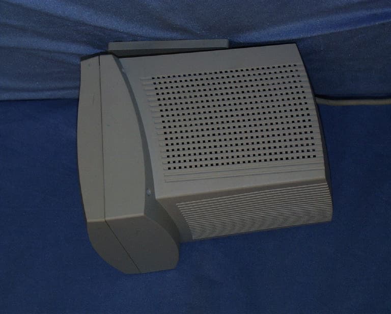
KVCKS-C156
Aug 21, 200110" COLOR MONITOR WITH MAX RESOLUTION 1024X768(48K
Equipment Class
JBP - Part 15 Class B Computing Device Peripheral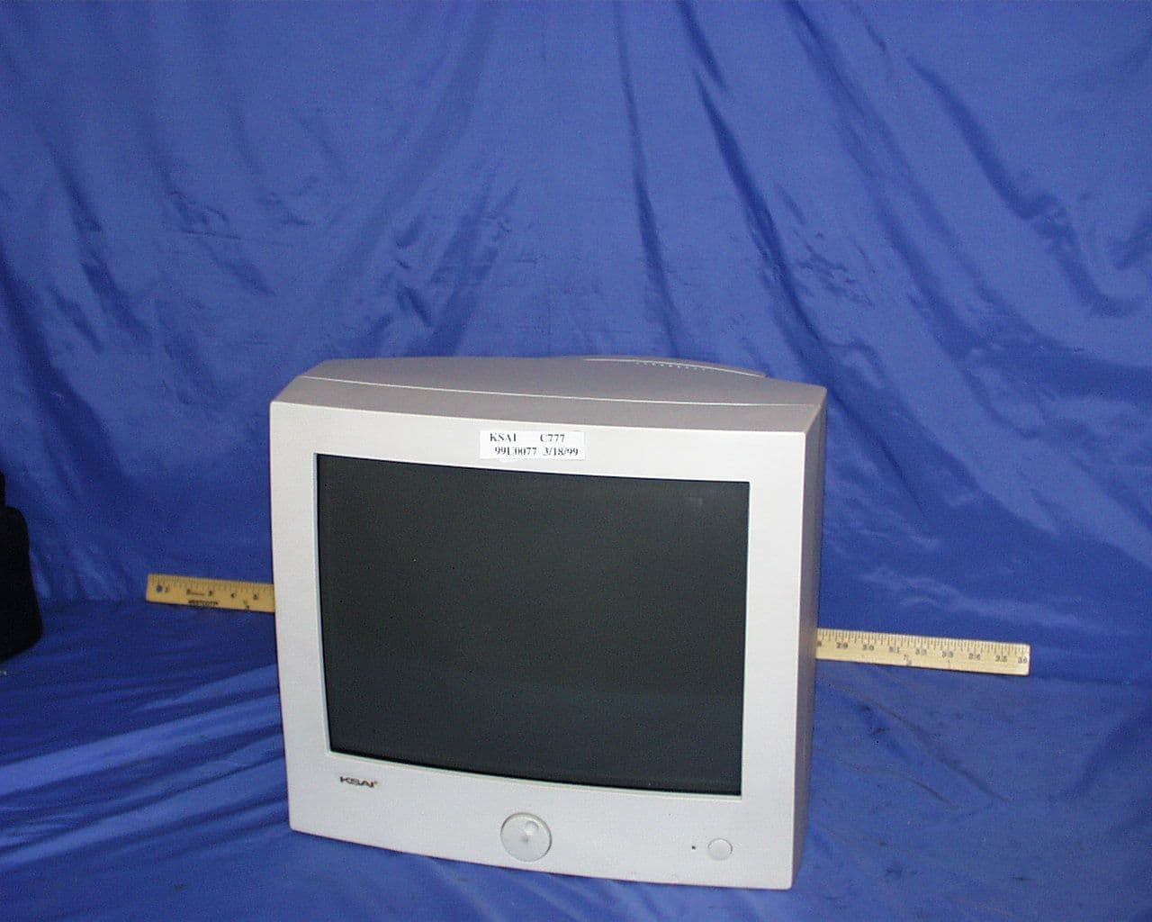
KVCKS-77
May 31, 1999JBP - Part 15 Class B Computing Device Peripheral
Equipment Class
JBP - Part 15 Class B Computing Device Peripheral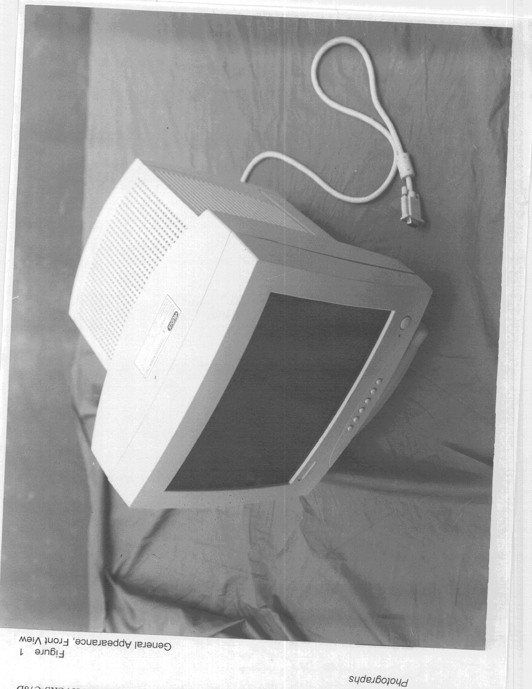
KVCKS-C78D
Oct 07, 1998JBP - Part 15 Class B Computing Device Peripheral
Equipment Class
JBP - Part 15 Class B Computing Device PeripheralKVCKS-CT1448
Mar 17, 1998JBP - Part 15 Class B Computing Device Peripheral
Equipment Class
JBP - Part 15 Class B Computing Device Peripheral