L3M859Pager
Swissphone Wireless AG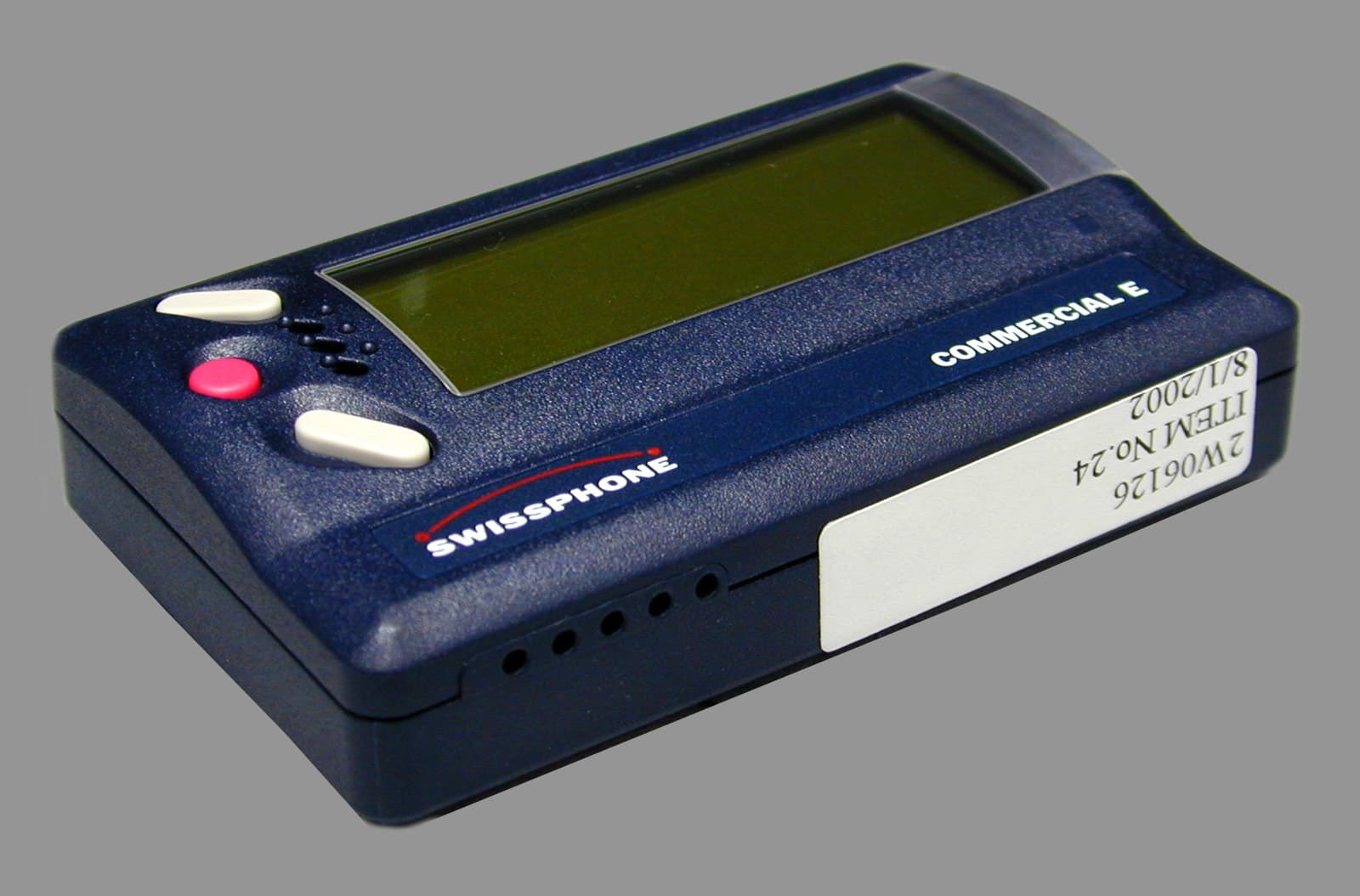
Click to zoom
Application Details
- Equipment Class
- CXX - Communications Rcvr for use w/ licensed Tx and CBs
- Date of Grant
- Dec 04, 2002
- Application Purpose
- Original Equipment
- Date of Application
- Dec 04, 2002
- Equipment Note
- Pager
- Frequency Range
- 430.00000000 - 470.00000000
- Company
- Swissphone Wireless AG
- Country
- Switzerland
Documents & Files
Document Text
Text extracted from the exhibit documents filed with the FCC. Open a document above to read the original.
Users Manual
User manual DE 506 PMD 000 098 08/02 Page 1/16 User Manual DE 506 Preface Congratulations on the purchase of your new pager. You will find it excels in its performance and user friendly features. The three key concept together with built in help information for each icon ensures that your pager is extremely simple to use. Despite it's ease of use, it is however recommended to read this manual carefully. You will always find the pager to be your loyal companion. WARNING • Do not operate this product in hazardous atmosphere or explosion risk areas. • Do not open device or remove labels * This device complies with Part 15 of the FCC Rules. Operation is subject to the following two conditions: (1) This device may not cause harmful interference, and (2) This device must accept any interference received, including interference that may cause undesired operation. Made in Switzerland WARNING Changes or modifications not expressly approved by the party responsible for compliance could void the user's authority to operate the equipment. User manual DE 506 PMD 000 098 08/02 Page 2/16 User manual DE 506 PMD 000 098 08/02 Page 3/16 Contents 1. Putting into Operation your pager ....................................................................... 2 2. Overview ............................................................................................................. 3 3. Standby Mode..................................................................................................... 3 4. Message Icons Display ....................................................................................... 4 4.1. Selecting a Message ............................................................................. 4 4.2. Reading Messages................................................................................ 4 4.2.1. Extending Display Time ........................................................... 4 4.3. Symbol : Automatic Message File ........................................................ 5 4.4. Symbol : Personal Message File .......................................................... 6 5. Status Symbols ................................................................................................. 7 6. Menu ................................................................................................................. 7 6.1. Programming option: Simplified Operation............................................ 7 6.2. Menu Symbol: Display Text: "Back ?" .................................................. 8 6.3. Menu Symbol: Display Text: "File message ?"..................................... 8 6.4. Menu Symbol: Display Text: "Delete message ?" ................................ 8 6.5. Menu Symbol: Display Text: "Protect message ?" ............................... 8 6.6. Menu Symbol: Display Text: "Set clock ?"............................................ 9 6.7. Menu Symbol: Display Text: "Set alarm clock ?".................................. 9 6.8. Menu Symbol: Display Text: "Silent ?" ................................................. 9 6.9. Menu Symbol: Display Text: "Loud ?" .................................................. 9 6.10. Menu Symbol: Display Text: "Submenu ?"......................................... 10 6.11. Menu Symbol: Display Text: "Turn off ?"............................................ 10 6.12. Switching on ........................................................................................ 10 7. Sub-menu ........................................................................................................... 10 7.1. Volume .................................................................................................. 11 7.2. Sleep Mode ........................................................................................... 13 7.3. Clock System ........................................................................................ 13 7.4. Snoozer ................................................................................................. 14 7.5. Acoustic "Out of range" Warning........................................................... 14 7.6. Acoustic Call Reminder ......................................................................... 14 7.7. Message-Font ....................................................................................... 15 7.8. Language .............................................................................................. 15 7.9. Battery................................................................................................... 15 8. Interface/Periphery ............................................................................................. 16 8.1. Accessories ........................................................................................... 16 User manual DE 506 PMD 000 098 08/02 Page 4/16 1. Putting into Operation your pager Power Supply Energy Source:Type:Operation Time : Alkaline BatteryLR 6, 1,5 Vapprox. 1500 hours. Accu Nickel Cadmium (rechargeable)600 mAh, AA, 1,2 Vapprox. 370 hours. Accu Nickel Metal Hydrid (rechargeable) 1000 mAh, AA, 1,2 V approx. 680 hours. Inserting the battery - Pull the securing pin (1) upwards. - Remove the battery cover (2) by sliding it in the direction of the arrow. - Insert the battery (3) and ensure correct polarity ( + / - ). - The pager switches on automatically (display, vibrator). - Replace the cover (2). - Push the securing pin (1) downwards gently. - Set the clock (see section 6.5.). Battery 1.5V or Accu 1.2V + 3 2 1 User manual DE 506 PMD 000 098 08/02 Page 5/16 2. Overview - All operating functions can be carried out with the three keys: upper key (1) middle key (2) lower key (3) Menu icons (see section 6) select with upper key (1) Message icons (see section 4) select with lower key (3) Status symbols (see section 5) 3. Standby Mode - If the keys are not used within 16 sec., the pager automatically switches over to standby mode: 14:47 number of unread messages 2 10.JAN.1995 …
Text truncated - open the document above for the full version.
Users Manual
1 Roosstrasse 53, 8832 Wollerau, Switzerland User Manual DE516C DE532C DE516C Ex 2 Contents 1Putting your pager into operation ........................................................................................................... 4 1.1Power supply .................................................................................................................................. 4 1.2Inserting the battery ........................................................................................................................ 4 2Standby mode........................................................................................................................................ 5 3Status display......................................................................................................................................... 6 3.1Display Illumination......................................................................................................................... 6 4Operating levels ..................................................................................................................................... 7 4.1Simple mode................................................................................................................................... 7 4.2Comprehensive Mode .................................................................................................................... 7 5Main menu ............................................................................................................................................. 8 5.1Key icons ........................................................................................................................................ 8 5.2Menu icons ..................................................................................................................................... 8 5.3Function icons ................................................................................................................................ 9 6Description of menu functions ............................................................................................................. 10 6.1Message menu ....................................................................................................................... 10 6.1.1General.................................................................................................................................. 10 6.1.2Read message ................................................................................................................. 11 6.1.3Delete message(s) ........................................................................................................... 11 6.1.4Save message ................................................................................................................. 11 6.1.5Switch RIC on and off .................................................................................................... 11 6.2Alert group .............................................................................................................................. 12 6.2.1Loud alert ......................................................................................................................... 12 6.2.2Mini beep ......................................................................................................................... 12 6.2.3Silent alert ........................................................................................................................ 12 6.2.4Vibrator on/off ................................................................................................................... 12 6.2.5Light on/off ....................................................................................................................... 12 6.2.6Set alert pattern ................................................................................................................. 12 6.2.7Acoustic out of range ....................................................................................................... 12 6.3Time menu ............................................................................................................................. 12 6.3.1Set time ............................................................................................................................ 12 6.3.2Set alarm clock ................................................................................................................ 13 6.4Special menu ......................................................................................................................... 13 6.4.1Switch off ......................................................................................................................... 13 6.4.2Bold font on/off or choose character set .......................................................................... 13 6.4.3Selecting the menu language .......................................................................................... 13 6.4.4Status information ............................................................................................................ 13 7Interface / Periphery............................................................................................................................. 14 7.1Accessories .................................................................................................................................. 14 3 Preface Congratulations on the purchase of your new POCSAG/ERMES pager. We are sure that you will appreciate its high performance and user friendly features. The operating concept together with its built-in help information for each icon ensures that your pager is extremely simple to use. Despite of its easy operation, it is recommended that you should read this manual carefully. Swissphone's alphanumeric pagers can be configured with many different options. The user manual cover…
Text truncated - open the document above for the full version.
Block Diagram
Service Manual DE 506 PMD 000 098 12/96 chapter 4 Page 3/9 4.1.2. RF-Block Diagram fo nfo PREAMP fe = nfo PHASE 90 º 0 º MIXER I MIXER Q AMP Q AMP I DEMOD UAA2080H IC 1 DATA PIN 3 GND Vdd2 ECO PIN 4 SHIFTER A1 Q1 Q I The radio signal received over antenna (A1) is amplified internally in IC1 (differential input) and is split thereafter in a phase shifter into two signals 90° apart from each other. Both the signals are mixed in two identical mixers in IC1 with a local oscillator, which lies with Direct Conversion principle directly on the reception frequency (n*fo = fe). The quartz Q1 oscillates at a lower frequency. The output signal of the quartz is multiplied by n in relation to the Reception Frequency (see chapter 4.2.2 Oscillator). Both the signals (I and Q) gained after the mixing, are in AF range and are still phase shifted by 90°. They are filtered within IC1 (necessary gap from neighbouring channels), amplified further, limited and lead to a quadrature demodulator. The output signal at pin3 corresponds to the digital DFSK-POCSAG signal which is lead to the Digital Part for further processing. The DC-IC is switched off through the Economizer Signal (ECO) in certain time intervals in order to save battery power.
Block Diagram
Technical Description DE516C Pag e 17/18 3 HF Stage 3.1 Block Diagram Blockdiagramm DE 516 Ex, Mainmodul Analogteil HF-Interface Analog-Bus VRX file: hfblock.drw A fe=nfo IC1 UAA2080H PREAMP MIXER I MIXER Q AMP Q AMP I DEMOD nfo fo nfo Q1 EC DO 90° 0° PHASE-SHIFTER 3.1.1 Summary The HF stage is implemented by a direct conversion chip from Philips. This chip converts the HF signal directly into a digital stream of data. 3.1.2 Aerial / Preamplifier (LNA) Two alternative aerial types can be fitted, depending on the pager. The ferrite aerial can receive frequencies up to 200 MHz. A frame aerial is necessary for higher frequencies. The components C4, C5 and C6 are used to adapt the aerial properties to the IC UAA2080H. A coupling using C1, L1 and C3 has been provided to enable the attachment of an external aerial to the pager. L2, L3 and C22 form the output tuned circuit of the LNA. The necessary supply voltage for the LNA is fed via L2 and L3. The gain of the LNA is adjusted with R1. 3.1.3 Phase Shifter with Adaptation The output signal of the LNA is picked symmetrically off the C22 and decoupled via C23, C24 and C27. C27 assists in the impedance transformation. The signal is then split into two paths that are shifted by +45° and -45° respectively to the signal received. Because of the balancing, these splits are present in duplicate (C26 / L4 and C25 / L5).
Cover Letter(s)
From: "Ruby Dulmage" <[email protected]> To: "Curtis-Straus TCB" <[email protected]> Sent: Wednesday, October 30, 2002 11:38 AM Attach: InstructionsDE516CV1.4.pdf; Differences DE506_DE516c.pdf; 2E_DE506_USA.pd f Subject: Reply: Swissphone FCC ID: L3M859 Page 1 of 1 12/5/2002 Hi Barry: Please see answers under your questions and also attachments. I trust this information will enable you to complete this submissions. Thanks, Ruby ----- Original Message ----- From: Curtis -Straus TCB To: Ruby Dulmage Sent: Monday, October 14, 2002 7:24 PM Subject: Swissphone FCC ID: L3M859 Hi Ruby, We have identified these issues following our review of the application: 1. Please supply a detailed comparison of the two models you wish to be certified under the same FCC ID. Please see attached Differences in models. 2. The user manuals do not contain the 15.21 statement. Please see attached revised user manuals 3. Please justify why the C63.4 clause 12.1.1 procedure was not followed in each of the frequency bands. The samples sent were fixed frequencies. Thus customer has stated that all receivers are identical from an RF standpoint accross all bands. Receiver characterization was determined on one same sent to use (no emissions detected at 3m). See notes on page 4 of test report. 4. How was the device stimulated? See C63.4 clause 12.1.1.2. The receiver was cohered using a CW tone as per ANSI C63.4 para 12.1 5. Over what frequency range was the radiated emissions taken. Please supply a data table. The receiver was searched from 30 MHz to the 10tarmonic of the L.O. as per the limit table on page 6 of the test report. Best regards Barry C. Quinlan Certification Manager Curtis-Straus TCB
Cover Letter(s)
From: "Ruby Dulmage" <[email protected]> To: "Curtis-Straus Certification Dept." <[email protected]> Sent: Monday, December 02, 2002 3:29 PM Attach: 2W06126 Issue 2.PDF Sub ject: Re: Reply: Swissphone FCC ID: L3M859 Page 1 of 2 12/5/2002 Hi Barry: Attached is a revised (Issue 2) test report. Thanks Ruby ----- Original Message ----- From: Curtis -Straus Certification Dept. To: Ruby Dulmage Sent: Monday, November 04, 2002 1:08 PM Subject: Re: Reply: Swissphone FCC ID: L3M859 Hi Ruby, Issues 2,4 & 5 have been resolved. For issue 1 we would like to see some testing conducted on the DE506 as the digital portion of the pager does differ from the DE516C. For issue 3 we do need to see radiated emission results over 3 frequencies in each band as required by 15.31(m). Barry ----- Original Message ----- From: Ruby Dulmage To: Curtis -Straus TCB Sent: Wednesday, October 30, 2002 8:38 AM Subject: Reply: Swissphone FCC ID: L3M859 Hi Barry: Please see answers under your questions and also attachments. I trust this information will enable you to complete this submissions. Thanks, Ruby ----- Original Message ----- From: Curtis -Straus TCB To: Ruby Dulmage Sent: Monday, October 14, 2002 7:24 PM Sub ject: Swissphone FCC ID: L3M859 Hi Ruby, We have identified these issues following our review of the application: 1. Please supply a detailed comparison of the two models you wish to be certified under the same FCC ID. Please see attached Differences in models. 2. The user manuals do not contain the 15.21 statement. Please see attached revised user manuals 3. Please justify why the C63.4 clause 12.1.1 procedure was not followed in each of the frequency bands. The samples sent were fixed frequencies. Thus customer has stated that all receivers are identical from an RF standpoint accross all bands. Receiver characterization was determined on one same sent to use (no emissions detected at 3m). See notes on page 4 of test report. 4. How was the device stimulated? See C63.4 clause 12.1.1.2. The receiver was cohered using a CW tone as per ANSI C63.4 para 12.1 5. Over what frequency range was the radiated emissions taken. Please supply a data table. The receiver was searched from 30 MHz to the 10tarmonic of the L.O. as per the limit table on page 6 of the test report. Best regards Barry C. Quinlan Certification Manager Curtis-Straus TCB Page 2 of 2 12/5/2002
ID Label/Location Info
Pages:1/1 Date:09.09.02 Author: Urs Aebersold SWISSPHONE Label for DE506 and DE516C
Operational Description
Service Manual DE 506 PMD 000 098 12/96 chapter 4 Page 1/9 Technical Description DE 506 Contents 4. Technical Description ......................................................................................... 2 4.1. Introduction ........................................................................................... 2 4.1.1. General.................................................................................... 2 4.1.2. RF-Block Diagram ................................................................... 3 4.1.3. Digital part-Block Diagram ....................................................... 4 4.2. Functional Description RF- Part ............................................................ 5 4.2.1. RF-Chip ................................................................................... 5 4.2.2. Oscillator.................................................................................. 5 4.2.4. Economizer.............................................................................. 5 4.3. Functional Description of Digital-Module............................................... 6 4.3.1. POCSAG Decoder................................................................... 6 4.3.1.1. Addresses .................................................................. 6 4.3.1.2. Economizing of RF-Receiver part .............................. 6 4.3.1.3. EEPROM ................................................................... 6 4.3.2. Microprocessor ........................................................................ 7 4.3.3. DC/DC Converter .................................................................... 7 4.3.4. CMOS-RAM (Battery-supported)............................................. 7 4.3.5. Display-Driver .......................................................................... 7 4.3.5.1. Liquid Crystal Display (LCD) ...................................... 8 4.4. Periphery-Interface................................................................................ 9 4.4.1. General.................................................................................... 9 4.4.2. Pin connections ....................................................................... 9 Service Manual DE 506 PMD 000 098 12/96 chapter 4 Page 2/9 4. Technical Description 4.1. Introduction 4.1.1. General The Swissphone Information Pager DE 506 combines the most advanced technology with its compact form. The "Direct Conversion" DFSK POCSAG Paging Receiver is controlled by a CMOS - microprocessor and is fed either by 1.2V accumulator or by 1,5V dry battery. The receiver contents two functional parts sandwiched and connected over 6-pin plug- socket connection. The Liquid Crystal Display (LCD) is fixed to the digital module with the help of a metal frame. Service Manual DE 506 PMD 000 098 12/96 chapter 4 Page 3/9 4.1.2. RF-Block Diagram fo nfo PREAMP fe = nfo PHASE 90 º 0 º MIXER I MIXER Q AMP Q AMP I DEMOD UAA2080H IC 1 DATA PIN 3 GND Vdd2 ECO PIN 4 SHIFTER A1 Q1 Q I The radio signal received over antenna (A1) is amplified internally in IC1 (differential input) and is split thereafter in a phase shifter into two signals 90° apart from each other. Both the signals are mixed in two identical mixers in IC1 with a local oscillator, which lies with Direct Conversion principle directly on the reception frequency (n*fo = fe). The quartz Q1 oscillates at a lower frequency. The output signal of the quartz is multiplied by n in relation to the Reception Frequency (see chapter 4.2.2 Oscillator). Both the signals (I and Q) gained after the mixing, are in AF range and are still phase shifted by 90°. They are filtered within IC1 (necessary gap from neighbouring channels), amplified further, limited and lead to a quadrature demodulator. The output signal at pin3 corresponds to the digital DFSK-POCSAG signal which is lead to the Digital Part for further processing. The DC-IC is switched off through the Economizer Signal (ECO) in certain time intervals in order to save battery power. Service Manual DE 506 PMD 000 098 12/96 chapter 4 Page 4/9 4.1.3. Digital part-Block Diagram RESET 3V-Li VDD LCD-BACKLIGHT DRIVERS LED RF-INTERFACE DC DC PERIPHERAL INTERFACE RAM M DECODER POCSAG- PROCESSOR MICRO- DISPLAY-DRIVER The serial data stream (POCSAG-Coding) with its corresponding transmission speed of 512, 1200 or 2400 Bits/s is evaluated by the decoder. The POCSAG decoder "PCF 5001T" also includes the EEPROM for RIC addresses and the pager configuration. The decoded signal is now passed over to the microprocessor (U1) in the blocks of four bits. The data are then structured and stored in 32kx8 full S-RAM (U2). In addition to that, in case of an incoming call or corresponding operation of the pager, the text data are sent to both LCD drivers situated on the Digital Module. The data are then displayed on the LCD. The operating voltage V DD of 3V is produced by a DC/DC converter. All the components are defined for this voltage, the only exception being the programming of EEPROMs (see chapter EEPROM). The RS-232 interface and the acknowledgement of the adaptation related to it, is supervised by the microprocessor ( see the description of periphery interface). The battery voltage V batt as well as the operational voltage V DD is constantly monitored by a voltage detector and the information is passed on to microprocessor for further processing and the corresponding signals are displayed whenever necessary (Low Battery alarm). The user can change the battery or recharge the accu, as the case may be. Service Manual DE 506 PMD 000 098 12/96 chapter 4 Page 5/9 4.2. Functional Description RF- Part 4.2.1. RF-Chip The whole processing on the RF-Stage is carried out by the RF-chip UAA2080H (IC1). The chip works on the principle of Direct Conversion. This means that the mix frequency of the local oscillator is identical to the reception frequency. The processing is carried out basically over symmetrical signals and not over ones referenced to Ground. Due…
Text truncated - open the document above for the full version.
Operational Description
Roosstrasse 53, 8832 Wollerau, Switzerland Technical Description DE516C Version 1.1 September 21, 2000/Kla Technical Description DE516C Pag e 2/18 List of Contents 1FUNCTION DESCRIPTION ....................................................................................................................... 3 1.1G ENERAL .................................................................................................................................................. 3 2DIGITALPRINT ........................................................................................................................................... 3 2.1D IGITAL S ECTION ..................................................................................................................................... 3 2.1.1Block Diagram................................................................................................................................. 3 2.1.2Miscellaneous buses ........................................................................................................................ 4 2.1.2.1Crete (decoder) bus ...................................................................................................................................... 4 2.1.2.2I2C bus......................................................................................................................................................... 6 2.1.2.3Interface bus................................................................................................................................................. 6 2.1.2.4Control bus .................................................................................................................................................. 7 2.1.2.5Address bus.................................................................................................................................................. 7 2.1.2.6Data bus ....................................................................................................................................................... 7 2.1.3Decoder ........................................................................................................................................... 8 2.1.3.1Description of the ports of the decoder SW95 (Crete) ................................................................................. 8 2.1.4 μ Controller ...................................................................................................................................... 9 2.1.4.1General......................................................................................................................................................... 9 2.1.4.2Miscellaneous lines...................................................................................................................................... 9 2.1.4.3Port 0 ........................................................................................................................................................... 9 2.1.4.4Port 1 ......................................................................................................................................................... 10 2.1.4.5Port 2 ......................................................................................................................................................... 10 2.1.4.6Port 3 ......................................................................................................................................................... 10 2.1.4.7Port 4 ......................................................................................................................................................... 10 2.1.4.8Port 5 ......................................................................................................................................................... 10 2.1.4.9Port 6 ......................................................................................................................................................... 11 2.1.4.10Port 7 ..................................................................................................................................................... 11 2.1.4.11Port 8 ..................................................................................................................................................... 11 2.1.5Static RAM (SRAM) ....................................................................................................................... 12 2.1.6EEPROM ....................................................................................................................................... 12 2.1.7Real Time Clock............................................................................................................................. 12 2.1.8Power-Management....................................................................................................................... 12 2.1.8.1DC/DC converter ....................................................................................................................................... 12 2.1.8.2Backup battery ...................…
Text truncated - open the document above for the full version.
Contact Information
Applicant
Andreas Manser(Product Manager)
Test Firm
Nemko Canada Inc.Stuart Beck
Technical Specifications
| # | Rule Parts | Frequency Range | Power Output |
|---|---|---|---|
| 2 | 15B | 430 MHz - 470 MHz | - |
Other Applications from Swissphone Wireless AG

L3M-ITC2800VHF
Sep 04, 2024VHF paging base station
Equipment Class
TNB - Licensed Non-Broadcast Station Transmitter
L3M-ITC2100-4B1
Oct 26, 2015POCSAG Paging Base Station
Equipment Class
TNB - Licensed Non-Broadcast Station Transmitter
L3M-ISITEIIIVHF
Sep 24, 2014one-way Paging-Transmitter
Equipment Class
TNB - Licensed Non-Broadcast Station Transmitter
L3M-ISITEIII530
Sep 24, 2014one-way Paging-Transmitter
Equipment Class
TNB - Licensed Non-Broadcast Station Transmitter
L3M-ISITEIIIUHF
Sep 24, 2014one-way Paging-Transmitter
Equipment Class
TNB - Licensed Non-Broadcast Station Transmitter