L3M876DE900 Receiver
Swissphone Wireless AG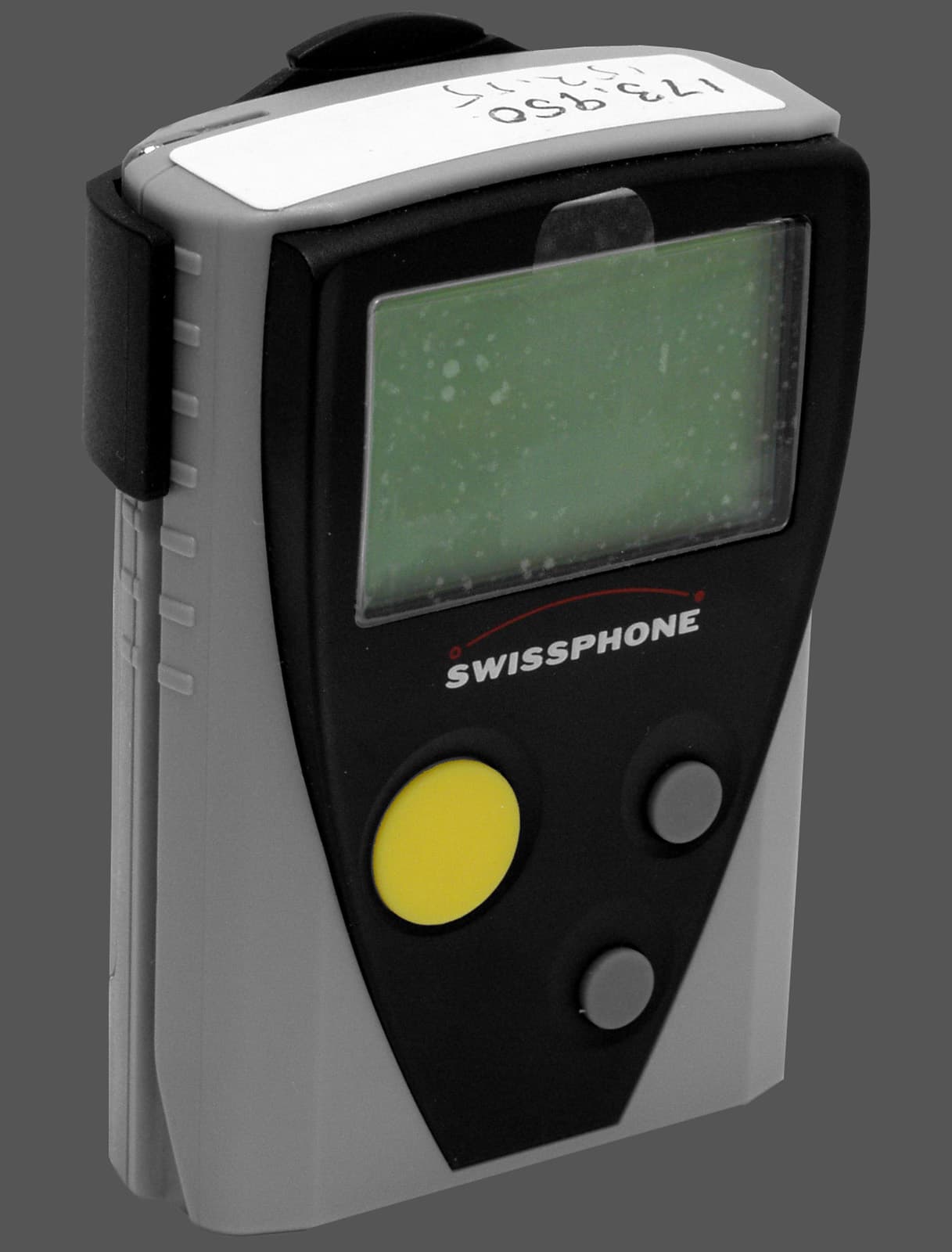
Click to zoom
Application Details
- Equipment Class
- CXX - Communications Rcvr for use w/ licensed Tx and CBs
- Date of Grant
- May 01, 2003
- Application Purpose
- Original Equipment
- Date of Application
- May 01, 2003
- Equipment Note
- DE900 Receiver
- Frequency Range
- 430.00000000 - 470.00000000
- Company
- Swissphone Wireless AG
- Country
- Switzerland
Documents & Files
Document Text
Text extracted from the exhibit documents filed with the FCC. Open a document above to read the original.
Users Manual
Operating Instructions SWISSPHONE DE900 Alphanumeric POCSAG pager 2 DECLARATION OF CONFORMITY We, SWISSPHONE Telecom AG, (name of the manufacturer) Roosstrasse 53, CH-8832 Wollerau, Switzerland Tel. +41 1/786 77 70, Fax +41 1/786 77 71 (Address) declare under our sole responsibility, that the product DE900 To which this declaration refers, complies with the following standards: ETS 300279, ETS 300390, EN 50081-1 / EN 50082-1 In accordance with the provisions of the guidelines 89/336EWG, 91/263EWG, 93/68EWG, R&TTE 99/05/EG Samstagern, June 1, 2002W. Schär / Manager Quality Control Regulatory Agency Compliance This device complies with Part 15 of the FCC Rules. Operation is subject to the following two conditions: (1) This device may not cause harmful interference, and (2) This device must accept any interference received, including interference that may cause undesired operation. Made in Switzerland WARNING Changes or modifications not expressly approved by the party responsible for compliance could void the user's authority to operate the equipment. 3 Preface We would like to congratulate you on your new receiver. With the purchase of the new SWISSPHONE DE900, you have decided on a device of the highest class. The SWISSPHONE DE900 receiver is distinguished by the combination of an attractive design, the most simple operation and the highest quality. The operating instructions provide you with important information as to how to exploit your device to the fullest extent. Always keep it readily available for consultation. The SWISSPHONE DE900 receiver can be configured specific to the application. For this reason, it is possible, that functions described in these operating instructions are not available in your device. We would like to wish you a lot of enjoyment reading these operating instructions and when using your SWISSPHONE DE900 receiver. Special remark concerning additional and helpful supplementary functions. Warning WARNING • Do not operate this product in hazardous atmosphere or explosion risk areas. • Do not open device or remove labels 4 Display Battery condition indication No field strength New message Loud alerting Silent alerting Alarm clock on Clock Menu text Position of the menu selection Further menus Push scroll key to select the next menu 5 Keys Switching the Receiver On By inserting the battery (refer to Changing the Power Source), the SWISSPHONE DE900 receiver is automatically switched on. Confirmation key (read messages, con- firm alarm, confirm selection) Scroll key (display main menu, scroll through menus and messages, change settings) Return key (alternately display user – and status information, leave selected menu or selected message) 6 Menu Structure By pushing the confirmation key, directly the message selection for the 'Read messages' is displayed (boldface frame). When pushing the scroll key, the main menu is displayed (boldface broken line frame) Main menu1st Sub-menu2nd Sub-menu MESSAGES Read Message selection Delete Delete all Message selection ALARMELoud Silent ALARM CLOCKOn / Off Set Repeat STATUS SETTINGS Clock Date Language SWITCH OFFAre you sure ? Scroll key Confirmation key Return key ProtectMessage selection User information Status display Accu Call reminder ALARM OPTIONSAlert pattern 7 Messages Read Messages A newly received message appears on the display immediately. - The alerting is stopped by pushing any key. - By pushing the scroll key, you can read the message. Only once you have scrolled right through to the end of the message it is considered as read. After the release time, the receiver reverts to the stand-by mode. Read Message Point of departure : Stand-by mode - Push the confirmation key and the menu selection is displayed, whereby the cursor is positioned on the most recent message. Main address Sub-address Time and date of the message received Start of the message Unread message with priority Unread message Protected message Free memory space Cursor Read messages 8 - Push the scroll key to select a message. - Push the confirmation key to read the selected message. The first 3 lines of the message are displayed. - Push the scroll key to read the whole message. Read all messages with the confirmation key You have the possibility of directly scrolling through - and reading all messages with the confirmation key. Simple operation If your receiver is configured for simple operation, then you directly get to the most recent message with the confirmation key. As soon as you have read it, the next unread message is displayed. In order to reach the main menu, push the scroll key and the return key simultaneously for at least 2 seconds. Display illumination In order to switch on the display illumination, push the confirmation key for 2 seconds. Push the confirmation key again for 2 seconds to switch the display illumination off again. At the latest when the receiver reverts back to the stand-by mode, the display illumination is automatically switched off. Deleting an Individual Message Point of departure : Stand-by mode - Push the scroll key and the menu ‘MESSAGES’ is displayed. - Push the confirmation key. - With the scroll key, select the menu ‘Delete messages’ and push the confirmation key. - With the scroll key select the message, which is to be deleted. - Push the confirmation key to delete the message. Deleting All Messages Point of departure : Stand-by mode - Push the scroll key and the menu ‘MESSAGES’ is displayed. - Push the confirmation key. - With the scroll key, select the menu ‘Delete all messages’ to delete all messages. - Push the confirmation key. - The question ‘Are you sure?’ is displayed. - Push the confirmation key to delete all messages or the return key to abort the process. 9 Protecting Messages Point of departure : Stand-by mode - Push the scroll key and the menu ‘MESSAGES’ is displayed. - Push the confirmation key. - With the scroll key, select the menu ‘Protect messages’. - Push the confirmation key. - Select the requ…
Text truncated - open the document above for the full version.
Block Diagram
copy rights byTechnical Description DE900 / Technische Funktionsbeschreibung DE900 V1.2_ENPage 1/12 PMD/D000 128Version 1.2 / 14.10.02 Technical Description DE900 Version 1.2 5 th September, 2002/BJ copy rights byTechnical Description DE900 / Technische Funktionsbeschreibung DE900 V1.2_ENPage 2/12 PMD/D000 128Version 1.2 / 14.10.02 Technical Function Description DE900 The most important functions of the main subassemblies of the DE 900 are described in the following. A functional unit consists of the mainboard and the LCD module with a keypad board. The DE 900 is characterised by a POCSAG protocol receiver which is based on the double superheterodyne principle. This means that the high frequency input signal is converted to the wanted signal via two intermediate frequencies. Table of contents: copy rights byTechnical Description DE900 / Technische Funktionsbeschreibung DE900 V1.2_ENPage 3/12 PMD/D000 128Version 1.2 / 14.10.02 1. Block Diagram 1.1. Message Signal Reception • The received message signal is transmitted via the antenna to the high-frequency (HF) section • The LNA (low-noise amplifier) both filters and amplifies the signal there • The 1st mixer converts the filtered high frequency signal to a 21.4 MHz IF signal • The 21.4 MHz filter separates the wanted IF from the other combination frequencies • The 2nd mixer converts the filtered high frequency signal to a 2 MHz IF • Re-filtering • The threshold amplifier prepares the IF signal for demodulation • The demodulator processes the signal using an external resonator • The now-activated LF filter (Sallen & Key) is baud rate dependent and is switched by the microprocessor • The comparator generates a clean 0V / 3V signal formatted in the POCSAG protocol • This signal is then deciphered by the decoder and forwarded to the microprocessor via a serial interface • In the case of message signal comparison (e.g. the RIC had already received a recently sent message) ! communication with EEPROM • In normal operation, however, an instantaneous alarm is triggered • ! Beep ! Vibrator ! Display illumination ! Message display • In the terminal step, the message is saved in the EEPROM copy rights byTechnical Description DE900 / Technische Funktionsbeschreibung DE900 V1.2_ENPage 4/12 PMD/D000 128Version 1.2 / 14.10.02 copy rights byTechnical Description DE900 / Technische Funktionsbeschreibung DE900 V1.2_ENPage 5/12 PMD/D000 128Version 1.2 / 14.10.02 2. MAINBOARD The mainboard is constructed of a 4-layer multilayer circuit board and is fitted with SMD components. To optimise reception, the circuit board is divided in two subsections: the HF section and the digital section. 2.1. Power Supply The power supply is provided by means of the rechargeable battery (1.26 V nominal) or a conventional battery. The following power supply voltage range is required by the mainboard. BAT+ = 1.26 V/DCfor IF section, DC/DC converter, vibrator, beeper, voltage monitoring and regulation V DD = 3 V DC for microprocessor, decoder, EEPROM and LCD module 2Vin =2.5 V/DCfor LCD illumination V+ = 1 V/stab.for HF transistors V DD voltages = 3 V, 2Vin and V+ = 1 V are generated by the receiver itself via the DC/DC converter and the IF-IC. If the rechargeable battery voltage drops below 1.18 V, the battery alarm is triggered via the microprocessor (rhythmic clicking). Counting from this moment on, the device is still operational for approx. 24 hours more. If the voltage drops below 1 V/DC, the microprocessor resets and the device is switched off. NiMH, NiCad rechargeable batteries or dry cell batteries can be used as power supply sources. Please note that when non-rechargeable batteries are used, the receiver recognises these as such and no recharging can take place. copy rights byTechnical Description DE900 / Technische Funktionsbeschreibung DE900 V1.2_ENPage 6/12 PMD/D000 128Version 1.2 / 14.10.02 2.2. Antenna / Amplifier / Filter The signal is coupled via ferrite antenna L1. C1, C2, C3 and C4 tune the antenna to the proper resonance. The signal is subsequently amplified by transistor level T1/T2, which functions as a cascode switch. The desired frequency band is selected by means of a coupled filter consisting of both parallel resonant circuits L11/C11/C12 and L14/C14/C15. 2.3. Quartz Crystal Oscillator The major component here is a Colpitts oscillator. The output circuit with components C20/C30/L22 is needed for selection of the oscillator signal. The collector circuit filters out the doubled quartz crystal frequency (second harmonic) for the 2m band. The oscillator signal is transferred to the mixer via coupling capacitor C24. The oscillator frequency lies in the 4m band. The frequency during 2m UB and 2m MB operation is 21.4 MHz higher than the receiving signal. In the 2m upper band, the oscillator frequency is 21.4 MHz lower than the receiving signal. 2.4. First Mixer Level / Filter Transistor T51 mixes the amplified antenna signal with the local oscillator signal and sends it to the first IF 21.4 MHz. Oscillator circuit L51/C52 represents the load resistance at this stage. The IF signal is filtered through the next quartz crystal filter F51. This filter selection serves the purpose of suppressing adjacent channel interference and image frequency interference. R51, L51 and C52 as well as R53, L52, C55 and the input capacitance of IC 61 form the necessary matching impedance for the quartz crystal filter. The IF signal is then transferred to IC61 via coupling capacitor C56. 2.5. IF-IC In the second mixer level, the wanted signal 21.4 MHz is converted to 455 kHz. Quartz crystal Q61 delivers the oscillator frequency 20.945 MHz. The conversion to 455 kHz is implemented in the IF module TA31145 (IC 61) integrated mixer. The signal is subsequently filtered and amplified. The amplifiers are integrated in the IF-IC, the external ceramic filter F61 filters and also determines the channel separation (25 kHz / 12.5 kHz) for the receiver. In the last step, quadrature demodulation c…
Text truncated - open the document above for the full version.
ID Label/Location Info
Bemerkungen:Kunde: Freigabe PM, Name:Dat. / Vis USA Gez.17.03.03str Freig. AeAe-Nr.DatumVis.AeAe-Nr.DatumVis.AeAe-Nr.DatumVis.DatumVisum TYPENPROGRAMM Seite 1 von 2 Digitalempfänger DE9000547507 Gehäuse-Oberteilgrau Geh.-Frontschwarz Schrift weiss Bogen rot Tastegrau Tastegelb Tastegrau Gehäuse-Unterteilgrau ohne Batteriedeckel Batteriedeckelgrau Typenschild Quarzabdeck- schild Bemerkungen:Kunde: Freigabe PM, Name:Dat. / Vis USA Gez.17.03.03str Freig. AeAe-Nr.DatumVis.AeAe-Nr.DatumVis.AeAe-Nr.DatumVis.DatumVisum TYPENPROGRAMM Seite 2 von 2 Digitalempfänger DE9000547507 Maske:T114 Schild:0319590 Maske: V100 Schild:0319509 Typenschild Verpackungsschild SWISSPHONE Type: DE900 Freq.:Space: RIC: IC: 4404A-876FCC ID: L3M876 S/N: C ID SWISSPHONE Type: DE900 Freq.: kHz Art.Nr.: IC: 4404A-876 FCC ID: L3M876 S/N:
Operational Description
copy rights byTechnical Description DE900 / Technische Funktionsbeschreibung DE900 V1.2_ENPage 1/12 PMD/D000 128Version 1.2 / 14.10.02 Technical Description DE900 Version 1.2 5 th September, 2002/BJ copy rights byTechnical Description DE900 / Technische Funktionsbeschreibung DE900 V1.2_ENPage 2/12 PMD/D000 128Version 1.2 / 14.10.02 Technical Function Description DE900 The most important functions of the main subassemblies of the DE 900 are described in the following. A functional unit consists of the mainboard and the LCD module with a keypad board. The DE 900 is characterised by a POCSAG protocol receiver which is based on the double superheterodyne principle. This means that the high frequency input signal is converted to the wanted signal via two intermediate frequencies. Table of contents: copy rights byTechnical Description DE900 / Technische Funktionsbeschreibung DE900 V1.2_ENPage 3/12 PMD/D000 128Version 1.2 / 14.10.02 1. Block Diagram 1.1. Message Signal Reception • The received message signal is transmitted via the antenna to the high-frequency (HF) section • The LNA (low-noise amplifier) both filters and amplifies the signal there • The 1st mixer converts the filtered high frequency signal to a 21.4 MHz IF signal • The 21.4 MHz filter separates the wanted IF from the other combination frequencies • The 2nd mixer converts the filtered high frequency signal to a 2 MHz IF • Re-filtering • The threshold amplifier prepares the IF signal for demodulation • The demodulator processes the signal using an external resonator • The now-activated LF filter (Sallen & Key) is baud rate dependent and is switched by the microprocessor • The comparator generates a clean 0V / 3V signal formatted in the POCSAG protocol • This signal is then deciphered by the decoder and forwarded to the microprocessor via a serial interface • In the case of message signal comparison (e.g. the RIC had already received a recently sent message) ! communication with EEPROM • In normal operation, however, an instantaneous alarm is triggered • ! Beep ! Vibrator ! Display illumination ! Message display • In the terminal step, the message is saved in the EEPROM copy rights byTechnical Description DE900 / Technische Funktionsbeschreibung DE900 V1.2_ENPage 4/12 PMD/D000 128Version 1.2 / 14.10.02 copy rights byTechnical Description DE900 / Technische Funktionsbeschreibung DE900 V1.2_ENPage 5/12 PMD/D000 128Version 1.2 / 14.10.02 2. MAINBOARD The mainboard is constructed of a 4-layer multilayer circuit board and is fitted with SMD components. To optimise reception, the circuit board is divided in two subsections: the HF section and the digital section. 2.1. Power Supply The power supply is provided by means of the rechargeable battery (1.26 V nominal) or a conventional battery. The following power supply voltage range is required by the mainboard. BAT+ = 1.26 V/DCfor IF section, DC/DC converter, vibrator, beeper, voltage monitoring and regulation V DD = 3 V DC for microprocessor, decoder, EEPROM and LCD module 2Vin =2.5 V/DCfor LCD illumination V+ = 1 V/stab.for HF transistors V DD voltages = 3 V, 2Vin and V+ = 1 V are generated by the receiver itself via the DC/DC converter and the IF-IC. If the rechargeable battery voltage drops below 1.18 V, the battery alarm is triggered via the microprocessor (rhythmic clicking). Counting from this moment on, the device is still operational for approx. 24 hours more. If the voltage drops below 1 V/DC, the microprocessor resets and the device is switched off. NiMH, NiCad rechargeable batteries or dry cell batteries can be used as power supply sources. Please note that when non-rechargeable batteries are used, the receiver recognises these as such and no recharging can take place. copy rights byTechnical Description DE900 / Technische Funktionsbeschreibung DE900 V1.2_ENPage 6/12 PMD/D000 128Version 1.2 / 14.10.02 2.2. Antenna / Amplifier / Filter The signal is coupled via ferrite antenna L1. C1, C2, C3 and C4 tune the antenna to the proper resonance. The signal is subsequently amplified by transistor level T1/T2, which functions as a cascode switch. The desired frequency band is selected by means of a coupled filter consisting of both parallel resonant circuits L11/C11/C12 and L14/C14/C15. 2.3. Quartz Crystal Oscillator The major component here is a Colpitts oscillator. The output circuit with components C20/C30/L22 is needed for selection of the oscillator signal. The collector circuit filters out the doubled quartz crystal frequency (second harmonic) for the 2m band. The oscillator signal is transferred to the mixer via coupling capacitor C24. The oscillator frequency lies in the 4m band. The frequency during 2m UB and 2m MB operation is 21.4 MHz higher than the receiving signal. In the 2m upper band, the oscillator frequency is 21.4 MHz lower than the receiving signal. 2.4. First Mixer Level / Filter Transistor T51 mixes the amplified antenna signal with the local oscillator signal and sends it to the first IF 21.4 MHz. Oscillator circuit L51/C52 represents the load resistance at this stage. The IF signal is filtered through the next quartz crystal filter F51. This filter selection serves the purpose of suppressing adjacent channel interference and image frequency interference. R51, L51 and C52 as well as R53, L52, C55 and the input capacitance of IC 61 form the necessary matching impedance for the quartz crystal filter. The IF signal is then transferred to IC61 via coupling capacitor C56. 2.5. IF-IC In the second mixer level, the wanted signal 21.4 MHz is converted to 455 kHz. Quartz crystal Q61 delivers the oscillator frequency 20.945 MHz. The conversion to 455 kHz is implemented in the IF module TA31145 (IC 61) integrated mixer. The signal is subsequently filtered and amplified. The amplifiers are integrated in the IF-IC, the external ceramic filter F61 filters and also determines the channel separation (25 kHz / 12.5 kHz) for the receiver. In the last step, quadrature demodulation c…
Text truncated - open the document above for the full version.
Test Report
Master: PT15-SubB-15109 Date: October 17, 2001 Test Report: 3W06967 Applicant: SWISSPHONE Telecom AG Roosstrasse 53 CH-8832 Wollerau Switzerland Equipment Under Test: SWISSPHONE DE900 (EUT) In Accordance With: FCC Part 15, Subpart B, 15.109 Tested By: Nemko Canada Inc. 303 River Road, R.R. 5 Ottawa, Ontario K1V 1H2 Authorized By: Russell Grant, Senior Technical Assessor Date: 29 April 2003 Total Number of Pages: 13 Nemko Canada Inc. FCC PART 15, SUBPART B, 15.109 PROJECT NO.:3W06967 EQUIPMENT: SWISSPHONE DE900 Page 2 of 13 Table Of Contents Section 1. Summary of Test Results .................................................................................. 3 Section 2. General Equipment Specification..................................................................... 5 Section 3. Radiated Emissions ............................................................................................ 6 Section 4. Block Diagrams ................................................................................................ 12 Section 5. Test Equipment List ........................................................................................ 13 Nemko Canada Inc. FCC PART 15, SUBPART B, 15.109 PROJECT NO.:3W06967 EQUIPMENT: SWISSPHONE DE900 Page 3 of 13 Section 1. Summary of Test Results General All measurements are traceable to national standards. These tests were conducted on a sample of the equipment for the purpose of demonstrating compliance with FCC Part 15, Subpart B. Measurement procedure ANSI C63.4-1992 was used for all tests. Radiated Emissions were measured on an open area test site. A description of the test facility is on file with the FCC. THIS TEST REPORT RELATES ONLY TO THE ITEM(S) TESTED. THE FOLLOWING DEVIATIONS FROM, ADDITIONS TO, OR EXCLUSIONS FROM THE TEST SPECIFICATIONS HAVE BEEN MADE. NONE See “ Summary of Test Data”. TESTED BY: ______________________________ DATE: 25 April 2003 Kevin Carr, EMC Specialist Nemko Canada Inc. authorizes the above named company to reproduce this report provided it is reproduced in its entirety and for use by the company’s employees only. Any use which a third party makes of this report, or any reliance on or decisions to be made based on it, are the responsibility of such third parties. Nemko Canada Inc. accepts no responsibility for damages, if any, suffered by any third party as a result of decisions made or actions based on this report. This report applies only to the items tested. Nemko Canada Inc. FCC PART 15, SUBPART B, 15.109 PROJECT NO.:3W06967 EQUIPMENT: SWISSPHONE DE900 Page 4 of 13 Summary Of Test Data Name Of Test Para. No. Results Antenna Conducted Emissions 15.111 N/A Radiated Emissions 15.109 Complied Powerline Conducted Emissions 15.107 N/A N/A’s: The EUT is Battery Power and has no accessible antenna port Test Conditions: Outdoor 27 March 2003 Temperature: 4°C Humidity: 70% 25 April 2003 Temperature: 1°C Humidity: 64% Nemko Canada Inc. FCC PART 15, SUBPART B, 15.109 PROJECT NO.:3W06967 EQUIPMENT: SWISSPHONE DE900 Page 5 of 13 Section 2. General Equipment Specification Manufacturer: Sprintel Communications AG (belongs to SWISSPHONE) Betriebsstätte Samstagern Fälmisstrasse 21 CH-8833 Samstagern Brand Name: SWISSPHONE DE900 Serial No’s.: 138.050MHz C200307.03535 155.050MHz C200307.03539 173.950MHz C200307.03542 400.050MHz C200306.02252 410.050MHz C200306.02251 419.950MHz C200306.02253 430.050MHz C200306.02254 450.050MHz C200306.02256 469.950MHz C200306.02257 Frequency Range: VHF 138 – 174 MHz UHF 400 – 420 MHz UHF 430 – 470 MHz Frequencies Tested: VHF 138.050, 155.050, 173.950 MHz UHF 400.050, 410.050, 419.950 MHz UHF 430.050, 450.050, 469.950 MHz Date Received In Laboratory: 26 March 2003 Nemko Identification No.: 1 - 9 Nemko Canada Inc. FCC PART 15, SUBPART B, 15.109 PROJECT NO.:3W06967 EQUIPMENT: SWISSPHONE DE900 Page 6 of 13 Section 3. Radiated Emissions Para. No.: 15.109(a) Test Performed By: Kevin Carr Date of Test: 27 March 2003, 25 April 2003 Minimum Standard: Frequency(MHz) Field Strength (dBμV/m @ 3m) 30 - 88 40.0 88 - 216 43.5 216 - 960 46.0 Above 960 54.0 Test Results: Complied. The device was verified for worst case emissions on 3 orthogonal axis. Measurement Data: See attached table. Nemko Canada Inc. FCC PART 15, SUBPART B, 15.109 PROJECT NO.:3W06967 EQUIPMENT: SWISSPHONE DE900 Page 7 of 13 Radiated Disturbance Test Data: 138 – 174 MHz Band Test Date: 27 March 2003 Engineer’s Name: Kevin Carr Temperature (C°): 4 Humidity %: 70 Tested as per (Table Top/Floor Standing): Table Top Test Distance (meters): 3 Dome: 1 Freq. (MHz) Ant. Pol. V/H RCVD Signal (dBμV) Ant. Factor (dB) Amp. Gain (dB) Cable Loss (dB) Field Strength (dBμV/m) Limit (dBμV/m) Margin (dB) Detector Amp. Low Freq. 159.4500 ED3 V 13.5 13.0 N/A 1.5 28.0 43.5 15.6 Q-Peak None 159.4500 ED3 H 14.5 12.4 N/A 1.5 28.4 43.5 15.1 Q-Peak None 318.9000 LP1 V 7.8 14.9 N/A 2.3 25.0 46.0 21.0 Q-Peak None 318.9000 LP1 H 7.9 15.3 N/A 2.3 25.5 46.0 20.6 Q-Peak None 478.3500 LP1 V 7.6 17.8 N/A 2.8 28.2 46.0 17.8 Q-Peak None 478.3500 LP1 H 7.4 18.0 N/A 2.8 28.3 46.0 17.8 Q-Peak None 637.8000 LP1 V 7.3 19.8 N/A 3.3 30.3 46.0 15.7 Q-Peak None 637.8000 LP1 H 7.3 20.7 N/A 3.3 31.3 46.0 14.8 Q-Peak None 797.2500 LP1 V 8.4 21.7 N/A 3.7 33.8 46.0 12.2 Q-Peak None 797.2500 LP1 H 7.5 22.5 N/A 3.7 33.7 46.0 12.3 Q-Peak None Mid. Freq. 176.4500 ED3 V 7.4 13.8 N/A 1.7 22.9 43.5 20.7 Q-Peak None 176.4500 ED3 H 6.5 13.1 N/A 1.7 21.3 43.5 22.3 Q-Peak None 352.9000 LP1 V 7.9 15.0 N/A 2.4 25.3 46.0 20.8 Q-Peak None 352.9000 LP1 H 7.9 15.3 N/A 2.4 25.6 46.0 20.4 Q-Peak None 529.3500 LP1 V 7.4 18.4 N/A 2.9 28.7 46.0 17.3 Q-Peak None 529.3500 LP1 H 7.5 19.0 N/A 2.9 29.4 46.0 16.6 Q-Peak None 705.8000 LP1 V 6.9 21.6 N/A 3.4 31.9 46.0 14.1 Q-Peak None 705.8000 LP1 H 7.0 21.8 N/A 3.4 32.3 46.0 13.8 Q-Peak None 882.2500 LP1 V 8.4 22.8 N/A 3.9 35.2 46.0 10.9 Q-Peak None 882.2500 LP1 H 8.5 23.6 N/A 3.9 36.0 46.0 10.0 Q-Peak None High Freq. 152.5500 ED3 V 16.1 12.5 N/A 1.5 30.1 43.5 13.4 Q-Peak None …
Text truncated - open the document above for the full version.
Test Setup Photos
Swissphone Set-Up Photo’s
Contact Information
Applicant
Andreas Manser(Product Manager)
Test Firm
Nemko Canada Inc.Stuart Beck
Technical Specifications
| # | Rule Parts | Frequency Range | Power Output |
|---|---|---|---|
| 3 | 15B | 430 MHz - 470 MHz | - |
Other Applications from Swissphone Wireless AG

L3M-ITC2800VHF
Sep 04, 2024VHF paging base station
Equipment Class
TNB - Licensed Non-Broadcast Station Transmitter
L3M-ITC2100-4B1
Oct 26, 2015POCSAG Paging Base Station
Equipment Class
TNB - Licensed Non-Broadcast Station Transmitter
L3M-ISITEIIIVHF
Sep 24, 2014one-way Paging-Transmitter
Equipment Class
TNB - Licensed Non-Broadcast Station Transmitter
L3M-ISITEIII530
Sep 24, 2014one-way Paging-Transmitter
Equipment Class
TNB - Licensed Non-Broadcast Station Transmitter
L3M-ISITEIIIUHF
Sep 24, 2014one-way Paging-Transmitter
Equipment Class
TNB - Licensed Non-Broadcast Station Transmitter