L9UUSHR-1900PCS Amplifier
Ace Antenna Company, Inc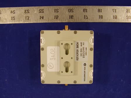
Click to zoom
Application Details
- Equipment Class
- AMP - Amplifier
- Date of Grant
- Feb 20, 2003
- Application Purpose
- Original Equipment
- Date of Application
- Feb 20, 2003
- Equipment Note
- PCS Amplifier
- Frequency Range
- 1930.00000000 - 1990.00000000
- Company
- Ace Antenna Company, Inc
- Country
- United States
Documents & Files
Document Text
Text extracted from the exhibit documents filed with the FCC. Open a document above to read the original.
Users Manual
ACE Antenna USHR-1900 Bi-Directional Amplifier (BDA) Installation and Operations Manual 10/2002 ACE ANTENNA ACE Antenna 9201 IRVINE BLVD IRVINE, California Tel: (949) 916-6244 Fax(949) 916-5264 Email: [email protected] Web: www.aceteq.com ACE Antenna 2 Table of Contents 1. General Information 1.1 Introduction 1.2 Specifications 1.3 Description 2 Installation 2.1 Introduction 2.2 Unpacking and Inspection 2.3 Preparation for Use 2.4 Before Installation 2.5 Antenna Installation 2.6 BDA Installation 2.7 Connectors 2.8 Installation Example 3 Operation 3.1 Introduction 3.2 Operating Instructions 4 Trouble Shooting 5 Drawings ACE Antenna 3 1. General Information 1.1 Introduction This manual provides information pertaining to the installation and operation of ACE Antenna’s USHR-1900 “Ultra Slim Home” BDAs. This unit is for CDMA, GSM, and TDMA modulations in the PCS frequencies as shown in Table 1-1. <Table 1-1: USHR-1900 BDA > Model Number Down Link* Frequencies Up Link** Frequencies Modulation USHR-1900 1930 ~ 1990MHz 1850 ~ 1910 MHz CDMA,GSM,TDMA *: Down Link (= Forward Path) is from base station to mobile **: Up Link ( = Reverse Path) is from mobile to base station Professional Installation Only To ensure compliance with FCC rules and regulations, USHR-1900 must be installed by trained technicians. The unit may not function properly if not installed correctly. ACE Antenna 4 1.2 Specifications <Table 1-2: USHR-1900 Specifications> PARAMETER SPECIFICATION Down Link 1930 ~ 1990 MHz Frequency Up Link 1850 ~ 1910 MHz Output Power + 7 dBm (5 mW ) Input Power - 43 dBm max Linear Gain 50 dB Gain Flatness 7 dB max 1 dB Compression + 14 dBm 3 rd Order Intercept + 24 dBm Reverse Shutdown +10 dBm (±1dB) Noise Figure 8 dB max Propagation Delay 1 μs max VSWR 2 :1 max Impedance 50 Ω Status LED POWER: GREEN FAIL: RED Power Consumption 5.2 V / 500 mA Input Voltage AC/DC Adaptor, DC 5.2 V / 1A, 5.2 W RF Connectors Type SMA Female Operating -20 °C to 50 °C Temperature Storage -30 °C to 60 °C Dimensions (W x H x D , inch) 3.10” x 3.80” x 1.54” Weight (Pound) 1.1 lb ACE Antenna 5 1.3 Description This product is designed for offices, hotel rooms, small parking lots, garages or small buildings, helping to improve PCS communications signal and coverage by extending the coverage of a base station. Outdoor antenna receives from a PCS base station, then USHR1900 BDA amplifies the signal. After amplification, the signal is passed through to the indoor antennas. Conversely, signals from handsets are amplified and retransmitted to the base station. 2. Installation 2.1 Introduction This section provides information for the installation and setup of the USHR-1900 BDA. The information consists of procedures for unpacking, inspection and preparation for the installation, as well as the actual installation and the setup. 2.2 Unpacking and Inspection Examine the shipping carton for damage before unpacking the unit. If the shipping carton is damaged, try to have the carrier’s agent present when the equipment is unpacked. If visual inspection reveals physical damage(s) to the equipment, you should send it back for replacement. Verify that the equipment is complete, as listed under packing slip. Contact ACE Antenna with any missing component. 2.3 Preparation for Use 2.3.1 Power Requirements The power supply of the USHR-1900 accepts 5.2 VDC. Power consumption of the USHR-1900 is approximately 2.6 Watts. Use Only with the Supplied AC/DC Adaptor The USHR-1900 requires the correct power supply to operate properly. If abnormal power is detected, the “Power Supply” LED on the front face of the unit will turn red and the unit will stop functioning until it is reset and connected to the correct power supply. Increasing the supply voltage beyond what it specified will not increase the gain of the unit, but ma y cause severe damages. ACE Antenna 6 2.3.2 Operating Environment The USHR-1900 is intended for indoor use only. Do not install it where it might be exposed to the outside elements as this could result in destruction of the unit and other hazards. For normal operations, the environmental conditions should be as follow: Temperature range: –20 °C to 50 °C, Maximum Humidity: 95 % 2.4 Before Installation You will need to determine the following before beginning the USHR-1900 installation: a. Base station location b. Location where the outdoor antenna is to be installed c. Location where the indoor antenna is to be installed d. Location where the USHR-1900 is to be installed e. Length and type of coaxial cable needed to connect from the outdoor antenna to the BDA unit f. Length and type of coaxial cable needed to connect from the BDA unit to the indoor antenna 2.5 Antenna Installation 2.5.1 Outdoor Antenna Select a site for your outdoor antenna, making sure you have enough signal strength at that location. Using coax cable, connect the antenna to the BDA. If you are using a directional antenna such as a Yagi type, the antenna should be installed so that it is in line of sight of the base station. Then, align the directional antenna toward that direction, and secure the antenna using provided mounting hardware. Use of a lightning arrester is highly recommended. By installing a lightning arrester between the outside antenna and the BDA, you can protect the BDA unit from electrical surge from lightning. 2.5.2 Indoor Antenna Install the indoor antenna at a convenient location. It should be free of metallic obstruction in order to have an effective coverage. Depending on the circumstance of the installation, either one or a combination of following antennas can be used: Ceiling mount patch antenna, Wall mount patch antenna, Corner reflector ACE Antenna 7 2.6 BDA Installation USHR-1900 is an indoor BDA. Accordingly, the environment of the intended installation site needs to be considered. The BDA must be shielded from moisture, such as rain, and excessive temperatures. The operating temperatures should be between -20 °C and 50 °C. 2.6.1 Turn-On …
Text truncated - open the document above for the full version.
External Photos
Ace Antenna FCC ID: L9UUSHR-1900 EXHIBIT C - EUT EXTERNAL PHOTOGRAPHS EUT – Top View EUT – Bottom View Ace Antenna FCC ID: L9UUSHR-1900 EUT – Port View (Up-link) EUT – Port View (Down-link)
ID Label/Location Info
EXHIBIT A - FCC PRODUCT LABELING AND WARNING STATEMENT FCC ID Label Specifications: Text is black or white in color and is left justified. Labels are silk-screened and shall be “permanently affixed” at a conspicuous location on the EUT. Proposed Label Location on EUT FCC Warning Statement A FCC Warning Statement is provided in the product manual. FCC ID: L9UUSHR-1900
Internal Photos
Ace Antenna FCC ID: L9UUSHR-1900 EXHIBIT C - EUT INTERNAL PHOTOGRAPHS EUT Board - Top View EUT Board – Bottom View
Operational Description
1 USHR-1900 Ultra Slim Bi-Directional Amplifier (BDA) Technical Description ACE Antenna Oct-07-2002 FCC Part 2.983(d) Technical Description (d)(1) Type or types of emission (a) CDMA : F9W (b) TDMA : DXW (c) GSM : GXW (d)(2) Frequency Range (a) CDMA : Block A-F Forward : 1930 - 1990 MHz Reverse : 1850 - 1910 MHz (b) TDMA : Block A-F Forward : 1930 - 1990 MHz Reverse : 1850 - 1910 MHz (c) GSM : Block A-F Forward : 1930 - 1990 MHz Reverse : 1850 - 1910 MHz (d)(3) Range of Operating Power Levels, and description of any means provided for variation of operating power - 43 dBm to + 7 ± 1 dBm (Gain : 50 ± 1 dB) 2 (d)(4) Maximum power rating as defined in the applicable parts of the FCC rules 24.232(a) : Maximum Peak output power for base station transmitters should not exceed 100 Watts. 24.232(b) : Mobile/Portable stations are limited to 2 Watts EIRP peak power. (d)(5) The dc voltages applied to and dc currents into the several elements of the final radio frequency amplifying device for normal operation over the power range 4.0 VDC at 60 mA on A1,A5,A8 and A12 (d) (6) Function of each electron tube or semiconductor or other active circuit device Refer to Attachment : Data Sheet (d)(7) Complete circuit diagram Refer to Attachment : Circuit Diagram (d)(8) Instruction books or installation manual Refer to Attachment : Installation and Operations Manual (d) (9) Tune-up procedure over the power range, or at specific operating power levels Refer to Attachment : Installation and Operations Manual (d)(10) A description of all circuitry and devices provided for determining and stabilizing frequency N/A (d)(11) A description of any circuits or devices employed for suppression of spurious radiation Duplexer : A4, A9 Band Pass Filters : A3,A10,F1,F3 SAW Filters : AH7,H13 3 (d)(11) A description of any circuits or devices employed for limiting modulation N/A (d)(11) A description of any circuits or devices employed for limiting power If the output power level of reverse path(=Up Link) exceeds prescribed limit, then reverse path is disconnected and the FAIL LED (RED) is on. BDA automatically checks output power level every one minute of a 5 minute cycle when reverse path has over power . If reverse path still exceeds level then shut down mode continues for another 10 minutes. After 10 minutes, reverse path is switched on again and it checks output power level again. (Repeats the process) (d)(12) For equipment employing digital modulation techniques, a detailed description of the modulation of the modulation system to be used, including the response characteristics ( Frequency, phase, and amplitude) of any filters provided, and a description of the modulating wavetrain, shall be submitted for the maximum rated conditions under which the equipment will be operated. N/A (e) The data required by 2.985 through 2.997, inclusive, measured in accordance with the procedures set out in 2.999 **** Provided by FCC Approval Company after the tests. **** (f) A photograph or drawing of the equipment identification plate or label showing the information to be placed thereon. **** Provided by FCC Approval Company after the tests. **** (g) E.U.T 8 x 10 photographs **** Provided by FCC Approval Company after the tests. ****
Parts List/Tune Up Info
Part List ( USHR-1900 ) No Description Model Number Part Number Type Manufacture Q'ty 1 PCB(TX) 67.8x68, 0.8T,(Gold Plating) PCB(TX) FR-4 Leaders Electonics 1 2 PCB(RX) 67.8x68, 0.8T,(Gold Plating) PCB(RX) FR-4 Leaders Electonics 1 3 MMIC PA SGA-4586 A2,11 SMD Stanford 2 4 MMIC PA SGA-3486 A6,7 SMD Stanford 2 5 MMIC PA SGA-5589 A1,A5,A8,A12 SMD Stanford 4 6 NPN TRANSISTOR KTC3875( ALY) Q1 SOT-23 KEC 1 7 DUPLEXER EMG1880J1960AR(RX) A9 SMD EXPAN Electronics 1 8 DUPLEXER EMG1880J1960A(TX) A4 SMD EXPAN Electronics 1 9 M - BPF EMF8RJ1880A(RX) A3 SMD EXPAN Electronics 1 10 M - BPF EMF0RJ1960A(TX) A10 SMD EXPAN Electronics 1 11 RF SAW 855817(TX)146 H13 SMD SAWTEK 1 12 RF SAW 855849(RX)010C H7 SMD SAWTEK 1 13 3P BPF TX SBP-3R3-1960BP60M(TX) F1 SMD SEIGWANG 1 14 3P BPF RX SBP-3R3-1880BP 60M(RX) F3 SMD SEIGWANG 1 15 POTENTIOMETER 3266W-10K R22 DIP BOURNS 1 16 SHOCTKEY DIODE HSMS2812 D1 SMD AGILENT 1 17 COMPARATOR LM2903D U4 SOP-8 MOTOROLA 1 18 MICROCONTROLLER PIC12C508- 04/SM U3 SOP-8 MICROCHIP 1 19 MOSFET 2SJ132-Z U2 SMD TOSHIBA 1 20 Air - Core CHIP INDUCTOR 1008CS-220XJ_BC:22nH L4,6, 7,8,9,10,11,14 2012 KORA 8 21 CHIP INDUCTOR 3.9 nH, 1608G C2TN3N9#00 BC L1, 2 0603 PILKOR 2 22 CHIP INDUCTOR 5.6 nH, 1608G C2TN5N6#00 L3, 12 0603 PILKOR 2 23 CHIP RESISTOR 24 ohm , 0.25W, +/- 2% R4,7,32,33 3216 ROHM 4 24 CHIP RESISTOR 30 ohm , 0.25W , +/- 2% R3,35, 3216 ROHM 2 25 CHIP RESISTOR 62 ohm , 0.25W , +/- 2% R14,25 3216 ROHM 2 26 CHIP RESISTOR 51 ohm, 0.1W, +/- 5% R1 0603 ROHM 1 27 CHIP RESISTOR 68 ohm, 0.1W, +/- 5% R2,36 0603 ROHM 2 28 CHIP RESISTOR 180 ohm, 0.1W, +/- 5% R13,60 0603 ROHM 2 29 CHIP RESISTOR 330 ohm, 0.1W, +/- 5% R15,17,19 0603 ROHM 3 30 CHIP RESISTOR 1Kohm, 0.1W, +/ - 5% R23,24,26,28,30 0603 ROHM 5 31 CHIP RESISTOR 4.7 Kohm, 0.1W, +/- 10% R27 0603 ROHM 1 32 CHIP RESISTOR 15 Kohm, 0.1W, +/- 10% R8,29 0603 ROHM 2 33 CHIP RESISTOR 10 Mohm, 0.1W, +/- 20% R9,10 0603 ROHM 2 34 CHIP TANTALUM CAPACITOR 10uF/10V, TCFGA1A106M C39 3216(A) NEC 1 35 CHIP CAPACITOR 0.5 pF, +/- 0.25 pF C2,8,15 0603 PILKOR 3 36 CHIP CAPACITOR 3 pF, +/- 0.25 pF C1,68 0603 PHILIPS 2 37 CHIP CAPACITOR 5 pF, +/- 0.25 pF C21,22 0603 PHILIPS 2 38 CHIP CAPACITOR 22 pF, +/- 5 pF C 12,16,18,28,43,53, 57,58 0603 PILKOR 8 39 CHIP CAPACITOR 56 pF, +/- 5 pF C2,3,4,5,6,7,917,24 C26,27,30,31,42,44,46,47,49 C52,59,61,62,64,65,66 C67,70,L3,L12 0603 PILKOR 28 40 CHIP CAPACITOR 1000 pF, +/- 15 pF C14,15,19,23,29,41,45,48,54,55 ,56 0603 PILKOR 11 41 CHIP CAPACITOR I uF, GRM40COG 105Z50 C40,20,51 2012 MURATA 3 42 Power Jack 5V / 1.5 A F2 SMD WOOYOUNG 1 43 LED SG3517: GREEN D2 3mm ROHM 1 44 LED SR3517: RED D3 3mm ROHM 1 45 LED Supporter 5x7mm Myungsung 2 46 Pin Header A1x6 (2mm) J4,J8 2mm Myungsung 1 47 CONNECTOR MINI RF pin J4R Kuemkang 2 48 BTS CONNECTOR SMA 4Hole J3 SHINA 1 49 Mobile CONNECTOR SMA 4Hole J1 SHINA 1 50 HOUSING KSD 6759- A6061 Kyungdo System 1 51 UP COVER KSD 6759- A6061 Kyungdo System 1 52 DOWN COVER KSD 6759- A6061 Kyungdo System 1 53 MOUNTING PLATE KSD 6759- A6061 Kyungdo System 1 54 SHIELD COVER 1 KSD 5201- C2680 Gwangen Tech 2 55 SHIELD COVER 3 KSD 5201- C2680 Gwangen Tech 1 56 SHIELD COVER 4 KSD 5201- C2680 Gwangen Tech 1 57 SHIELD CLIP 7-V2004-115 AA K1,2,3,4,5,6,7,8,9,10,11 K12,13,14,15,16,17,18,19,20,21 AUTOSPLICE 21 58 STICKER1 DAESUNG 1 59 STICKER2 DAESUNG 1 60 LOGO STICKER 1 DAESUNG 1 61 LOGO STICKER 2 DAESUNG 1 62 CARTON BOX DW 1 Seoul 1 63 GIFT BOX SW 1 Seoul 1 64 PAD SW Seoul 1/1 65 PE PAD P.E WOOSUNG 1 66 Circle Type Bolt M2.0X0.4pX4.0L SUS YOUNGPOONG BOLT 28 67 Circle Type Bolt M2.3X0.4pX5.0L SUS YOUNGPOONG BOLT 8 68 Circle Type Bolt M2.6X0.45pX6.0L SUS YOUNGPOONG BOLT 12 69 Flat Type Bolt M2.6X0.45pX6.0L SUS YOUNGPOONG BOLT 18 70 END CAP SMA Type Silicon ( RED ) DONGBANG Silicon 2
Parts List/Tune Up Info
USHR-1900 Specifications PARAMETER SPECIFICATION Down Link 1930 ~ 1990 MHz Frequency Up Link 1850 ~ 1910 MHz Output Power + 7 ±1 dBm Input Power - 43 dBm max Linear Gain 50 ±1 dB Gain Flatness 7 dB max 1 dB Compression + 14 dBm 3 rd Order Intercept + 24 dBm Reverse Shutdown +10 dBm ( ±1dB) Noise Figure 8 dB max Propagation Delay 1 μs max VSWR 2 :1 max Impedance 50 Ω Status LED POWER : GREEN FAIL : RED Power Consumption 5.2 V / 500 mA Input Voltage AC/DC Adaptor, DC 5.2 V / 1A, 5.2 W RF Connectors Type SMA Female Operating -20 °C to 50 °C Temperature Storage -30 °C to 60 °C Dimensions( W x H x D , inch) 3.10” x 3.80” x 1.54” Weight ( Pound ) 1.1 lb
Schematics
USHR-1900 Circuit Diagram
Test Report
Note: This test report is specially limited to the above client company and the product model only. It may not be duplicated without prior written consent of Bay Area Compliance Laboratory Corporation. This report must not be used by the client to claim product endorsement by NVLAP or any agency of the U.S. Government. FCC PART 24 TYPE APPROVAL EMI MEASUREMENT AND TEST REPORT For Ace Antenna 9201 Irvine Blvd. Irvine, CA 92618 FCC ID: L9UUSHR-1900 January 20, 2003 This Report Concerns: Original Report Equipment Type: PCS Amplifier Test Engineer:Benjamin Jing Report No.:R0212171 Test Date:December 17, 2002 Reviewed By:Jeff Lee Prepared By:Bay Area Compliance Laboratory Corporation 230 Commercial Street Sunnyvale, CA 94085 Tel: (408) 732-9162 Fax: (408) 732 9164 Ace Antenna FCC ID: L9UUSHR-1900 Report # R0212171RptPage 2 of 47FCC Part 24 Type Approval report TABLE OF CONTENTS 1 - GENERAL INFORMATION.................................................................................................................................................4 1.1 PRODUCT DESCRIPTION FOR EQUIPMENT UNDER TEST (EUT).........................................................................................4 1.2 OBJECTIVE................................................................................................................................................................................4 1.3 RELATED SUBMITTAL(S)/GRANT(S)......................................................................................................................................4 1.4 TEST METHODOLOGY.............................................................................................................................................................4 1.5 TEST FACILITY.........................................................................................................................................................................4 1.6 TEST EQUIPMENT LIST............................................................................................................................................................5 1.7 LOCAL SUPPORT EQUIPMENT LIST AND DETAILS...............................................................................................................5 1.8 EXTERNAL I/O CABLING LIST AND DETAILS......................................................................................................................5 2 - SYSTEM TEST CONFIGURATION..................................................................................................................................6 2.1 JUSTIFICATION.........................................................................................................................................................................6 2.2 SCHEMATICS/BLOCK DIAGRAM............................................................................................................................................6 2.3 TEST SETUP BLOCK DIAGRAM..............................................................................................................................................6 2.4 EQUIPMENT MODIFICATIONS.................................................................................................................................................6 3 - SUMMARY OF TEST RESULTS........................................................................................................................................7 4 - RF POWER OUTPUT..............................................................................................................................................................8 4.1 APPLICABLE STANDARD.........................................................................................................................................................8 4.2 TEST PROCEDURE....................................................................................................................................................................8 4.3 TEST EQUIPMENT.....................................................................................................................................................................8 4.4 TEST RESULTS..........................................................................................................................................................................8 5 - EMISSION BANDWIDTH...................................................................................................................................................10 5.1 APPLICABLE STANDARDS.....................................................................................................................................................10 5.2 TEST PROCEDURE..................................................................................................................................................................10 5.3 TEST EQUIPMENT..................................................................................................................................................................10 5.4 PLOTS OF OCCUPIED BANDWIDTH......................................................................................................................................10 6 - OUT OF BAND EMISSIONS AT ANTENNA TERMINALS....................................................................................23 6.1 APPLICABLE STANDARDS.....................................................................................................................................................23 6.2 TEST PROCEDURE..................................................................................................................................................................23 6.3 TEST EQUIPMENT..................................................................................................................................................................23 6.4 TEST RESULTS........................................................…
Text truncated - open the document above for the full version.
Test Report
Ace Antenna FCC ID: L9UUSHR-1900 Report # R0212171RptPage 30 of 47FCC Part 24 Type Approval report 7 - TWO-TONE TEST 7.1 Applicable Standards According to IS-138A (3.4.4), Intermodulation products must be attenuated below the rated power of the EUT by at least 43 +10log (P), equivalent to –13 dBm. 7.2 Test Procedure The RF output of the EUT was connected to a spectrum analyzer through appropriate attenuation. The resolution bandwidth of the spectrum analyzer was set at 1 MHz. Sufficient scans were taken to show any out of band emissions up to 10 th harmonic. Two input signals are equal in level (and can be raised equally), were send to the EUT. 7.3 Test Equipment Hewlett Packard HP8566B Spectrum Analyzer Hewlett Packard HP 7470A Plotter Rohde & Schwarz SMIQ03B Signal Generator Rohde & Schwarz AMIQ I/Q Modulation Generator 7.4 Test Results ModulationModeChannelMeasured Low< -13dBm Mid< -13dBm Up-link High< -13dBm Low< -13dBm Mid< -13dBm CDMA Down-link High< -13dBm 7.5 Plots of Two-Tone Test Result Please refer to plots hereinafter. Ace Antenna FCC ID: L9UUSHR-1900 Report # R0212171RptPage 31 of 47FCC Part 24 Type Approval report Ace Antenna FCC ID: L9UUSHR-1900 Report # R0212171RptPage 32 of 47FCC Part 24 Type Approval report Ace Antenna FCC ID: L9UUSHR-1900 Report # R0212171RptPage 33 of 47FCC Part 24 Type Approval report Ace Antenna FCC ID: L9UUSHR-1900 Report # R0212171RptPage 34 of 47FCC Part 24 Type Approval report Ace Antenna FCC ID: L9UUSHR-1900 Report # R0212171RptPage 35 of 47FCC Part 24 Type Approval report Ace Antenna FCC ID: L9UUSHR-1900 Report # R0212171RptPage 36 of 47FCC Part 24 Type Approval report Ace Antenna FCC ID: L9UUSHR-1900 Report # R0212171RptPage 37 of 47FCC Part 24 Type Approval report 8 - FIELD STRENGTH OF SPURIOUS RADIATION 8.1 Test Procedure Requirements: CFR 47, § 2.1053, § 22.917 and § 24.238 (a). 8.2 Test Procedure The transmitter was placed on a wooden turntable, and it was transmitting into a non-radiating load which was also placed on the turntable. The measurement antenna was placed at a distance of 3 meters from the EUT. During the tests, the antenna height and polarization as well as EUT azimuth were varied in order to identify the maximum level of emissions from the EUT. The test was performed by placing the EUT on 3-orthogonal axis. The frequency range up to tenth harmonic of the fundamental frequency was investigated. Remove the EUT and replace it with substitution antenna. A signal generator was connected to the substitution antenna by a non-radiating cable. The absolute levels of the spurious emissions were measured by the substitution. Spurious emissions in dB = 10 lg (TXpwr in Watts/0.001) – the absolute level Spurious attenuation limit in dB = 43 + 10 Log 10 (power out in Watts) 8.3 Test Equipment CDI B100/200/300 Biconical Antennas EMCO Bi-logcon Antenna EMCO 3115 Horn Antenna HP 8566B Spectrum Analyzer Preamplifiers HP8640 Generator Non-radiating Load 8.4 Test Result Up-link: Low Frequency: -11.9dBm at 3710MHz Middle Frequency: -11.6dBm at 3760MHz High Frequency: -10.5dBm at 3810MHz Down-link: Low Frequency: -11.2dBm at 3870MHz Middle Frequency: -12.2dBm at 3920MHz High Frequency: -12.9dBm at 3970MHz Ace Antenna FCC ID: L9UUSHR-1900 Report # R0212171RptPage 38 of 47FCC Part 24 Type Approval report Ace Antenna FCC ID: L9UUSHR-1900 Report # R0212171RptPage 39 of 47FCC Part 24 Type Approval report Compliance Statement: According to FCC Part 15, at 3-meter distance the emission from an intentional radiator shall not exceed the field strength level 40dBuV/m within 30-88MHz, 43.5dBuV/m within 88-216 MHz, 46dBuV/m within 226-960MHz, 54dBuV/m above 960MHz. The level of any unwanted emissions shall not exceed the level of the fundamental frequency. The levels of unwanted emission of this device were below the above limits. This device was compliant with the FCC Part 15. Ace Antenna FCC ID: L9UUSHR-1900 Report # R0212171RptPage 40 of 47FCC Part 24 Type Approval report 9 – BAND EDGE TEST 9.1 Applicable Standards According to FCC §2.1049 and §24.238, when measuring the emission limits, carrier frequency shall be adjusted as close to the frequency block edges, both upper and lower. 9.2 Test Procedure The RF output of the transceiver was connected to a spectrum analyzer through appropriate attenuation. Adjust the carrier frequency as close to the frequency block edges both upper and lower. Sufficient scans were taken to show any out of band-edge emission. 9.3 Test Equipment HP 8566B Spectrum Analyzer HP 7470A Plotter Hewlett Packard HP8566B Spectrum Analyzer Hewlett Packard HP 7470A Plotter Rohde & Schwarz SMIQ03B Signal Generator Rohde & Schwarz AMIQ I/Q Modulation Generator 9.4 Plots of Out-of-Band-Edge Emissions at Antenna Terminal Please refer to plots hereinafter. Ace Antenna FCC ID: L9UUSHR-1900 Report # R0212171RptPage 41 of 47FCC Part 24 Type Approval report Ace Antenna FCC ID: L9UUSHR-1900 Report # R0212171RptPage 42 of 47FCC Part 24 Type Approval report Ace Antenna FCC ID: L9UUSHR-1900 Report # R0212171RptPage 43 of 47FCC Part 24 Type Approval report 10 – Modulation Characteristics This EUT only is an amplifier, it is not a transmitter. There is no modulating circuit in the EUT and no modulating characteristics measurement required. Ace Antenna FCC ID: L9UUSHR-1900 Report # R0212171RptPage 44 of 47FCC Part 24 Type Approval report 11 - FREQUENCY STABILITY This EUT only is an amplifier, it is not a transmitter. There is no oscillator circuit in the EUT, and no frequency stability measurement required. Ace Antenna FCC ID: L9UUSHR-1900 Report # R0212171RptPage 45 of 47FCC Part 24 Type Approval report 12 - CONDUCTED EMISSION 12.1 Measurement Uncertainty All measurements involve certain levels of uncertainties, especially in field of EMC. The factors contributing to uncertainties are spectrum analyzer, cable loss, and LISN. Based on NIS 81, The Treatment of Uncertainty in EMC Measurements, the best estimate of the uncertainty of any conducted emission…
Text truncated - open the document above for the full version.
Contact Information
Applicant
Daniel Chun(Applications Engineer)
Test Firm
Bay Area Compliance LaboratoryJohn Chan
Technical Specifications
| # | Rule Parts | Frequency Range | Power Output | Emission |
|---|---|---|---|---|
| 6 | 24 | 1.93 GHz - 1.99 GHz | 6.19 mW | DXW |
Other Applications from Ace Antenna Company, Inc

L9UUSR-1900
Jul 10, 2001PCS Repeater
Equipment Class
AMP - Amplifier