MCL-T60H42400Laptop PC with Wireless LAN Card
HON HAI Precision Ind. Co., Ltd.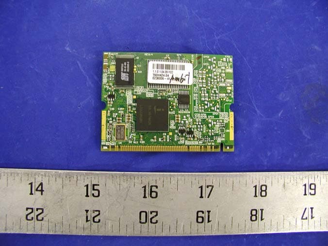
Click to zoom
Application Details
- Equipment Class
- DTS - Digital Transmission System
- Date of Grant
- Mar 19, 2003
- Application Purpose
- Original Equipment
- Date of Application
- Mar 19, 2003
- Equipment Note
- Laptop PC with Wireless LAN Card
- Frequency Range
- 2412.00000000 - 2462.00000000
- Country
- Taiwan
Documents & Files
Document Text
Text extracted from the exhibit documents filed with the FCC. Open a document above to read the original.
Users Manual
1 Ambit Microsystems Corporation U S E R ’ S M A N U A L Model Name T60H424 Ambit Microsystems Corporation 5F-1, 5 Hsin-An Rd., Hsinchu Science-Based Industrial Park, Hsinchu, Taiwan, R.O.C. TEL: 886-3-5784975, FAX: 886-3-5799178 Website: http://www.ambit.com.tw/ 2 Ambit Microsystems Corporation Contents Chapter 1 About the T60H424 MiniPCI Card 1-1 Features 1-2 Applications 1-3 Product Kit Chapter 2 Network Configuration and Planning 2-1 Network Topology 2-2 Roaming Chapter 3 Adapter Installation and Configuration – Windows ® 98 / NT / 2000 3-1 System Requirements 3-2 Inserting the Adapter 3-3.1 T60H424 Driver Installation - Windows ® 98 3-3.2 Adapter Configuration - Windows ® 98 3-3.3 Protocol Installation - Windows ® 98 3-4 T60H424 Setup for Windows ® 2000 Chapter 4 Installing and Navigating the PRISM Configuration Utility 4-1 LAN-Express Configuration Utility - Installation 4-2 LAN-Express Configuration Utility - Navigation Appendix A Troubleshooting Appendix B Glossary 3 Ambit Microsystems Corporation Chapter 1 About the T60H424 MiniPCI Card The IEEE 802.11 T60H424 MiniPCI Card is compatible with any standard, notebook computer Type II or Type III PCMCIA slot / Type III MiniPCI slot. As a Plug-and-Play device, Windows 95/98/2000 will automatically recognize the T60L198 PCMCIA and initiate the installation process. Upon successful installation, the T60H424 MiniPCI card will communicate seamlessly with other T60H424 wireless home and office networking products. 1-1 FEATURES 1. Supports up to 11 Mbps data rate: T-1 line alternative/replacement that dramatically cuts costs. 2. Working range up to 800 ft. in an open environment enhances mobility. 3. Supports point-to-point and point-to-multipoint access provides increased flexibility. 4. Seamless connectivity to wired Ethernet and PC network LAN’s offers quick, trouble-free integration with existing networks. 5. Robust Direct Sequence Spread Spectrum (DSSS) technology provides secure, interference-resistant wireless connection. 6. Wireless connections eliminate the hassle and cost of cabling. 7. Supports a wide range of LAN (Local Area Network) Network Operating Systems (NOS) including Windows ® 98 and Windows ® 2000 8. Easy Plug and Play installation(T60L198). 9. Omni - directional antenna included 10. Greater flexibility to locate or move networked PC’s 1-2 APPLICATIONS T60H424 products offer a fast, reliable, cost-effective solution for wireless client access to the network the following applications and environments: Remote access to corporate network information E-mail, file transfer and terminal emulation Difficult-to-wire environments Historic or older buildings Buildings with asbestos insulation Open areas where wiring is difficult to employ Frequently changing environments Retailers, manufacturers or other organizations that frequently rearrange the workplace or relocate Temporary LANs for special projects or peak time usage Trade shows, exhibitions and construction sites that employ temporary networks. 4 Ambit Microsystems Corporation Retailers, airline and shipping companies that need additional workstations for a peak period and Auditors that require workgroups at customer sites. Access to database for mobile workers Medical, Technical and Retail specialists that require roaming access to a database or other network resources. SOHO (Small Office and Home Office) users Perfect for users that need a small, easy-to-install network that deploys rapidly. Inter-building connection Wireless building-to-building networks are quickly and easily installed, require no monthlylease fees, and provide the flexibility to reconfigure easily. 1-3 PRODUCT KIT The T60H424 product kit includes the following items. Ensure that the items in the following list have been included. If any of the listed items are missing, please contact your local dealer. 1 X T60L198 PCMCIA Type II Adapter or Type III T60H424 MiniPCI Adapter 1 X Driver 1 X User Manual & Utility Chapter 2 Network Configuring and Planning The T60H424 supports legacy Ethernet LAN network configuration options as defined by the IEEE 802.11 standards committee. The T60H424 can be configured as: . Ad-Hoc for departmental or SOHO LANs. . Infrastucture for enterprise LANs. . LAN-Interconnection for to point-to-point link as a campus backbone. 2-1 Network Topology 5 Ambit Microsystems Corporation Ad-Hoc Wireless LAN Notebook with T60L198/T60L244 Notebook with T60L198/T60L244 Desktop PC with T60L198/T60L244 Desktop PC with T60L198/T60L244 Fig.1 Ad-Hoc Wireless LAN An Ad-Hoc wireless LAN is a group of computers. Each equipped with on T60H424 adapter, connected as an independent wireless LAN.Computers in a specific Ad-Hoc wireless LAN must be configured to share the same radio channel. Ad-Hoc wireless LAN configurations are appropriate for branch level departments or SOHO operations. 乙太網路 File Server Desktop PC Desktop PC Desktop PC with T60L198/T60L244 Desktop PC with T60L198/T60L244 Access PointAccess Point Notebook with T60L198/T60L244 Notebook with T60L198/T60L244 Fig.2 Infrastructure Wireless LAN Configuration Desktop PC with T60L198/T60L244 Desktop PC with T60L198/T60L244 The T60H424 provides access to a wired LAN for wireless workstations.An integrated wireless and wired LAN is called an Infrastructure configuration. A group of T60H424 PC users and an Access Point compose a Basic Service Set (BSS).Each T60H424 can talk to any computer in the wired LAN infrastructure via the Access Point. An Infrastructure configuration extends the accessibility of a T60H424 equipped PC to a wired LAN and doubles the effective 6 Ambit Microsystems Corporation wireless transmission range for 2 T60H424 PCs. Since the Access Point is able to forward data within its BSS, the effective transmission range in an infrastucture LAN is doubled. Ad-Hoc Infrastructure Access Point Notebook with T60L198/T60L244 Notebook with T60L198/T60L244 Notebook with T60L198/T60L244 Notebook with…
Text truncated - open the document above for the full version.
Block Diagram
Block diagram description of ISL37400M MiniPCI WLAN Card Receiver path The 2.4GHz RF signal enters via antenna (1) and band pass filter (2) the RF/IF converter ISL3685IR (3) to be converted to 374MHz IF. The 374MHz IF signal then goes through a band pass saw filter (4) to the IQ demodulator ISL3783 (5) to be amplified and IQ demodulated. The demodulated signal goes to the MAC controller / Base Band Processor ISL3874 (6) where the IQ signals are converted into data bits. The data bits are processed by the MAC controller on IEEE 802.11b HR protocol level. This MAC controller is equipped with an SRAM and Flash Memory (7) and also controls the MiniPCI interface (8) with the host. Transmitter Path Data packets coming from the MiniPCI interface (8) are processed by the MAC controller ISL3874 (6) on IEEE 802.11b HR protocol level. The Base band processor then spreads and IQ modulates the signal, which is then converted to 374MHz IF by ISL3783 (5). This 374MHz IF signal is filtered by band pass filter (4) and then converted to 2.4 GHz RF signal by RF/IF converter ISL3685IR (3). The 2.4GHz RF signal is then filtered by Band pass filter (9) and amplified by RF Power Amplifier ISL3984 (10) and finally emitted via the TX antenna (1).
External Photos
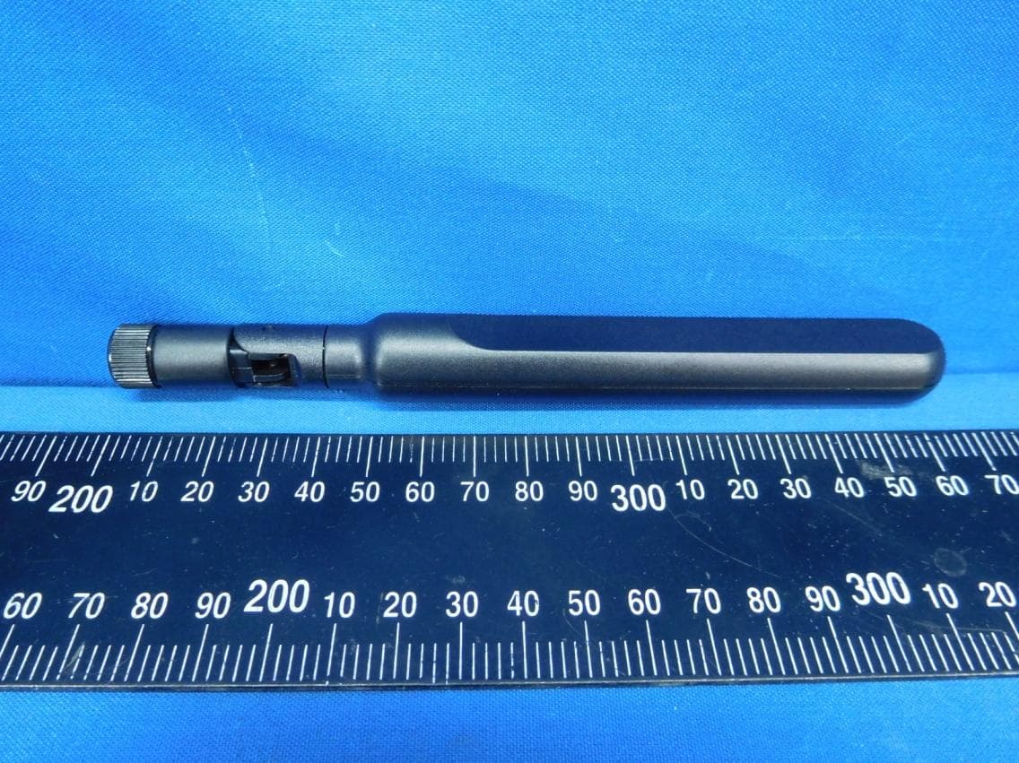
EXHIBIT C - EUT EXTERNAL PHOTOGRAPHS EUT – Top Side View EUT – Top Side View Without Shield EUT – Bottom Side View Antenna View Power Supply
ID Label/Location Info
EXHIBIT A - FCC ID LABEL INFORMATION Proposed FCC ID Label 2.1875”L x 1.0”W Proposed Label Location Rear Side of Laptop / Label Location FCC ID: MCL-T60H42400 This device complies with Part 15 of the FCC Rules. Operation is subject to the following two conditions: (1) this device may not cause harmful interference, and (2) this device must accept any interference received, including interference that may cause undesired operation.
Internal Photos
EXHIBIT C - EUT INTERNAL PHOTOGRAPHS EUT – Top Side View EUT – Top Side View Without Shield EUT – Bottom Side View Module Location within the Notebook 1 Module Location within the Notebook 2 Antenna within the Notebook 1 Antenna within the Notebook 2 Antenna Within the Notebook 3 Antenna Within the Notebook 4
Operational Description
1 TM AN9633 Processing Gain for Direct Sequence Spread Spectrum Communication Systems and PRISM® Introduction This application note addresses the concept of processing gain (PG) of Direct Sequence Spread Spectrum (DSSS) systems. The PRISM chipset is used to implement DSSS radio designs. The processing gain provides the unique properties to the DSSS waveform primarily in terms of interference tolerance. The PG of a DSSS system is centered around the utilization of random codes which are used in conjunction with the data. These random codes are referred as Pseudo Noise (PN) codes. The HSP3824 provides this coding capability for the PRISM. Description In a DSSS system random binary data with a bit rate of r b bits per sec (bps) is multiplied (Exclusive Ored) by a pseudorandom binary waveform, which is at much higher rate and it provides the frequency spreading operation. This pseudorandom (PN) binary source outputs symbols called chips at a constant chip rate r C chips per sec (cps). This is a random, noise like signal and hence the name PN signal. The chip rate is always higher than the bit rate, and the ratio of the chip rate to the bit rate is defined as the processing gain (PG) [3]. The PG is a true signal to jammer (interference) ratio at the receiver after the despreading operation (removal of PN). The rate of the PN code is the one that defines the bandwidth of the transmitted spread waveform. The receiver of a DSSS system must remove the spreading as the first step in the demodulation process. During the despreading operation the receiver must generate a phase locked exact replica of the pseudorandom spreading waveform to match the transmitted signal. This is achieved by the code acquisition, and code tracking loops embedded in the HSP3824. The receiver PN sequence must be exactly in phase with the transmitted PN sequence, and this is achieved by correlation techniques. DSSS Transceiver A DSSS transmitter is shown in Figure 1. The data is denoted by d(t), the spreading signal is denoted by c(t), and the spread waveform q(t) is fed to the BPSK modulator operating at a carrier frequency f C , and the transmitted signal is denoted by x(t). A text book conceptual block diagram of a DSSS receiver is depicted in Figure 2. Note that PRISM is architected to perform the despreading function at baseband (HSP3824) rather than at RF as shown on Figure 2. This example is used for illustration of the concept and not to reflect the actual PRISM implementation. The received signal for this text book example is the combination of the transmitted spread spectrum signal and a narrow band jammer x J (t). The locally generated despreading sequence is denoted by c’(t), and should be equal to c(t). The despread signal is then band pass filtered before data demodulation and d’(t) should be equal to d(t). PG Benefits The primary benefit of processing gain is its contribution towards jamming resistance to the DSSS signal. The PN code spreads the transmitted signal in bandwidth and it makes it less susceptible to narrowband interference within the spread BW. The receiver of a DSSS system can be viewed as unspreading the intended signal and at the same time spreading the interfering waveform. This operation is best illustrated on Figure 3. Figure 3 depicts the power spectral density (psd) functions of the signals at the receiver input, the despread signal, the bandpass filter power transfer function, and the band pass filter output. Figure 3 graphically describes the effect of the processing gain on a jammer. The jammer is narrow, and has a highly peaked psd, while the psd of the DSSS is wide and low. The despreading operation spreads the jammer power psd and lowers its peak, and the BPF output shows the effect on the signal to jammer ratio. FIGURE 16. DSSS TRANSMITTER d(t) q(t) c(t) x(t) COS(ω O t) CODE GENERATOR FIGURE 17. DSSS RECEIVER d’(t)y(t) c’(t) x(t) + x j (t) COS(ω O t) PN GENERATOR BPF H(f) x’(t) LPF Application NoteAugust 1996 Authors: John Fakatselis Title N96 ) ub- t o- s- in rect quen read ec- m m- ni- ion s- ms d IS utho ey- rds ter- rpo- ion, mi- n- ctor, IS re- s m- CAUTION: These devices are sensitive to electrostatic discharge; follow proper IC Handling Procedures. 1-888-INTERSIL or 321-724-7143 |Intersil (and design) is a trademark of Intersil Americas Inc. Copyright © Intersil Americas Inc. 2001. All Rights Reserved PRISM® is a registered trademark of Intersil Americas Inc. PRISM and design is a trademark of Intersil Americas Inc. 2 If for example, BPSK modulation is used and an Eb/No of lets say 14dB is required to achieve a certain BER performance, when this waveform is spread with a processing gain of 10dB then the receiver can still achieve its required performance with the signal having a 4dB power advantage over the interference. This is derived from the 14dB required minus the 10dB of PG. The higher the processing gain of the DSSS waveform the more the resistance to interference of the DSSS signal. The classical definition of processing gain is the 10 Log number [r C /r B ] in dB. By this definition a system that has a data rate of 1MBPS and a chip rate (rate of PN code) of 1MCPS will have a PG of 10.41dB. Using the PRISM chip set each data bit is x-ored with an 11 bit sequence for this particular example. The processing gain can be then viewed as the 10Log[11]dB where 11 is the length of the PN code. If a code with a length of 16 bits is to be used then the processing gain is equivalent to 10 Log[16] dB or 12.04dB. To this end these PN signals must posses certain mathematical properties to be useful as part of a DSSS system. Primarily the PN codes that are useful must have very good autocorrelation and crosscorrelation properties as well as maintaining some randomness properties. The DSSS receiver is utilizing a reference PN sequence which is a replica to the transmitted sequence and when it detects correlation between the reference and the incoming sequences it declares initial a…
Text truncated - open the document above for the full version.
Schematics
1 2 3 4 5 6 78 ABCD 8 7 6 5 4 3 2 1 D CBA AMBIT Version PAGE of Title Checked Prepared Approved 0 4 1 SCHEMAICT60H424James Huang DOC 1 PEMONO_PHONERESET#ID0#SDATA_OUTSYNCSDATA_INBIT_CLK+M3.3VMPCIACTLREQ#CLKC/BE3#C/BE2#IRDY#SERR#PERR#C/BE1#CLKRUN#LED1PA_PELED1_GRNNLINT#LPME#LGNT#RST#PARFRAME#TRDY#STOP#DEVSEL#C/BE0#LIDSELAD(0..31)AD(0..31)VCCS+3.3VVCCAVCCB44MHZ_REF44MHZ_CWRADIO_PE MINI_PCIMINI_PCI.sch 44MHZ_REFTXQ+TXQ-TXI+TXI-RXQ+RXQ-RXI+RXI-VREFRX_IF_AGCRX_RF_AGCTX_IF_AGCIF_DETTX_DETANTSELANTSEL*LE_IFT/R SWT/R SW*CAL_ENLE_RFPA_PEPE1RADIO_PESCLK_RF_IFSD_RF_IFPE2MPCIACTLED1_GRNNLPME#LIDSELPARFRAME#TRDY#STOP#DEVSEL#C/BE0#C/BE1#C/BE2#C/BE3#PERR#SERR#LREQ#RST#LINT#IRDY#LGNT#CLKLED1MD(0..15)MD(0..15)MA(1..17)MA(0..17)MD(0..31)MA(1..17) WLAN1WLAN1.SCH TXQ-TXQ+VREFTXI-TXI+RXQ-RXQ+RXI+RXI-PE+3.3VTX_DETTX_IF_AGCRX_IF_AGCIF_DETPE1PE2CAL_EN44MHZ_CWLE_RFSCLK_RF_IFSD_RF_IFLE_IFT/R SWT/R SW*ANTSELANTSEL*RX_RF_AGCVCCAVCCBPE1PE2AGND WLAN2WLAN2.Sch 1 2 3 4 5 6 78 ABCD 8 7 6 5 4 3 2 1 D CBA AMBIT Version PAGE of Title Checked Prepared Approved 0 4 2 SCHEMAICT60H424James Huang DOC RING 2 8PMJ-1 4 8PMJ-2 6 8PMJ-4 8 8PMJ-5 10 LED2_YELP 12 LED2_YELN 14 RESERVED 16 5V 18 RESERVED 22 RST# 26 GNT# 30 GND 32 PME# 34 RESERVED 36 3.3V 40 AD[28] 42 AD[24] 46 IDSEL 48 AD[22] 52 AD[20] 54 PAR 56 AD[18] 58 AD[16] 60 GND 62 FRAME# 64 TRDY# 66 STOP# 68 3.3V 70 DEVSEL# 72 GND 74 AD[15] 76 AD[13] 78 AD[11] 80 C/BE[0]# 86 GND 102 AC_CODEC_IDO# 108 SYS_AUDIO_IN GND 118 INTA# 20 3.3VAUX 24 3.3V 28 AD[30] 38 AD[26] 44 GND 50 GND 82 AD[09] 84 3.3V 88 AD[06] 90 AD[04] 92 AD[02] 94 RESERVED 100 M66EN 104 AC_SDATA_OUT 106 AC_RESET# 110 RESERVED 112 GND 114 SYS_AUDIO_IN 116 AUDIO_GND 120 AD[00] 96 RESERVED 98 MPCIACT# 122 3.3VAUX 124 TIP 1 8PMJ-3 3 8PMJ-6 5 8PMJ-7 7 8PMJ-8 9 LED1_GRNP 11 LED1_GRNN 13 CHSGND 15 INTB# 17 3.3V 19 RESERVED 21 GND 23 CLK 25 GND 27 REQ# 29 AD[31] 33 GND 37 IRDY# 61 +3.3V 63 CLKRUN# 65 SERR# 67 GND 69 PERR# 71 AD[03] 95 SYS_AUDIO_OUT 115 3.3V 31 AD[29] 35 AD[27] 39 AD[25] 41 RESERVED 43 C/BE[3]# 45 AD[23] 47 GND 49 AD[21] 51 AD[19] 53 GND 55 AD[17] 57 C/BE[2]# 59 C/BE[1]# 73 AD[14] 75 GND 77 AD[12] 79 AD[10] 81 GND 83 AD[08] 85 AD[07] 87 +3.3V 89 AD[05] 91 RESERVED 93 5V 97 MOD_AUDIO_MON 111 AUDIO_GND 113 SYS_AUDIO_OUT GND 117 AD[01] 99 GND 101 AC_SYNC 103 AC_SDATA_IN 105 AC_BIT_CLK 107 AC_CODEC_ID1# 109 AUDIO_GND 119 RESERVED 121 VCC5VA 123 P1MINIPCI SOLDER SIDE AD1AD3AD5AD7AD8AD10AD12AD14AD17AD19AD21AD23AD25AD27AD29AD31 AD0AD2AD4AD6AD9AD11AD13AD15AD16AD18AD20AD22AD24AD26AD28AD30 RST#FRAME#TRDY#STOP#DEVSEL# PERR#C/BE1#IRDY#C/BE2#CLKRUN#SERR#C/BE3# PAR LED1 R223 R/47/0402/5% CLK 12 C81C/104K/16V/X7R/0603 12 C31C/104K/16V/X7R/0603 12 C9C/104K/16V/X7R/0603 1 2 L17 B/BLM21P300S 1 2 L3 B/BLM21P300S 12 R5R/0/0402/5% +3.3V R225R/0/0402/5% LINT# 1 2 R702 R/0/0402/5% INTA# LGNT# LREQ# LPME# C/BE0# V1 MONO_PHONE RESET# ID0# SDATA_OUT SYNC SDATA_IN BIT_CLK 12 C730C/10U/6.3V/M/A 3.3VAUX 12 C717C/104K/16V/X7R/0603 +M3.3V +M3.3V 1 2 R740R/0/5%/1206 LIDSEL 1 2 R102 NI R/0/0402/5% 12 R8 NI R/10K/0402/5% VCCS 1 2 R12 NI R/0/0402/5% 1 2 R13NI R/0/0402/5% R14 NI R/10K/0402/5% MPCIACT MPCIACT MONO_PHONERESET#ID0#SDATA_OUT LREQ#CLKC/BE3#C/BE2#IRDY#SERR#PERR#C/BE1#CLKRUN# LED1 LINT# LPME# LGNT# RST# PAR FRAME# TRDY# STOP# DEVSEL# C/BE0# LIDSEL AD(0..31) AD(0..31) SYNCSDATA_INBIT_CLK 2 12 C40 C/104K/16V/X7R/0603 12 C41 C/104K/16V/X7R/0603 12 C42 C/104K/16V/X7R/0603 VCCA +3.3V FAA 2.8V IN 1 SHDN 3 BP 4 GND 2 OUT 5 U7RT9167-28CB 12 C135 C/104K/16V/X7R/0603 12 C133 C/104K/16V/X7R/0603 12 C137 C/104K/16V/X7R/0603 VCCB +3.3V 2.8V IN 1 SHDN 3 BP 4 GND 2 OUT 5 U15RT9167-28CB RADIO_PE 12 3 147 U22A U/7S08/TSSOP14 FAA VCCS 1 2 R224 NI R/0/0402/5% RADIO_PE PA_PE 45 6 U22B U/7S08/TSSOP14 1 2 R226 NI R/0/0402/5% FAA PA_PE PE 12 R24 R/0/0402/5% 1 2 R15 R/1.5K/0402/1% 12 L1 L/0.56UH/1008 1 2 C33 C/104K/16V/X7R/0603 12 R82 R/0/0402/5% 1 2 C27 C/102K/50V/X7R/0402 12 C24 C/220J/50V/COG/0402 VDD 4 ENB 1 GND 2 OUT 3 U6U/OSC/44MHz 12 L21B/BLM21P300S 44MHZ_CW44MHZ_REF +3.3V 12 C141 NI C/680J/50V/COG/0402 44MHZ_REF 44MHZ_CW FAA R230 NI R/0/0402/5% R231R/10K/0402/5% VCCS FAA R7 NI R/0/0402/5% LED1_N R232 R/0/0402/5% RA1 NI R/0/0603/5% RA2 R/0/0603/5% T60H418.00T60H424.00 12 C134 C/475Z/16V/Y5V/1206 12 C102 C/475Z/16V/Y5V/1206 12 C14 C/475Z/16V/Y5V/1206 12 C34 C/475Z/16V/Y5V/1206 12 C43 C/475Z/16V/Y5V/1206 12 C38 C/475Z/16V/Y5V/1206 12 C136 C/475Z/16V/Y5V/1206 3.3VAUX 3.3VAUX TR1E 1 TR2C 3 TR2E 4 TR1C 6 TR2B 5 TR1B 2 U80NI UMZ1N 1 2 R6NI R/1.1K/0402/5% 12 C84 NI C/106M/6.3V/X5R/0805 1 2 R9 NI R/10K/0402/5% 12 R85NI R/1.1K/0402/1% 1 2 R84 NI R/10K/0402/5% PA_PE 1 2 R95R/0/0402/5% 1 2 R96NI/R/0/0402/5% LED1_GRNN 1 2 R81 NI R/1.1K/0402/1% VCCS LED1_N LED2_OUT VCCS 1 2 3 4 5 6 78 ABCD 8 7 6 5 4 3 2 1 D CBA AMBIT Version PAGE of Title Checked Prepared Approved 0 4 3 SCHEMAICT60H424James Huang DOC PL4-MA19 A4 MA18 A3 MA17 B4 MA16 C3 MA15 B3 MA14 A1 MA13 C2 MA12 E3 MA11 B1 MA10 D2 MA9 D3 MA8 C1 MA7 F4 MA6 E2 MA5 D1 MA4 F2 MA3 E1 MA2 F3 MA1 F1 MA0/MWEH- G2 MD14 G1 MD0 P2 MD1 R1 MD2 P3 MD3 N2 MD4 P1 MD5 N3 MD6 N1 MD7 M2 MD8 M3 MD9 M1 MD10 J3 MD11 H1 MD12 H2 MD13 H3 MD15 H4 MLBE L3 MOE L1 MWE/MWEL L2 RAMCS K2 NVCS K1 PJ4 T2 VRFE P11 IRFE N12 HAD31 A8 HAD30 A9 HAD29 C8 HAD28 A10 HAD27 B9 HAD26 B10 HAD25 C9 HAD24 A11 HAD23 B11 HAD22 B12 HAD21 A12 HAD20 A13 HAD19 C12 HAD18 A14 HAD17 C13 HAD16 C14 HAD15 E14 HAD14 E15 HAD13 F16 HAD12 F15 HAD11 F14 HAD10 G16 HAD9 G15 HAD8 G14 HAD7 H15 HAD6 G13 HAD5 J15 HAD4 J14 HAD3 K14 HAD2 K15 HAD1 L14 HAD0 L16 HBE3 C10 HBE2 B14 HBE1 E16 HBE0 H16 HINTA C6 HRESET D6 HFRAME B15 HIRDY A15 HTRDY A16 HREQ B7 HSERR B16 HSTOP C16 HDEVSEL D15 HPERR D16 HGNT C7 HPCLK A7 HPAR B13 HIDSEL C11 HPME B8 PJ0 P5 PJ1 T1 PJ2 R3 VDD P6 VDD D4 VDD D7 VDD D9 VDD D11 VDD D14 VDD F13 VDD H13 VDD K16 VDD M15 VDD N5 VDD N4 VDD K4 VDD G3 VDD E4 VDDA M13 VDDA P12 VDDA R11 VDDA T8 VDDA R8 VDDA P9 PJ5 T4 PJ6 P4 PJ7 T3 PK0 R5 PK1 R4 PK2 N7 PK3 R6 PK4 T5 PK7 P7 PL3 P8 PL7 T6 RX_IF_AGC T16 RX_RF_AGC P16 RX_IF_DET R10 RXI+ R7 RXI- T7 RXQ+ R9 RXQ- T9 TX_AGC_IN T10 TX…
Text truncated - open the document above for the full version.
Test Report
Note: This test report is specially limited to the above client company and the product model only. It may not be duplicated without prior written consent of Bay Area Compliance Laboratory Corporation. This report must not be used by the client to claim product endorsement by NVLAP or any agency of the U.S. Government. FCC PART 15 SUBPART C EMI MEASUREMENT AND TEST REPORT For AMBIT Microsystems Corporation 4-1, Ming Shen Street, Tu Chen Industrial District. Tu Chen, Taipei Hsien 236, Taiwan, R.O.C. FCC ID: MCL-T60H42400 March 13, 2003 This Report Concerns: Original Report Equipment Type: MiniPCI IIIB Wireless LAN Card Test Engineer: Jerry Wang Report No.: R0302123 Test Date: February 27, 2003 Reviewed By: Hans Mellberg Prepared By: Bay Area Compliance Laboratory Corporation 230 Commercial Street Sunnyvale, CA 94085 Tel: (408) 732-9162 Fax: (408) 732 9164 AMBIT Microsystems Corporation FCC ID: MCL-T60H42400 Report # R0302123Rpt.doc FCC 15 Subpart C Test Report Page 2 of 36 TABLE OF CONTENTS 1 - GENERAL INFORMATION..................................................................................................................................4 1.1 PRODUCT DESCRIPTION FOR EQUIPMENT UNDER TEST (EUT) ..............................................................................4 1.2 OBJECTIVE.............................................................................................................................................................4 1.3 RELATED SUBMITTAL(S)/GRANT(S).......................................................................................................................4 1.4 TEST METHODOLOGY............................................................................................................................................4 1.5 TEST FACILITY.......................................................................................................................................................5 1.6 TEST EQUIPMENT LIST AND DETAILS.....................................................................................................................5 1.7 HOST SYSTEM CONFIGURATION LIST AND DETAILS..............................................................................................6 1.8 LOCAL SUPPORT EQUIPMENT LIST AND DETAILS...................................................................................................6 2 - SYSTEM TEST CONFIGURATION.....................................................................................................................7 2.1 JUSTIFICATION.......................................................................................................................................................7 2.2 EUT EXERCISE SOFTWARE....................................................................................................................................7 2.3 SPECIAL ACCESSORIES...........................................................................................................................................7 2.4 SCHEMATICS / BLOCK DIAGRAM...........................................................................................................................7 2.5 EQUIPMENT MODIFICATIONS.................................................................................................................................7 2.6 CONFIGURATION OF TEST SYSTEM.........................................................................................................................8 2.7 TEST SETUP BLOCK DIAGRAM...............................................................................................................................8 3 - SUMMARY OF TEST RESULTS..........................................................................................................................9 4 - PEAK OUTPUT POWER MEASUREMENT ....................................................................................................10 4.1 STANDARD APPLICABLE......................................................................................................................................10 4.2 MEASUREMENT PROCEDURE................................................................................................................................10 4.3 MEASUREMENT RESULT......................................................................................................................................10 5 - SPURIOUS EMISSION.........................................................................................................................................13 5.1 STANDARD APPLICABLE......................................................................................................................................13 5.2 MEASUREMENT PROCEDURE................................................................................................................................13 5.3 MEASUREMENT DATA..........................................................................................................................................13 6 - PEAK POWER SPECTRAL DENSITY ..............................................................................................................17 6.1 STANDARD APPLICABLE......................................................................................................................................17 6.2 MEASUREMENT PROCEDURE................................................................................................................................17 6.3 TEST RESULTS.....................................................................................................................................................17 7 - 6 DB BANDWIDTH...............................................................................................................................................20 7.1 STANDARD APPLICABLE...........................................................................................................................…
Text truncated - open the document above for the full version.
Test Setup Photos
EXHIBIT B - TEST SETUP PHOTOGRAPHS Conducted Emission Radiated Emission
Contact Information
Applicant
Mrs. Rio Chen(Compliance Deputy Manager)
Test Firm
Bay Area Compliance LaboratoryJohn Chan
Technical Specifications
| # | Rule Parts | Frequency Range | Power Output |
|---|---|---|---|
| 1 | 15C | 2.41 GHz - 2.46 GHz | 41.88 mW |
Other Applications from HON HAI Precision Ind. Co., Ltd.
MCLT77W968
Jun 03, 2021LTE M.2 Module
Equipment Class
CBE - Citizens Band End User Devices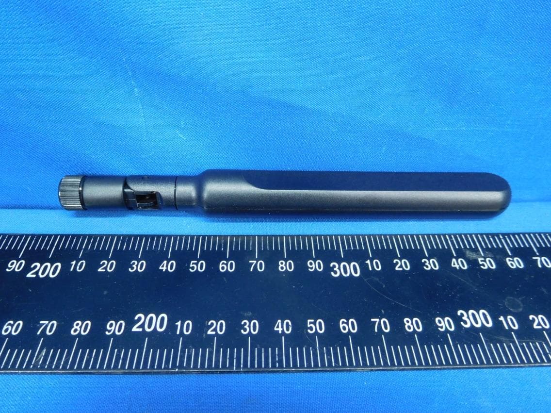
MCLT77W968C9
Feb 13, 2020LTE M.2 Module
Equipment Class
PCB - PCS Licensed Transmitter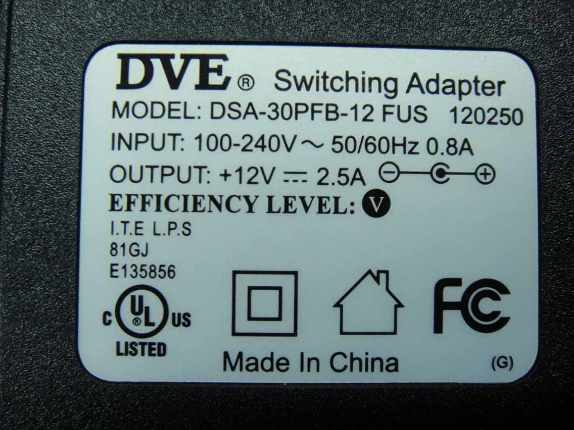
MCLADB1761WF
Jun 03, 2015IP Set-Top Box with Wi-Fi 11ac
Equipment Class
DTS - Digital Transmission System
MCLADB1761W
Jun 02, 2015IP Set-Top Box
Equipment Class
DTS - Digital Transmission System
MCLT77H566
Feb 16, 2015WiFi/BT Module
Equipment Class
DTS - Digital Transmission System