MKDAR147MOBILE TRANSCEIVER
ADI Communications Corporation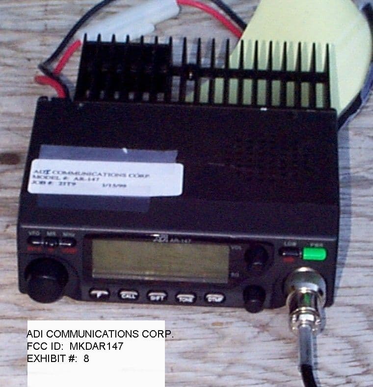
Click to zoom
Application Details
- Equipment Class
- CSR - Scanning Receiver
- Date of Grant
- May 10, 1999
- Application Purpose
- Original Equipment
- Date of Application
- Mar 16, 1999
- Equipment Note
- MOBILE TRANSCEIVER
- Frequency Range
- 130.00000000 - 179.99500000
- Country
- Taiwan
Documents & Files
Document Text
Text extracted from the exhibit documents filed with the FCC. Open a document above to read the original.
Cover Letter(s)
TIMCO ENGINEERING INC. 849 NW STATE ROAD 45 PO BOX 370 NEWBERRY, FLORIDA 32669 888-472-2424 OR 352-472-5500 FAX 352-472-2030 email:[email protected] 6 MAY 1999 TO: MR. GREGORY CZUMAK FROM: SID SANDERS Federal Communications Commission Office of Science & Technology 7435 Oakland Mills Road Columbia, MD 21046 FAX #: 1-301-344-2050 SUBJECT: FCCID: MKDAR147 REFERENCE: CONFIRMATION #EA93544 1. ATTACHED IS A DRAFT OF THE THEORY OF OPERATION. 2. THE TUNING RANGE OF THE RECEIVER IS 132-179MHz AND THE TRANS- MITTER IS 144-148MHz FOR THIS AMATEUR TRANSCEIVER. 3. TO THE BEST OF MY KNOWLEDGE AN AMATEUR TRANSMITTER DOES NOT REQUIRE ANY APPROVALS. 4. ATTACHED YOU WILL FIND ADDITIONAL MEASUREMENTS ON THE RECEIVER AT THE BAND EDGES. IF YOU HAVE ANY OTHER QUESTIONS PLEASE LET ME KNOW. REGARDS, SID SANDERS F:\FCC\FCCINQ\GC90506.FAX
Operational Description
DRAFT DRAFT DESCRIPTION OF FREQUENCY DETERMINING AND STABILING CIRCUIT 2.1 INTRODUCTION The frequencies for transmitter and receiver local frequencies are all drived from a single 4.0 (MHz) crystal by means of a CPU, U203. The first local oscillator frequency is 10.7MHz below the incoming frequency. The CPU generates the fundamental frequency and controls the VCO, Q1502& Q1501. During transmit, the VCO of the PLL can only operate 144.000 MHz to 148.000MHz. The VCO operating frequency for the receiver is 121.300MHz to 168.300MHz at the as the first local oscillator, injected through the buffer AMP Q13 into the first TR Mixer Q4. 2.2 DESCRIPTIONS OF EACH BLOCK (1) INTRODUCTION The synthesizer is implemented with the following components: PLL IC U203, Q1501 & Q1502 VCO, VARICAP Diode D9 The CPU U203 is a CMOS LSI that includes prescaller, the U204, U206, U207, U208 Varicap. Transistor Q10 is clapp oscillator circuit to operate as part of the VCO. The Q28/Q29 are switch transistor to connect or disconnect the tuning capacitor in the VCO oscillator tank circuit for transmitter or receiver. The Q13 works as a buffer AMP for RX local frequencies and TX carrier generating frequencies. (2) REFERENCE FREQUENCY The 4.0MHz Crystal, make a reference frequency oscillator with internal amplifier. (3) VCO The Q1501 & Q1502 and surrounding parts are consisting a clapp oscillator works a VCO of U4 & U203 with appropriate control voltage on D301. The VCO can be oscillate over the required range of 121.3MHz to 168.3MHz. (4) PROGRAMMABLE DIVIDER AND ITS CONTROL The programmable inputs for each channels are setted IC inside. Each input signal to control the CPU is done with the provided AAR-147 DTMF BOARD. Key Matrix input pins – PIN25 to PIN28 and for each key matrix input, an internal code convert EPROM provides the appropriate binary control to the u1 & u2, U3 for that channel. Since the binary number necessary to change during transmit and receive, an additional bit is required at CPU to allow the ROM to recognizing the status is TX or RX. During transmit, the push to talk switch makes PIN.42 of CPU IC is hi digitally under transmit mode. The programmable divider to PLL. The output is fed to the phase detector for comparing with the reference frequency inside. (5) PHASE DETECTOR AND VCO CONTROL The phase detector is a digital phase comparator which compares the phase of the reference signal with programmable divider output square waves and develops a series of pulses whose DC level depends on the phase error of each signal. The phase detector pulse output is fed to an active low pass filter, and fed to varicap D9 control the VCO frequency. (6) TRANSMITTER/RECEIVER BUFFER/AMP Output signal of Q1502 is fed into the buffer AMP Q13 to increase the strength of TX carrier frequency and first local frequencies. (7) SWITCHING OF TUNING CAPACITOR IN VCO The VCO circuit must tune with a wide range of frequencies 132-179.00MHz for the receiver and 144.00 to 148.00MHz for the transmitter. To comply above range of VCO, the tuning capacitance should switched for transmission or reception. The tuning circuit consists with Q1402, U1401 q1404, Q1403 & LPF. when the VCO is working as a TX, the voltage is turned off of the receiver (8) RECEIVER LOCAL OSCILLATOR OUTPUTS 1 st MIXER: The output signals of D11 is injected to the sources of 1 st mixer Q4 in the 1 st mixer section. FM signals are recovered with envelope detector. F:\CUS\A\ADI\THEORY OF OPERATION.doc
Test Report
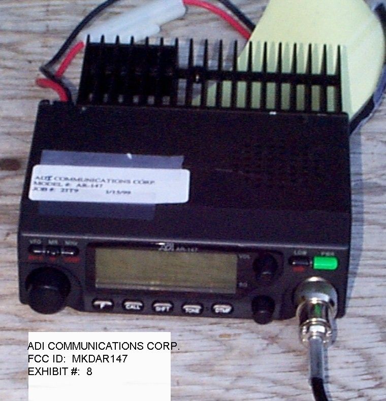
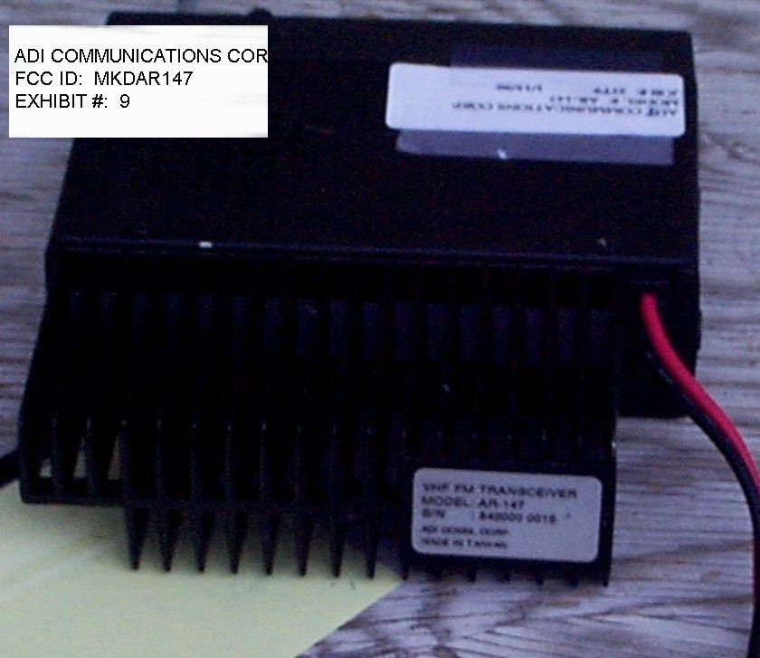
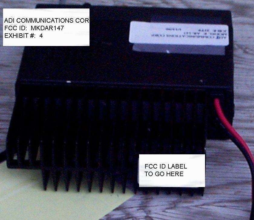
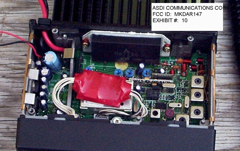
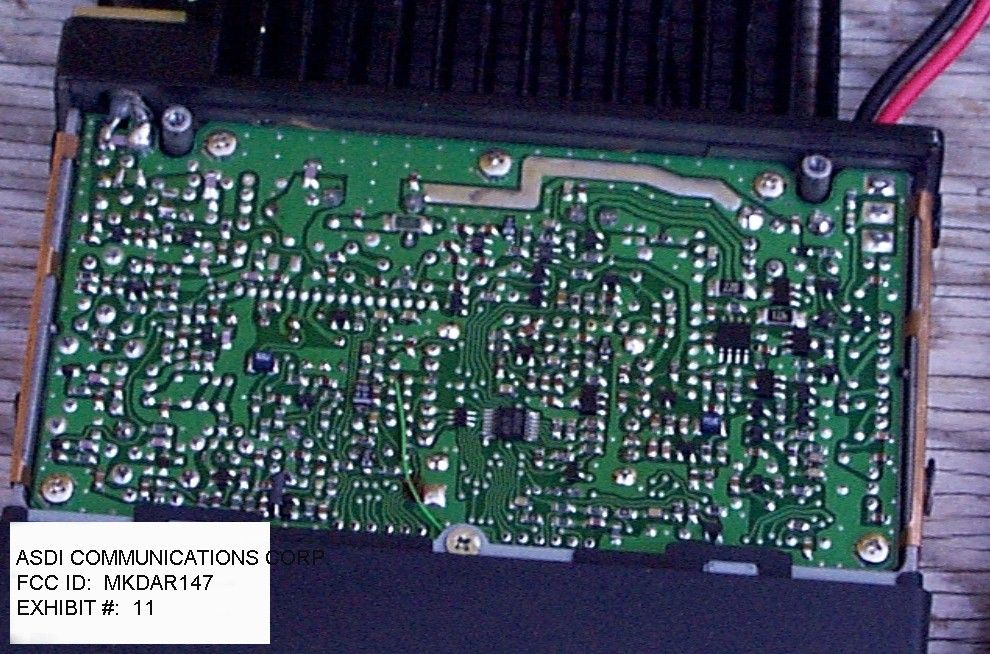
TABLE OF CONTENTS LIST APPLICANT: ADI COMMUNICATIONS CORP. FCC ID: MKDAR147 TEST REPORT CONTAINING: PAGE 1......TEST PROCEDURE PAGE 2......TEST PROCEDURE & CIRCUIT DESCRIPTION PAGE 3......RADIATION INTERFERENCE TEST DATA EXHIBITS CONTAINING: EXHIBIT 1............POWER OF ATTORNEY LETTER EXHIBIT 2............TEST SET UP PHOTO EXHIBIT 3............FCC ID LABEL SAMPLE EXHIBIT 4............SKETCH OF FCC ID LABEL LOCATION EXHIBIT 5............BLOCK DIAGRAM EXHIBIT 6A...........SCHEMATIC - DTMF BOARD EXHIBIT 6B...........SCHEMATIC - A1A1 EXHIBIT 6C...........SCHEMATIC - MIC ASSY. EXHIBIT 6D...........SCHEMATIC - MAIN EXHIBIT 7A-7TT.......INSTRUCTION MANUAL EXHIBIT 8............EXTERNAL FRONT VIEW PHOTOGRAPH EXHIBIT 9............EXTERNAL REAR VIEW PHOTOGRAPH EXHIBIT 10...........INTERNAL COMPONENT SIDE PHOTOGRAPH EXHIBIT 11...........INTERNAL SOLDER SIDE PHOTOGRAPH APPLICANT: ADI COMMUNICATIONS CORP. FCC ID: MKDAR147 REPORT #: F:\CUS\A\ADI\ADI21T9.RPT PAGE: TABLE OF CONTENTS LIST APPLICANT: ADI COMMUNICATIONS CORP. FCC ID: MKDAR147 TEST EQUIPMENT LIST 1. Spectrum Analyzer: Hewlett Packard 8566B - Opt 462, w/ preselector 85685A, & Quasi-Peak Adapter HP 8565OA, & HP 8449B - OPT H02 Cal. 6/26/98 2. Signal Generator, Hewlett Packard 8640B, cal. 10/1/98 3. Eaton Biconnical Antenna Model 94455-1 20-200 MHz Serial No. 0997 Cal. 5/15/98 4. Electro-Metric Dipole Kit, 20-1000 MHz, Model TDA-30 10/15/98 5. Electro-Metric Horn 1-18 GHz, Model RGA-180, Cal. 8/15/98 6. Electro-Metric Antennas Model TDA-30/1-4,Cal. 10/15/98 7. Electro-Metric Line Impedance Stabilization Network Model No. EM-7821, Serial No. 101; 100KHz-30MHz 50uH. Cal.11/19/98 8. Electro-Metric Line Impedance Stabilization Network Model No. EM-7820, Serial No. 2682; 10KHz-30MHz 50uH. Cal. 11/19/98 9. Special low loss cable was used above 1 GHz 10. Tenney Temperature Chamber TEST PROCEDURE GENERAL: This report shall NOT be reproduced except in full without the written approval of TIMCO ENGINEERING, INC. RADIATION INTERFERENCE: The test procedure used was ANSI STANDARD C63.4-1992 using a HEWLETT PACKARD spectrum analyzer with a prese- lector. The bandwidth of the spectrum analyzer was 100 kHz with an appropriate sweep speed. The analyzer was calibrated in dB above a microvolt at the output of the antenna. The resolution bandwidth was 100KHz and the video bandwidth was 300KHz. The ambient temperature of the UUT was 65oF with a humidity of 52%. FORMULA OF CONVERSION FACTORS: The Field Strength at 3m was estab- lished by adding the meter reading of the spectrum analyzer (which is set to read in units of dBuV) to the antenna correction factor sup- plied by the antenna manufacturer. The antenna correction factors are stated in terms of dB. The gain of the Preselector was accounted for in the Spectrum Analyzer Meter Reading. Example: Freq (MHz) METER READING + ACF = FS 33 20 dBuV + 10.36 dB = 30.36 dBuV/m @ 3m POWER LINE CONDUCTED INTERFERENCE: The procedure used was ANSI STAN- DARD C63.4-1992 using a 50uH LISN. Both lines were observed. The bandwidth of the spectrum analyzer was 10kHz with an appro- priate sweep speed. The ambient temperature of the UUT was 80oC with a humidity of 76%. APPLICANT: ADI COMMUNICATIONS CORP. FCC ID: MKDAR147 REPORT #: F:\CUS\A\ADI\ADI21T9.RPT PAGE #: 1 TEST PROCEDURES CONTINUED APPLICANT: ADI COMMUNICATIONS CORP. FCC ID MKDAR147 ANSI STANDARD C63.4-1992 10.1.7 MEASUREMENT PROCEDURES: The unit under test was placed on a table 80 cm high and with dimensions of 1m by 1.5m. The table used for radiated measurements is capable of continuous rotation. When an emission was found, the table was rotated to produce the maximum signal strength. At this point, the antenna was raised and lowered from 1m to 4m. The antenna was placed in both the horizontal and vertical planes. The situation was similar for the conducted measurement except that the table did not rotate. The EUT was setup as described in ANSIC63.4-1992 with the EUT 40 cm from the vertical ground wall. CIRCUIT_DESCRIPTION: In the receive mode the signal comes in on the receive antenna to the low pass filter to the antenna change over switch. Then to a tuned circuit and then to the RF amplifier Q3. From Q3 the signal goes to a bandpass filter to the mixer Q4. The output of the Mixer goes to a 10.7MHz crystal filter then to the IF amplifier Q5 and then to 2nd mixer and IF amplifier intergrated circuit A1A1. The output of the detector drives the audio amplifier U5 which is connected to the speaker. ANTENNA_AND_GROUND_CIRCUITRY This unit makes use of a external 5 inch antenna. The antenna is inductively coupled. This unit is powered from a 9.0V battery. No ground connection is provided. The unit relies on the ground tract of the printed circuit board. APPLICANT: ADI COMMUNICATIONS CORP. FCC ID: MKDAR147 REPORT #: F:\CUS\A\ADI\ADI21T9.RPT PAGE #: 2 APPLICANT: ADI COMMUNICATIONS CORP. FCC ID: MKDAR147 NAME OF TEST: RADIATION INTERFERENCE RULES PART NUMBER: 15.109 REQUIREMENTS: 30 to 80 MHz: 40.0 dBuV/M @ 3 METERS 88 to 216 MHz: 43.5 dBuV/M 216 to 960 MHz: 46.0 dBuV/M ABOVE 960 MHz: 54.0 dBuV/M TEST RESULTS: A search was made of the spectrum from 30 to 1000 MHz and the measurements indicate that the unit DOES meet the FCC requirements. TEST DATA: ANTENNA TUNED EMISSION METER READING COAX CORRECTION FIELD FREQ FREQUENCY AT 3 METERS LOSS FACTOR STRENGTH MARGIN MHz MHz dBuV dB dB dBuV/m@3m dB ANT 144.00 133.34 20.10 0.80 14.44 35.34 8.16 V 144.00 266.68 27.40 1.40 13.86 42.66 3.34 H 144.00 400.02 17.30 1.60 17.00 35.90 10.10 H 144.00 533.36 7.10 1.60 19.57 28.27 17.73 H 146.00 135.32 18.90 0.80 15.17 34.87 8.63 V 146.00 270.64 25.40 1.40 13.97 40.77 5.23 H 146.00 405.96 13.00 1.60 17.14 31.74 14.26 H 146.00 541.28 5.50 1.60 19.63 26.73 19.27 H 148.00 137.32 16.00 0.80 15.91 32.71 10.79 V 148.00 274.64 22.90 1.40 14.09 38.39 7.61 H 148.00 411.96 14.50 1.60 17.28 33.38 12.62 H 148.00 549.28 6.70 1.60 19.69 27.99 18.01 H SAMPLE CALCULATION: FSdBuV/m = MR(dBuV) + ACFdB. TEST PROCEDURE…
Text truncated - open the document above for the full version.
Test Report
APPLICANT: ADI COMMUNICATIONS CORP. FCC ID: MKDAR147 NAME OF TEST: RADIATION INTERFERENCE RULES PART NUMBER: 15.109 REQUIREMENTS: 30 to 80 MHz: 40.0 dBuV/M @ 3 METERS 88 to 216 MHz: 43.5 dBuV/M 216 to 960 MHz: 46.0 dBuV/M ABOVE 960 MHz: 54.0 dBuV/M TEST RESULTS: A search was made of the spectrum from 30 to 1000 MHz and the measurements indicate that the unit DOES meet the FCC requirements. TEST DATA: ANTENNA TUNED EMISSION METER READING COAX CORRECTION FIELD FREQ FREQUENCY AT 3 METERS LOSS FACTOR STRENGTH MARGIN MHz MHz dBuV dB dB dBuV/m@3m dB ANT 132.00 121.38 19.90 0.80 10.01 30.71 12.79 V 132.00 242.76 24.80 1.20 13.17 39.17 6.83 H 132.00 364.14 14.40 1.40 15.96 31.76 14.24 H 144.00 133.34 20.10 0.80 14.44 35.34 8.16 V 144.00 266.68 27.40 1.40 13.86 42.66 3.34 H 144.00 400.02 17.30 1.60 17.00 35.90 10.10 H 144.00 533.36 7.10 1.60 19.57 28.27 17.73 H 148.00 137.32 16.00 0.80 15.91 32.71 10.79 V 148.00 274.64 22.90 1.40 14.09 38.39 7.61 H 148.00 411.96 14.50 1.60 17.28 33.38 12.62 H 148.00 549.28 6.70 1.60 19.69 27.99 18.01 H 179.00 168.37 21.60 0.90 18.27 40.77 2.73 V 179.00 336.74 13.80 1.40 15.17 30.37 15.63 H 179.00 505.11 5.70 1.60 19.34 26.64 19.36 H SAMPLE CALCULATION: FSdBuV/m = MR(dBuV) + ACFdB. TEST PROCEDURE: ANSI STANDARD C63.4-1992 using a Hewlett Packard Model 8566B spectrum analyzer, a Hewlett Packard Model 85685A Preselector, a Hewlett Packard Model 85650A Quasi-Peak adapter, an Electro-Metric Dipole Kit, and an Eaton Model 94455-1 Biconical Antenna. The bandwidth of spectrum analyzer was 100 kHz with an appropriate sweep speed. When an emission was found, the table was rotated to produce the maximum signal strength. The antenna was placed in both the horizontal and vertical planes and the worse case emissions were reported. The receiver was put into the coherant mode by placing an antenna driven by a signal generator off site. The UUT was tested in 3 orthogonal planes. PERFORMED BY: S. S. SANDERS DATE: MAY 5, 1999 REPORT #: F:\CUS\A\ADI\ADI21T9B.RPT PAGE #: 3
Contact Information
Applicant
W J Tso(QA Supervisor)
Technical Contact
Non-Technical Contact
TIMCO ENGINEERING, INC.SHARON A HOFFMAN
[email protected]888-472-2424
Test Firm
Timco Engineering, Inc.Sid Sanders
Technical Specifications
| # | Rule Parts | Frequency Range | Power Output |
|---|---|---|---|
| 1 | 15B | 130 MHz - 179.995 MHz | - |
Other Applications from ADI Communications Corporation
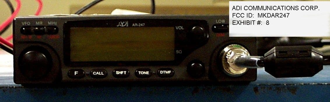
MKDAR247
Nov 03, 1999SCANNING RECEIVER PART OF TRANSCEIVER
Equipment Class
CSR - Scanning Receiver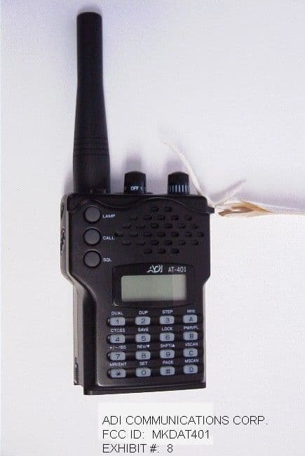
MKDAT401
Sep 16, 1999Scanning Receiver
Equipment Class
CSR - Scanning Receiver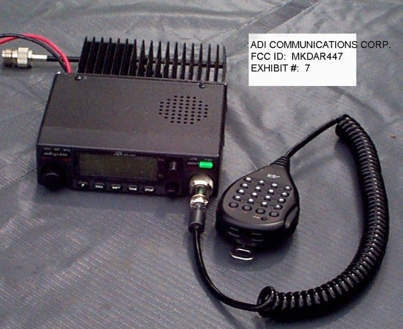
MKDAR447
Jun 21, 1999CSR - Scanning Receiver
Equipment Class
CSR - Scanning ReceiverMKDAT201
Sep 11, 1996CXX - Communications Rcvr for use w/ licensed Tx and CBs
Equipment Class
CXX - Communications Rcvr for use w/ licensed Tx and CBsMKDAT600
Aug 22, 1996CXX - Communications Rcvr for use w/ licensed Tx and CBs
Equipment Class
CXX - Communications Rcvr for use w/ licensed Tx and CBs