FCCID.CO- FCC ID Database
HomeCompaniesEquipment ClassesSearch

© 2026 FCC ID Database. All rights reserved.

AboutContactData sourced from FCC public records
  1. Home/
  2. ASUSTeK COMPUTER INC./
  3. MSQ-GC701D

MSQ-GC701DUSB Wireless Dongle

ASUSTeK COMPUTER INC.
USB Wireless Dongle - FCC ID MSQ-GC701D - ASUSTeK COMPUTER INC.
Click to zoom

Application Details

Equipment Class
DSS - Part 15 Spread Spectrum Transmitter
Date of Grant
Aug 13, 2026
Application Purpose
Original Equipment
Equipment Note
USB Wireless Dongle
Frequency Range
2404.00000000 - 2478.00000000
Company
ASUSTeK COMPUTER INC.
Country
Taiwan

Documents & Files

Select a file to view
Users Manual

↗

Attestation Statements

↗
↗

Cover Letter(s)

↗
↗

External Photos

↗

ID Label/Location Info

↗

Internal Photos

↗

RF Exposure Info

↗
↗
↗
↗
↗

Test Report

↗
↗
↗

Test Setup Photos

↗
↗

Document Text

Text extracted from the exhibit documents filed with the FCC. Open a document above to read the original.

Users Manual

ROG RAIKIRI II PRO PC Wireless Gaming Controller GC701 English ........................................................................................................ 3 ...............................................................................................................................11 Français .................................................................................................... 19 Deutsch ..................................................................................................... 24 4]GGñðυ .................................................................................................... 29 ˂I̍XMRE ...................................................................................................... 34 Dansk ........................................................................................................ 39 Nederlands ............................................................................................... 44 Suomi ........................................................................................................ 49 Magyar ...................................................................................................... 54 Italiano ...................................................................................................... 59 Norsk......................................................................................................... 64 Português ................................................................................................. 69 Polski ........................................................................................................ 79 6SQʜRʹ .................................................................................................... 84 Slovenský .................................................................................................. 89 Svenska .................................................................................................... 94 ÞñχσϏôψþñσ ............................................................................................... 99 Port ......................................................................................................... 104 Português do Brasil ............................................................................... 109 ÞñχσϏ ....................................................................................................... 114 ..................................................................................................... 119 ߭ଞ˲ ..................................................................................................... 124 ̔˫˶ .......................................................................................................... 129 Türkçe ..................................................................................................... 134 Q27846 / First Edition / August 2026 ΔϳΑέόϟ΍ ʺʩʸʡʲ ROG RAIKIRI II PRO PC wireless gaming controller3 English Wireless Gaming Controller ROG RAIKIRI II Pro PC Package contents 1 1 x ROG RAIKIRI II PRO PC wireless gaming controller 7 2 x Replacement thumbstick modules 2 1 x Charging dock 8 1 x ROG bag 3 1 x USB wireless dongle 9 4 x Rear button covers 4 1 x Stand holder set 10 1 x USB Type-C ® cable 5 1 x Thumbstick module puller 11 Technical documents 6 2 x Replacement thumbstick caps Warranty Card 1 2 3 4 5 6 7 8 9 10 11 Quick Start Guide4 Device features Top view Bottom view 1 2 3 4 5 6 8 9 11 1 2 10 10 12 12 13 14 15 16 16 15 14 1718 19 English ROG RAIKIRI II PRO PC wireless gaming controller5 Enabling/Disabling Selectable Step Triggers You can enable the switches to shorten the travel distance of the left and right triggers by sliding the switches outwards. To go back to full trigger mode, simply slide the switches inwards. Short trigger mode 1 Thumbsticks 11 Display control button 2 ROG Aura RGB LED 12 Bumpers (LB/RB) 3 Hybrid D-pad 13 Pairing button 4 Power button 14 Triggers (LT/RT) 5 View button 15 Step trigger switches 6 Display panel 16 Multi-functional rear buttons (M1/M2/M3/M4) 7 Menu button 17 Pogo pin 8 ROG logo 18 USB dongle with cover 9 ABXY buttons 19 Connection switch 10 F keys (F1/F2/F3/F4) English Quick Start Guide6 Full trigger mode Getting started PC Connect to PC Via wired connection 1. Set the connection switch to USB mode. 2. Connect your controller to the PC with the bundled USB Type-C ® cable, and the controller will automatically power on. English ROG RAIKIRI II PRO PC wireless gaming controller7 Via 2.4GHz 1. Set the connection switch to 2.4GHz mode. 2. Open the dongle cover on the back of the controller to pick up the bundled USB dongle. 3. Insert the USB dongle into an available USB port on your PC. 4. Press the power button on your controller to power it on. Via Bluetooth 1. Set the connection switch to Bluetooth mode. 2. Press the power button on your controller to power it on. 3. Press and hold the pairing button until the display panel displays “Pairing...”, indicating that the controller has started pairing. 4. Find the Bluetooth icon on the task bar on your PC, then click Add a device > ROG RAIKIRI II PRO PC > Finish. 5. The display panel displays “Pairing successful”, indicating that the controller has been connected to the PC successfully. NOTE: • Your controller will automatically pair with the previously paired PC. • If pairing is not successful within 1 minute, the F keys indicator will turn off. • IOS and macOS devices are not supported for Bluetooth connection. 6. Execute the driver for installation. NOTE: Download and install the driver from https://rog.asus.com/controllers-group/. English Quick Start Guide8 On-screen control settings With display control button You can press and hold the display control button for 3 seconds to enter or exit the on-screen control menu. When enabled, use the left or right buttons on the L]FVMH(TEHXSREZMKEXIXLVSYKLSTXMSRW4VIWW%XSGSRƼVQEWIPIGXMSRSVTVIWW B to go back. ƍ 4VSƼ…

Text truncated - open the document above for the full version.

RF Exposure Info

Report No.: 2650033R-SAUSV01S-A Page: 1 of 2 Appendix B. Highest Measurement Data Report No.: 2650033R-SAUSV01S-A Page: 2 of 2 Test Laboratory: DEKRA Date: 2026/07/06 2_RF2.4GHz_2.4G Wireless-4M_CH2_Front_5mm_ANT Main Communication System: UID 0, RF 2.4G; Frequency: 2406 MHz Communication System PAR: 0 dB Medium parameters used: f = 2406 MHz; σ = 1.76 S/m; ε r = 39.35; ρ = 1000 kg/m 3 Phantom section: Flat Section Measurement Standard: DASY5 (IEEE/IEC/ANSI C63.19-2011) DASY Configuration: • Probe: EX3DV4 - SN3698; ConvF(6.64, 6.51, 6.41) @ 2406 MHz; Calibrated: 2025/11/27 • Sensor-Surface: 1.4mm (Mechanical Surface Detection) • Electronics: DAE4 Sn1207; Calibrated: 2025/11/13 • Phantom: ELI 5.0; Type: QDOVA002AA; Serial: 1199 • Measurement SW: DASY52, Version 52.10 (4); Configuration/Flat/Area Scan (8x11x1): Measurement grid: dx=12mm, dy=12mm Maximum value of SAR (measured) = 0.120 W/kg Configuration/Flat/Zoom Scan (7x7x7)/Cube 0: Measurement grid: dx=5mm, dy=5mm, dz=5mm Reference Value = 9.950 V/m; Power Drift = 0.02 dB Peak SAR (extrapolated) = 0.183 W/kg SAR(1 g) = 0.100 W/kg; SAR(10 g) = 0.048 W/kg Smallest distance from peaks to all points 3 dB below = 9.1 mm Ratio of SAR at M2 to SAR at M1 = 56.4% Maximum value of SAR (measured) = 0.155 W/kg

Test Setup Photos

Report No.: 2650033R-SAUSV01S-A Page : 1 of 4 Appendix C. Test Setup Photographs EUT Back_5mm EUT Back(NB)_5mm 5mm 5mm Report No.: 2650033R-SAUSV01S-A Page : 2 of 4 EUT Front_5mm EUT Left-side_5mm 5mm 5mm Report No.: 2650033R-SAUSV01S-A Page : 3 of 4 EUT Right-side_5mm EUT Right-side(NB)_5mm 5mm 5mm Report No.: 2650033R-SAUSV01S-A Page : 4 of 4 EUT Tip_5mm Depth of the liquid in the phantom 5mm

Test Setup Photos

Report No.: 2650033R-RFUSV01S-A Page : 15 of 17 Appendix G. Test Result of Test Setup Photograph Front View of AC Power Line Conducted Emission Test Back View of AC Power Line Conducted Emission Test Report No.: 2650033R-RFUSV01S-A Page : 16 of 17 Radiated Test (Below 1 GHz) Radiated Test (Above 1 GHz) Report No.: 2650033R-RFUSV01S-A Page : 17 of 17 Radiated Test (Above 1 GHz)

Test Report

1/11 承 認 書 SPECIFICATION FOR APPROVAL 客戶名稱 CUSTOMER : 客戶料號 CUSTOMER’S P/N : 料號 PART NUMBER : WAN228010H2451SH06 規格 DESCRIPTION : Chip Antenna 8010 MH-Ant 2.4~2.5G Type H06 版本 VERSION : V1.0 日期 ISSUE DATE : 2026/04/29 客 戶 承 認 CUSTOMER APPROVED 工 程 部 R&D CENTER 承 認 APPROVAL 確 認 CHECKED 製 作 DRAWN Ray Tennyson Snow 萬誠科技股份有限公司 OneWave Electronic Co., Ltd. 112台北市北投區立功街151號1樓 1F, No. 151, Li Gong Street, Beitou District, Taipei City 112, Taiwan 電話: (02) 2898-2220 TEL: +886 2 2898-2220 傳真: (02) 2898-5055 FAX: +886 2 2898-5055 2/11 ONEWAVE TECHNOLOGY CO., LTD. 8010 Chip antenna For Bluetooth / WLAN Applications Dimension (mm) L 8.01 ± 0.20 W 1.03 ± 0.20 T 0.70 ± 0.20 P/N: WAN228010H2451SH06 3/11 ONEWAVE TECHNOLOGY CO., LTD. Part Number Information WAN 22 8010 H 245 1S H 06 A G B C D H E F A Product Series Antenna B Dimension L x W 8.0X1.0mm (+-0.2mm) C Material High K material D Working Frequency 2.4 ~ 2.5GHz E Feeding mode Monopole & Single Feeding F Antenna type Type = 06 G、H Internal Code 1. Electrical Specification Remark : Bandwidth & Peak Gain was measured under evaluation board of next page Specification Part Number WAN228010H2451SH06 Central Frequency 2450 MHz Bandwidth 100 (Min.) MHz Return Loss -10 (Max) dB Peak Gain -0.46 dBi Impedance 50 Ohm Operating Temperature -40~+110 °C Maximum Power 4 W Resistance to Soldering Heats 10 ( @ 260°C) sec. Polarization Linear Azimuth Beamwidth Omni-directional Termination Cu / Sn (Leadless) 4/11 ONEWAVE TECHNOLOGY CO., LTD. 2. PCB Appearance Suggested Matching Circuit 重要資訊 : 匹配元件建議使用精準度高的電感±0.1~0.3nH、電容±0.1pF 5/11 ONEWAVE TECHNOLOGY CO., LTD. 3. Measurement Results Return Loss 6/11 ONEWAVE TECHNOLOGY CO., LTD. Radiation Pattern Efficiency Peak Gain 2400MHz 31.40 % -1.01 dBi 2410MHz 34.91% -0.53 dBi 2420MHz 33.90 % -0.61 dBi 2430MHz 34.86% -0.46 dBi 2440MHz 32.66% -0.73 dBi 2450MHz 32.99 % -0.67 dBi 2460MHz 33.10% -0.66 dBi 2470MHz 34.26% -0.54 dBi 2480MHz 34.72 % -0.51 dBi 2490MHz 33.36% -0.74 dBi 2500MHz 32.83 % -0.86 dBi Y Z X 7/11 ONEWAVE TECHNOLOGY CO., LTD. Chamber Coordinate System 8/11 ONEWAVE TECHNOLOGY CO., LTD. 4.Reliability and Test Condictions ITEM REQUIREMENTS TEST CONDITION Solderability 1. Wetting shall exceed 90% coverage 2. No visible mechanical damage Pre-heating temperature:150°C/60sec. Solder temperature:230±5°C Duration:4±1sec. Solder:Sn-Ag3.0-Cu0.5 Flux for lead free: rosin Solder heat Resistance 1. No visible mechanical damage 2. Central Freq. change :within ± 6% 10±0.5 sec. 60sec .. TEMP (°C) 150°C 260°C Pre-heating temperature:150°C/60sec. Solder temperature:260±5°C Duration:10±0.5sec. Solder:Sn-Ag3.0-Cu0.5 Flux for lead free: rosin Component Adhesion (Push test) 1. No visible mechanical damage The device should be reflow soldered(230±5°C for 10sec.) to a tinned copper substrate A dynometer force gauge should be applied the side of the component. The device must with-ST-F 0.5 Kg without failure of the termination attached to component. Component Adhesion (Pull test) 1. No visible mechanical damage Insert 10cm wire into the remaining open eye bend ,the ends of even wire lengths upward and wind together. Terminal shall not be remarkably damaged. Thermal shock 1. No visible mechanical damage 2. Central Freq. change :within ±6% Phase Temperature(°C) Time(min) 1 +110±5°C 30±3 2 Room Temperature Within 3sec 3 -40±2°C 30±3 4 Room Temperature Within 3sec +110°C=>30±3min -40°C=>30±3min Test cycle:10 cycles The chip shall be stabilized at normal condition for 2~3 hours before measuring. Resistance to High Temperature 1. No visible mechanical damage 2. Central Freq. change :within ±6% 3. No disconnection or short circuit. Temperature: +110±5°C Duration: 1000±12hrs The chip shall be stabilized at normal condition for 2~3 hours before measuring. Resistance to Low Temperature 1. No visible mechanical damage 2. Central Freq. change :within ±6% 3. No disconnection or short circuit. Temperature:-40±5°C Duration: 1000±12hrs The chip shall be stabilized at normal condition for 2~3 hours before measuring. Humidity 1. No visible mechanical damage 2. Central Freq. change :within ±6% 3. No disconnection or short circuit. Temperature: 40±2°C Humidity: 90% to 95% RH Duration: 1000±12hrs The chip shall be stabilized at normal condition for 2~3 hours before measuring. 4±1 sec. 60sec TEMP (°C) 150°C 230°C 9/11 ONEWAVE TECHNOLOGY CO., LTD. 5.Soldering and Mounting Mildly activated rosin fluxes are preferred. The minimum amount of solder can lead to damage from the stresses caused by the difference in coefficients of expansion between solder, chip and substrate. The terminations are suitable for all wave and re-flow soldering systems. If hand soldering cannot be avoided, the preferred technique is the utilization of hot air soldering tools. Recommended temperature profiles for re-flow soldering in Figure 1. Products attachment with a soldering iron is discouraged due to the inherent process control limitations. In the event that a soldering iron must be employed the following precautions are recommended. ‧Preheat circuit and products to 150°C ‧Never contact the ceramic with the iron tip ‧Use a 20 watt soldering iron with tip diameter of 1.0mm ‧280°C tip temperature (max) ‧1.0mm tip diameter (max) ‧Limit soldering time to 3 sec. SOLDERING COOLING NATURAL PRE-HEATING TEMPERATURE(°C) 60~120 s 10s max. 30~60s 250~260 230 180 150 TIME(sec.) Reflow Soldering SOLDERING COOLING NATURAL PRE-HEATING TEMPERATURE(°C) within 3s Gradualcooling 150 TIME(sec.) Iron Soldering Over 60s 350 300 10/11 ONEWAVE TECHNOLOGY CO., LTD. 6.Packaging Information ◆ Tape Specification: W Ao Bo Ko P F E D D1 Po P2 t 16.0 ±0.30 1.30 ±0.10 8.30 ±0.10 1.40 ±0.10 4.00 ±0.10 7.50 ±0.10 1.75 ±0.10 1.50 ±0.10 0.00 ±0.10 4.00 ±0.10 2.00 ±0.10 0.30 ±0.05 ◆ Reel Specification: (7’’, Φ180 mm) Tape Width(mm) A(mm) B(mm) C(mm) D(mm) Chip/Reel(pcs) 16 16±1.0 60±2 13.5±0.5 178±2 3000 11/11 ONEWAVE TECHNOLOGY CO., LTD. 7.Storage and Transportation Information Storage Conditions To maintain the solderab…

Text truncated - open the document above for the full version.

Test Report

Report No.: 2650033R-RFUSV01S-B Page: 1 of 24 Test Report No: 2650033R-RFUSV01S-B TEST REPORT FCC Rules & Regulations Product Name USB Wireless Dongle Brand Name ASUS Model No. GC701D FCC ID MSQ-GC701D Applicant ́s Name / Address ASUSTeK COMPUTER INC. 1F., No. 15, Lide Rd., Beitou, Taipei, 112 Taiwan Manufacturer’s Name ASUSTeK COMPUTER INC. Test Method Requested, Standard FCC CFR Title 47 Part 15 Subpart C Section 15.247 Verdict Summary IN COMPLIANCE Documented by Genie Chang Approved by Steven Tsai Date of Receipt 2026/05/05 Date of Issue 2026/07/07 Report Version V1.0 Report No.: 2650033R-RFUSV01S-B Page: 2 of 24 INDEX page Competences and Guarantees ................................................................................................................................ 4 General Conditions .................................................................................................................................................. 4 Revision History ....................................................................................................................................................... 5 Summary of Test Result .......................................................................................................................................... 6 1. General Information .................................................................................................................................. 7 1.1. EUT Description ....................................................................................................................................... 7 1.2. EUT Information ....................................................................................................................................... 8 1.3. Testing Applied Standards ........................................................................................................................ 8 1.4. Testing Location Information .................................................................................................................... 9 1.5. Ambient Conditions In The Laboratory ................................................................................................... 10 1.6. Measurement Uncertainty ...................................................................................................................... 10 1.7. List of Test Equipment ............................................................................................................................ 11 2. Test Configuration of EUT ...................................................................................................................... 12 2.1. Test Condition ......................................................................................................................................... 12 2.2. Test Frequency Mode ............................................................................................................................. 12 2.3. Duty Cycle .............................................................................................................................................. 12 2.4. Measurement Configuration ................................................................................................................... 13 2.5. Tested System Details ............................................................................................................................ 14 2.6. Configuration of Tested System ............................................................................................................. 14 3. AC Power Line Conducted Emission ..................................................................................................... 15 3.1. Test Setup ............................................................................................................................................... 15 3.2. Test Limit ................................................................................................................................................ 15 3.3. Test Procedure ....................................................................................................................................... 15 3.4. Test Result of AC Power Line Conducted Emission ............................................................................... 15 4. Occupied Bandwidth & 20dB Bandwidth ................................................................................................ 16 4.1. Test Setup ............................................................................................................................................... 16 4.2. Test Limit ................................................................................................................................................ 16 4.3. Test Procedures ...................................................................................................................................... 16 4.4. Test Result of Occupied Bandwidth & 20dB Bandwidth ......................................................................... 16 5. Carrier Frequency Separation ................................................................................................................ 17 5.1. Test Setup ............................................................................................................................................... 17 5.2. Test Limit ................................................................................................................................................ 17 5.3. Test Procedures ...................................................................................................................................... 17 5.4. Test Result of Carrier Frequency Separation ......................................................................................... 17 6. Maximum Peak Conducted Output Power .....................................................…

Text truncated - open the document above for the full version.

Test Report

Report No.: 2650033R-RFUSV01S-B Page : 1 of 22 Appendix A. Test Result of AC Power Line Conducted Emission TX_2M_2440MHz_Line TX_2M_2440MHz_Neutral Report No.: 2650033R-RFUSV01S-B Page : 2 of 22 Appendix B. Test Result of Occupied Bandwidth & 20dB Bandwidth Modulation Frequency (MHz) 99% Occupied Bandwidth (MHz) 20dB Bandwidth (MHz) Limit (MHz) 99% Occupied Bandwidth 20dB Bandwidth GFSK(ULL2M) 2404 2.13 2.37 - - 2440 2.12 2.38 - - 2478 2.12 2.38 - - Report No.: 2650033R-RFUSV01S-B Page : 3 of 22 For 99% Occupied Bandwidth: GFSK(ULL2M)/2404 MHz/Ch1/Ant.1 GFSK(ULL2M)/2440 MHz/Ch19/Ant.1 GFSK(ULL2M)/2478 MHz/Ch38/Ant.1 Report No.: 2650033R-RFUSV01S-B Page : 4 of 22 For 20dB Bandwidth: GFSK(ULL2M)/2404 MHz/Ch1/Ant.1 GFSK(ULL2M)/2440 MHz/Ch19/Ant.1 GFSK(ULL2M)/2478 MHz/Ch38/Ant.1 Report No.: 2650033R-RFUSV01S-B Page : 5 of 22 Appendix C. Test Result of Carrier Frequency Separation Modulation Frequency (MHz) Measure Level (MHz) Limit (MHz) Result GFSK (ULL2M) 2404 2.00 1.580 Pass 2440 2.00 1.583 Pass 2478 2.00 1.583 Pass Report No.: 2650033R-RFUSV01S-B Page : 6 of 22 GFSK(ULL2M) / 2404 MHz GFSK(ULL2M) / 2440 MHz GFSK(ULL2M) / 2478 MHz Report No.: 2650033R-RFUSV01S-B Page : 7 of 22 Appendix D. Test Result of Maximum Peak Conducted Output Power Modulation Frequency (MHz) Maximum Peak Conducted Output Power (dBm) Limit (dBm) Result GFSK (ULL2M) 2404 10.10 21.00 Pass 2440 10.06 21.00 Pass 2478 10.08 21.00 Pass Report No.: 2650033R-RFUSV01S-B Page : 8 of 22 Appendix E. Test Result of Number of Hopping Frequency GFSK (ULL2M) Frequency (MHz) Measure Level (Channels) Limit (Channels) 2404.0 ~ 2478.0 37 ≧ 15 Report No.: 2650033R-RFUSV01S-B Page : 9 of 22 GFSK(ULL2M) / 2404 MHz GFSK(ULL2M) / 2478 MHz Report No.: 2650033R-RFUSV01S-B Page : 10 of 22 Appendix F. Test Result of Dwell Time Modulation Occupancy Time of Frequency Hopping System GFSK (ULL2M) A) 2404 MHz Test Time Period: 0.4*37=14.80 sec, Time slot length :1.073 = 0.001073 sec Dwell Time : 0.001073 *14* 14.8= 0.222 sec。 B) 2440 MHz Test Time Period: 0.4*37=14.80 sec, Time slot length :1.073 = 0.001073 sec Dwell Time : 0.001073 *14* 14.8= 0.222 sec。 C) 2478 MHz Test Time Period: 0.4*37=14.80 sec, Time slot length :1.073 = 0.001073 sec Dwell Time : 0.001073 *14* 14.8= 0.222 sec。 Test Result: The occupancy time of each highest, middle and lowest channel is less than 0.4 sec, and corresponds to the standard. Report No.: 2650033R-RFUSV01S-B Page : 11 of 22 GFSK(ULL2M) / 2404 MHz GFSK(ULL2M) / 2404 MHz-1 GFSK(ULL2M) / 2404 MHz-2 GFSK(ULL2M) / 2440 MHz GFSK(ULL2M) / 2440 MHz-1 GFSK(ULL2M) / 2440 MHz-3 Report No.: 2650033R-RFUSV01S-B Page : 12 of 22 GFSK(ULL2M) / 2478 MHz GFSK(ULL2M) / 2478 MHz-1 GFSK(ULL2M) / 2478 MHz-2 Report No.: 2650033R-RFUSV01S-B Page : 13 of 22 Appendix G. Test Result of Antenna Port Conducted Emission GFSK(ULL2M) / 2404 MHz GFSK(ULL2M) / 2440 MHz GFSK(ULL2M) / 2478 MHz Report No.: 2650033R-RFUSV01S-B Page : 14 of 22 GFSK(ULL2M) (Band Edge) / 2404 MHz GFSK(ULL2M) (Band Edge) / 2478 MHz GFSK(ULL2M) (Band Edge Hopping) / 2404 MHz GFSK(ULL2M) (Band Edge Hopping) / 2478 MHz Report No.: 2650033R-RFUSV01S-B Page : 15 of 22 Appendix H. Test Result of Radiated Emission TX_2M_2404MHz_H TX_2M_2404MHz_V TX_2M_2440MHz_H TX_2M_2440MHz_V Report No.: 2650033R-RFUSV01S-B Page : 16 of 22 TX_2M_2478MHz_H TX_2M_2478MHz_V TX_2M_2440MHz_H TX_2M_2440MHz_V Report No.: 2650033R-RFUSV01S-B Page : 17 of 22 TX_2M_2404MHz_H_Peak TX_2M_2404MHz_V_Peak TX_2M_2478MHz_H_Peak TX_2M_2478MHz_V_Peak Report No.: 2650033R-RFUSV01S-B Page : 18 of 22 Horizontal Polarization for Average Detector: Modulation Channel (MHz) Frequency (MHz) Peak Measurement (dBμV/m) Duty Cycle Factor (dB) Measurement Level (dBμV/m) Margin (dB) Limit (dBμV/m) GFSK (2 Mbps) 2404 2320.2 58.73 -39.172 19.558 -34.442 54 2403.6 105.01 -39.172 65.838 - -- 2478 2478.6 104.86 -39.172 65.688 - -- 2497 58.89 -39.172 19.718 -34.282 54 Vertical Polarization for Average Detector: Modulation Channel (MHz) Frequency (MHz) Peak Measurement (dBμV/m) Duty Cycle Factor (dB) Measurement Level (dBμV/m) Margin (dB) Limit (dBμV/m) GFSK (2 Mbps) 2404 2357 59.43 -39.172 20.258 -33.742 54 2403.6 102.68 -39.172 63.508 -- -- 2478 2478.6 104.52 -39.172 65.348 - -- 2489.2 59.08 -39.172 19.908 -34.092 54 Report No.: 2650033R-RFUSV01S-B Page : 19 of 22 Worst-Case Emissions Above 18 GHz TX_2M_2440MHz_H TX_2M_2440MHz_V

Attestation Statements

Covered List Attestation Letter Date: July 28, 2026 FCC ID: MSQ-GC701D To: Federal Communications Commission 7435 Oakland Mills Road Columbia, MD 21046 USA To Whom It May Concern: Attestation Sections 2.911(d)(5) of the FCC Rules (KDB 986446 D01 Covered Equipment) Section 2.911(d)(5)(i) ASUSTeK COMPUTER INC. (“the applicant”) certifies that the equipment for which authorization is sought is not “covered” equipment prohibited from receiving an equipment authorization pursuant to section 2.903 of the FCC rules. ASUSTeK COMPUTER INC. (“the applicant”) further certifies that no cybersecurity or anti- virus software from Kaspersky Lab, Inc. (or its successors/assignees), including integrated Kaspersky software, is installed in the equipment being certified, pursuant to DA-24-886 and KDB 986446 D01 Guidance § B(2a). Section 2.911(d)(5)(ii) ASUSTeK COMPUTER INC. (“the applicant”) certifies that, as of the date of the filing of the application, the applicant is not identified on the Covered List as defined in § 1.50002 of the Commission’s rules, as an entity that produces covered communications equipment or services, nor as a subsidiary or affiliate of such an entity. If you have any questions, please feel free to contact me. Sincerely, ------------------------------------------------------ Jackson Yen / Associate Vice President ASUSTeK COMPUTER INC.

RF Exposure Info

Report No.: 2650033R-SAUSV01S-A Page: 1 of 2 Appendix A. System Check Data Report No.: 2650033R-SAUSV01S-A Page: 2 of 2 Test Laboratory: DEKRA Date: 2026/07/06 System Performance Check_2450MHz-Head Communication System: UID 0, CW; Frequency: 2450 MHz Communication System PAR: 0 dB Medium parameters used: f = 2450 MHz; σ = 1.81 S/m; ε r = 39.2; ρ = 1000 kg/m 3 Phantom section: Flat Section Measurement Standard: DASY5 (IEEE/IEC/ANSI C63.19-2011) DASY Configuration: • Probe: EX3DV4 - SN3698; ConvF(6.64, 6.51, 6.41) @ 2450 MHz; Calibrated: 2025/11/27 • Sensor-Surface: 1.4mm (Mechanical Surface Detection) • Electronics: DAE4 Sn1207; Calibrated: 2025/11/13 • Phantom: ELI 5.0; Type: QDOVA002AA; Serial: 1199 • Measurement SW: DASY52, Version 52.10 (4); Configuration/2450MHz-Head/Area Scan (8x9x1): Measurement grid: dx=12mm, dy=12mm Maximum value of SAR (measured) = 18.6 W/kg Configuration/2450MHz-Head/Zoom Scan (7x7x7)/Cube 0: Measurement grid: dx=5mm, dy=5mm, dz=5mm Reference Value = 105.1 V/m; Power Drift = 0.11 dB Peak SAR (extrapolated) = 25.2 W/kg SAR(1 g) = 12.9 W/kg; SAR(10 g) = 5.97 W/kg Smallest distance from peaks to all points 3 dB below = 9 mm Ratio of SAR at M2 to SAR at M1 = 57.6% Maximum value of SAR (measured) = 19.6 W/kg

RF Exposure Info

Report No.: 2650033R-SAUSV01S-A Page: 1 of 24 Test report No.: 2650033R-SAUSV01S-A SAR Test Report Product Name USB Wireless Dongle Trademark ASUS Model and /or type reference GC701D Applicant ́s name / address ASUSTeK COMPUTER INC. 1F., No. 15, Lide Rd., Beitou Dist., Taipei City 112, Taiwan Manufacturer ́s name ASUSTeK COMPUTER INC. FCC ID MSQ-GC701D Applicable Standard IEEE 1528-2013 KDB 447498 D01 v06 KDB 865664 D01 v01r04 Test Result Max. SAR Measurement (1g) 2.4 GHz: 0.254 W/kg Verdict Summary IN COMPLIANCE Documented By (Senior Project Specialist / Genie Chang) Tested By (Senior Engineer / Luke Cheng) Approved By (Assistant Manager / San Lin) Date of Receipt 2026/05/05 Date of Issue 2026/07/17 Report Version V1.0 Report No.: 2650033R-SAUSV01S-A Page: 2 of 24 INDEX Page 1. General Information ........................................................................................................ 5 1.1 EUT Description ................................................................................................. 5 1.2 Antenna List ....................................................................................................... 5 1.3 Test Environment ................................................................................................ 6 1.4 Measurement procedures................................................................................... 7 2. SAR Measurement System ............................................................................................. 8 2.1 DASY System Description .................................................................................. 8 2.2 Area Scans ......................................................................................................... 9 2.3 DASY E-Field Probe ......................................................................................... 10 2.4 DATA Acquisition Electronics (DAE) and Measurement Server ........................ 11 2.5 Robot ................................................................................................................ 12 2.6 Device Holder ................................................................................................... 12 2.7 Phantom ........................................................................................................... 13 3. Tissue Simulating Liquid .............................................................................................. 14 3.1 The composition of the tissue simulating liquid ................................................ 14 3.2 Tissue Calibration Result .................................................................................. 14 3.3 Tissue Dielectric Parameters for Phantoms ..................................................... 15 4. Measurement Procedure ............................................................................................... 16 4.1 SAR System Check ..............................................................…

Text truncated - open the document above for the full version.

Contact Information

Applicant

Jackson Yen(Associate Vice President)
[email protected]Fax: +886-2-28987364

Technical Contact

ASUS COMPUTER INTERNATIONALGigi Liu
[email protected]

48720 Kato Road · Fremont, 94538 · United States

Test Firm

DEKRA TESTING AND CERTIFICATION CO., LTD. LinKouMirenda Liao
[email protected]Fax: +886-2-2602-6881

Technical Specifications

#Rule PartsFrequency RangePower Output
115C2.40 GHz - 2.48 GHz10.00 mW
Confidentiality
Long Term
Grant Notes
Output power listed is conducted. The antenna(s) used for this transmitter must not transmit simultaneously with any other antenna or transmitter, except in accordance with FCC multi-transmitter product procedures. The grantee must provide installation and operating instructions for complying with FCC multi-transmitter product procedures. Only those antenna(s) tested with the device or similar antenna(s) with equal or lesser gain may be used with this transmitter. End-users and installers must be provided with transmitter operating conditions for satisfying RF exposure compliance. The highest reported SAR for body transmission exposure condition is 0.25W/kg.

Other Applications from ASUSTeK COMPUTER INC.

Wireless Gaming Controller - FCC ID MSQ-GC701 - ASUSTeK COMPUTER INC.
MSQ-GC701

Wireless Gaming Controller

Aug 21, 2026

Equipment Class

DSS - Part 15 Spread Spectrum Transmitter
MSQMPDONGLE3

WIRELESS DONGLE

Aug 18, 2026

Equipment Class

DTS - Digital Transmission System
MSQ-CM3206DM4A

Chromebook/Notebook PC

May 27, 2026

Equipment Class

DCD - Part 15 Low Power Transmitter Below 1705 kHz
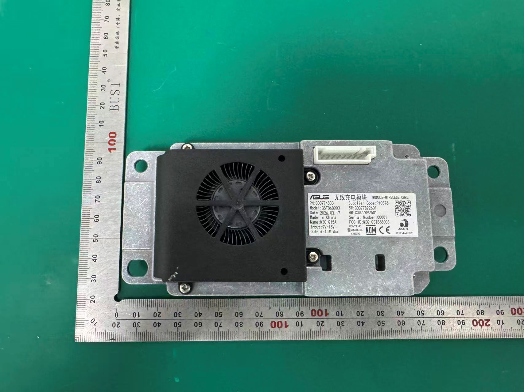
MODULE-WIRELESS CHRG - FCC ID MSQ-GST868003 - ASUSTeK COMPUTER INC.
MSQ-GST868003

MODULE-WIRELESS CHRG

Apr 03, 2026

Equipment Class

DCD - Part 15 Low Power Transmitter Below 1705 kHz
MSQHT7407NA

ProArt PZ14 Keyboard

Mar 18, 2026

Equipment Class

DTS - Digital Transmission System