N6C-WDCD3310Wireless E84 Digital Communication Device
Silex Technology, Inc.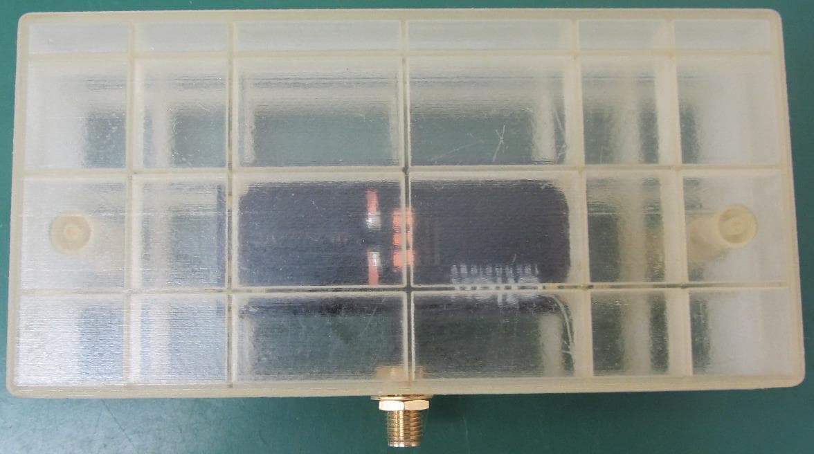
Click to zoom
Application Details
- Equipment Class
- NII - Unlicensed National Information Infrastructure TX
- Date of Grant
- Aug 30, 2020
- Application Purpose
- Original Equipment
- Date of Application
- Aug 30, 2020
- Equipment Note
- Wireless E84 Digital Communication Device
- Frequency Range
- 5726.00000000 - 5825.00000000
- Company
- Silex Technology, Inc.
- Country
- Japan
Documents & Files
Document Text
Text extracted from the exhibit documents filed with the FCC. Open a document above to read the original.
Users Manual
Wireless E84 Digital Communication Device(WDCD-3310)User Manual WDCD-3310 is a device that E84 interlock communication by wireless communication during FOUP transfer between the OHT(Overhead Hoist Transfer)and semiconductor manufacturing equipment. The WDCD-3310 is equipped on the semicunductor manufacturing equipment. Parts and Functions STATUS LED Red light on : Hardware error Green light on : Power On Orange light on : Setting various parameters of wireless E84 device via tool Red light on : Wireless E84 device parameter setting error via tool POWER LED Green light on : Power On Green light flashing : Program changing Orange light on : Initializing process W-E84 LED Orange light on : Power On(5.8GHz) Orange light flashing : Communicating in the 5.8 GHz band Red light on : An error occurred in communication with the wireless E84 unit Green light on : Power On(2.4GHz) Green light flashing : Communicating in the 2.4 GHz band Antenna connector 5pin connector micro USB 3pin connector DIP Switch 12pin connector 10pin connector Push Switch POWER LED STATUS LED W-E84 LED 3pin connector 5pin connector 10pin connector 12pin connector Micro USB Antenna connector Push Switch Setup 2.Powered by semiconductor manufacturing equipment and controls WDCD-3310. Basic configration Wireless Frequency Band Wireless Channel Wireless Channel Width Channel Power setting Channel Period Receive timeout Commnication timeout Pairing threshold level Specification Power supply Wireless I/F Push Switch Ch3~Ch80(2.4GHz) Ch2~Ch100(5.8GHz) 1MHz Connect the antenna Used to initialization settings Debug port ISM(2.4GHz,5.8GHz) -20dBm~0dBm(2.4GHz) -20dBm~+2dBm(5.8GHz) 10,20,30,40,50ms 100~60000ms 100~5000ms -80~-24dBm、No threshold Debug port CPU internal ROM writing (only used in the factory) Connect to semicondutor manufacturing equipment 1.Use a dedicated cable to connect the 10-pin & 12-pin connector to semiconductor manufacturing equipment. Connect to semicondutor manufacturing equipment 0~+40°C Humidity20~80%RH(Non condensing) Strorage environment Temperature -10~+50°C Humidity20~90%RH(Non condensing) Operating environment Temperature DC24V short-range wireless(2.4GHz/5.8GHz) initializaition swtich ×1 LEDPOWER LED Green/Red/Orange STATUS LED Green/Red/Orange W-E84 LED Green/Red/Orange Supplier's Declaration of Conformity 47 CFR § 2.1077 Compliance Information Unique Identifier: WDCD-3310 Responsible Party – U.S. Contact Information Responsible Party Name: silex technology America, Inc. Responsible Party Address: East Sandpointe, #245 Santa Ana, CA 92707 Phone: 657-218-5199 FCC Compliance Statement This device complies with part 15 of the FCC Rules. Operation is subject to the following two conditions: (1) This device may not cause harmful interference, and (2) this device must accept any interference received, including interference undesired operation. FCC CAUTION Changes or modifications not expressly approved by the party responsible for compliance could void the user's authority to operate the equipment. Note: This equipment has been tested and found to comply with the limits for a Class A digital device, pursuant to part 15 of the FCC Rules. These limits are designed to provide reasonable protection against harmful interference when the equipment is operated in a commercial environment. This equipment generates, uses, and can radiate radio frequency energy and, if not installed and used in accordance with the instruction manual, may cause harmful interference to radio communications. Operation of this equipment in a residential area is likely to cause harmful interference in which case the user will be required to correct the interference at his own expense. Compliance with FCC requirement 15.407© Data transmission is always initiated by software, which is the passed down through the MAC, through the digital and analog baseband, and finally to the RF chip. Several special packets are initiated by the MAC. These are the only ways the digital baseband portion will turn on the RF transmitter, which it then turns off at the end of the and can radiate radio frequency energy and, if not installed and used in accordance with the instruction packet. Therefore, the transmitter will be on only while one of the aforementioned packets is being transmitted. In other words, this device automatically discontinue transmission in case of either absence of information to transmit or operational failure. Frequency Tolerance: ±60 ppm This transmitter must not be co-located or operated in conjunction with any other antenna or transmitter. This equipment complies with FCC radiation exposure limits set forth for an uncontrolled environment and meets the FCC radio frequency (RF) Exposure Guidelines as this equipment has very low levels of RF energy.
External Photos
WDCD-3310 External Photos Top Bottom Right Left Front Back 1.Antenna Photograph Model:JUM2458PO_W1 Top Bottom Right Left Front Back Model:JUM2458PO_W1-1 Top Bottom Right Left Front Back 2.Connecting photograph Connection to the WDCD-3310(Using JUM2458PO_W1) Near the RF connector on the WDCD-3310 Near the RF connector on the antenna Connection to the WDCD-3310(Using JUM2458PO_W1-1) Near the RF connector on the WDCD-3310 Near the RF connector on the antenna
ID Label/Location Info
2020/7/6 silex technology, Inc Label design for WDCD-3310 This product is not a product for general retail sale and is installed in a dedicated facility for each country. Once installed and configured to match the country of operation, this product will not be brought into another country.
Internal Photos
2020/7/1 silex technology, Inc WDCD-3310 Internal Photos Before mounting shield After mounting shield Top Bottom
RF Exposure Info
August 3, 2020 FCC ID: N6C-WDCD3310 To whom it may concern, We, UL Japan, Inc, hereby declare that Wireless E84 Digital Communication Device, model: WDCD- 3310 (FCC ID: N6C-WDCD3310) of silex technology, Inc. is exempt from RF exposure SAR evaluation as its output power meets the exclusion limits stated in KDB 447498D01(v06). KDB 447498D01(v06) has the following exclusion for portable devices: The 1g and 10g SAR test exclusion thresholds for 100 MHz to 6 GHz at test separation distances ≤ 50 mm are determined by: [(max. power of channel, including tune-up tolerance, mW)/(min. test separation distance, mm)] ꞏ[√f(GHz)] ≤ 3.0 for 1-g SAR and ≤ 7.5 for 10-g extremity SAR, where •f(GHz) is the RF channel transmit frequency in GHz •Power and distance are rounded to the nearest mW and mm before calculation •The result is rounded to one decimal place for comparison The test exclusions are applicable only when the minimum test separation distance is ≤ 50 mm and for transmission frequencies between 100 MHz and 6 GHz. When the minimum test separation distance is < 5 mm, a distance of 5 mm is applied to determine SAR test exclusion. [2.4 GHz] This device has f = 2.48 GHz and distance = 5 mm (minimum separation distance: 5 mm was used in the calculation) and the maximum average output power was 1 mW So for this device: 1 mW[maximum average output power]/5 mm[minimum separation distance]*√2.48 = 0.3 (This value was calculated as a reference since maximum average output power was less than 1mW.) [5 GHz] This device has f = 5.825 GHz and distance = 5 mm (minimum separation distance: 5 mm was used in the calculation) and the maximum average output power was 2 mW So for this device: 2 mW[maximum average output power]/5 mm[minimum separation distance]*√5.825 = 1.0 *This is less than 3.0, so no SAR is required. Even taking into account the tolerance, this device can be satisfied with the limits. Thank you for your attention to this matter. Satofumi Matsuyama Engineer of Ise EMC Lab. Consumer Technology Division UL Japan, Inc.
Test Report
Test report No. : 13226743H-D-R3 Page : 1 of 41 Issued date : August 31, 2020 FCC ID : N6C-WDCD3310 UL Japan, Inc. Ise EMC Lab. 4383-326 Asama-cho, Ise-shi, Mie-ken 516-0021 JAPAN Telephone : +81 596 24 8999 Facsimile : +81 596 24 8124 Report Cover Page - 13-EM-F0429 Issue # 17.0 RADIO TEST REPORT Test Report No. : 13226743H-D-R3 Applicant : silex technology, Inc. Type of EUT : Wireless E84 Digital Communication Device Model Number of EUT : WDCD-3310 FCC ID : N6C-WDCD3310 Test regulation : FCC Part 15 Subpart E: 2020 Test Result : Complied (Refer to SECTION 3.2) This report contains data that are not covered by the NVLAP accreditation. There is no testing item of "Non-accreditation". 1. This test report shall not be reproduced in full or partial, without the written approval of UL Japan, Inc. 2. The results in this report apply only to the sample tested. 3. This sample tested is in compliance with the limits of the above regulation. 4. The test results in this test report are traceable to the national or international standards. 5. This test report covers Radio technical requirements. It does not cover administrative issues such as Manual or non-Radio test related Requirements. (if applicable) 6. The all test items in this test report are conducted by UL Japan, Inc. Ise EMC Lab. 7. This test report must not be used by the customer to claim product certification, approval, or endorsement by NVLAP, NIST, or any agency of the U.S. Government. 8. The information provided from the customer for this report is identified in Section 1. 9. This report is a revised version of 13226743H-D-R2. 13226743H-D-R2 is replaced with this report. Date of test: March 24 to June 28, 2020 Representative test engineer: Junki Nagatomi Engineer Consumer Technology Division Approved by: Satofumi Matsuyama Engineer Consumer Technology Division This laboratory is accredited by the NVLAP LAB CODE 200572-0, U.S.A. The tests reported herein have been performed in accordance with its terms of accreditation. *As for the range of Accreditation in NVLAP, you may refer to the WEB address, http://japan.ul.com/resources/emc_accredited/ Test report No. : 13226743H-D-R3 Page : 2 of 41 Issued date : August 31, 2020 FCC ID : N6C-WDCD3310 UL Japan, Inc. Ise EMC Lab. 4383-326 Asama-cho, Ise-shi, Mie-ken 516-0021 JAPAN Telephone : +81 596 24 8999 Facsimile : +81 596 24 8124 REVISION HISTORY Original Test Report No.: 13226743H-D Revision Test report No. Date Page revised Contents - (Original) 13226743H-D July 29, 2020 - - 1 13226743H-D-R1 August 20, 2020 P 11 Addition of No.F: Terminal information Addition of ex planatory note *1) 2 13226743H-D-R2 August 26, 2020 P 5 Correction of Receipt Date of Sample in Section2.1 March 11, 2020→ March 11, 2020 (The test data before March 24, 2020 used this samples.) *1) June 9, 2020 (The test data after June 26, 2020 used this samples.) *1) The samples received on March 11, 2020 did not differ from the samples received on June 9, 2020.Therefore, the data for the tests performed with sam ples received on March 11, 2020 was used. 2 13226743H-D-R2 August 26, 2020 P 7 Correction of Test Specification in Section 3.1. FCC Part 15 final revised on May 26, 2020 and effective July 27, 2020 except 15.258→ FCC Part 15 final revised on June 26, 2020 and effective July 27, 2020 Addition of below explanatory note. * The revision does not affect the test result conducted before its effective date. 3 13226743H-D-R3 August 31, 2020 P 5 Correction of explanatory note for Receipt Date of Sample *1) in Section2.1 *1) The samples received on March 11, 2020 did not differ from the samples received on June 9, 2020.Therefore, the data for the tests performed with samples received on March 11, 2020 was used. → *1) The samples received on June 9, 2020 have improved spurious emission characteristics over the samples received on March 11, 2020, due to improvements in the electromagnetic wave absorption sheet. There was no difference in the maximum conducted output power test results between the samples received on March 11, 2020 and the samples received on June 9, 2020, therefore the test data performed with samples received on March 11, 2020 was used for Antenna Terminal Conducted Tests. Test report No. : 13226743H-D-R3 Page : 3 of 41 Issued date : August 31, 2020 FCC ID : N6C-WDCD3310 UL Japan, Inc. Ise EMC Lab. 4383-326 Asama-cho, Ise-shi, Mie-ken 516-0021 JAPAN Telephone : +81 596 24 8999 Facsimile : +81 596 24 8124 Reference: Abbreviations (Including words undescribed in this report) A2LA The American Association for Laboratory Accreditation MCS Modulation and Coding Scheme AC Alternating Current MRA Mutual Recognition Arrangement AFH Adaptive Frequency Hopping N/A Not Applicable AM Amplitude Modulation NIST National Institute of Standards and Technology Amp, AMP Amplifier NS No signal detect. ANSI American National Standards Institute NSA Normalized Site Attenuation Ant, ANT Antenna NVLAP National Voluntary Laboratory Accreditation Program AP Access Point OBW Occupied Band Width ASK Amplitude Shift Keying OFDM Orthogonal Frequency Division Multiplexing Atten., ATT Attenuator P/M Power meter AV Average PCB Printed Circuit Board BPSK Binary Phase-Shift Keying PER Packet Error Rate BR Bluetooth Basic Rate PHY Physical Layer BT Bluetooth PK Peak BT LE Bluetooth Low Energy PN Pseudo random Noise BW BandWidth PRBS Pseudo-Random Bit Sequence Cal Int Calibration Interval PSD Power Spectral Density CCK Complementary Code Keying QAM Quadrature Amplitude Modulation Ch., CH Channel QP Quasi-Peak CISPR Comite International Special des Perturbations Radioelectriques QPSK Quadri-Phase Shift Keying CW Continuous Wave RBW Resolution Band Width DBPSK Differential BPSK RDS Radio Data System DC Direct Current RE Radio Equipment D-factor Distance factor RF Radio Frequency DFS Dynamic Frequency Selection RMS Root Mean Square DQPSK Differential QPSK RSS Radio Standards Specifications DSSS Direct Sequence Spread Spectrum Rx Receiving EDR Enha…
Text truncated - open the document above for the full version.
Test Setup Photos
Test report No. : 13226743H-D-R3 Page : 38 of 41 Issued date : August 31, 2020 FCC ID : N6C-WDCD3310 UL Japan, Inc. Ise EMC Lab. 4383-326 Asama-cho, Ise-shi, Mie-ken 516-0021 JAPAN Telephone : +81 596 24 8999 Facsimile : +81 596 24 8124 APPENDIX 3: Photographs of test setup Conducted Emission Photo 1 Photo 2 Test report No. : 13226743H-D-R3 Page : 39 of 41 Issued date : August 31, 2020 FCC ID : N6C-WDCD3310 UL Japan, Inc. Ise EMC Lab. 4383-326 Asama-cho, Ise-shi, Mie-ken 516-0021 JAPAN Telephone : +81 596 24 8999 Facsimile : +81 596 24 8124 Radiated Spurious Emission Photo 1 Photo 2 Test report No. : 13226743H-D-R3 Page : 40 of 41 Issued date : August 31, 2020 FCC ID : N6C-WDCD3310 UL Japan, Inc. Ise EMC Lab. 4383-326 Asama-cho, Ise-shi, Mie-ken 516-0021 JAPAN Telephone : +81 596 24 8999 Facsimile : +81 596 24 8124 Worst Case Position Below 1 GHz (Horizontal: X-axis/ Vertical:X-axis) Above 1 GHz (Horizontal: X-axis/ Vertical: Z-axis) 10 - 18 GHz (Horizontal: X-axis/ Vertical: X-axis) Antenna X-axis Y-axis Z-axis Test report No. : 13226743H-D-R3 Page : 41 of 41 Issued date : August 31, 2020 FCC ID : N6C-WDCD3310 UL Japan, Inc. Ise EMC Lab. 4383-326 Asama-cho, Ise-shi, Mie-ken 516-0021 JAPAN Telephone : +81 596 24 8999 Facsimile : +81 596 24 8124 Worst Case Position Below 1 GHz (Horizontal: X-axis/ Vertical:X-axis) Above 1 GHz (Horizontal: X-axis/ Vertical: X-axis) 10 - 18 GHz (Horizontal: Z-axis/ Vertical: Y-axis) Module X-axis Y-axis Z-axis End of Report
Contact Information
Applicant
Yoshinori Nakai(General Manager)
Technical Contact
UL Japan, Inc.Satofumi Matsuyama
[email protected]81-596-24-8999
4383-326 Asama-cho, Ise-shi · Mie-ken · Japan
Test Firm
UL Japan, Inc.Masamichi Ishii
Technical Specifications
| # | Rule Parts | Frequency Range | Power Output |
|---|---|---|---|
| 1 | 15E | 5.73 GHz - 5.83 GHz | 1.60 mW |
Other Applications from Silex Technology, Inc.
N6C-SDMAX6E
Mar 26, 2026SX-SDMAX6E
Equipment Class
DTS - Digital Transmission System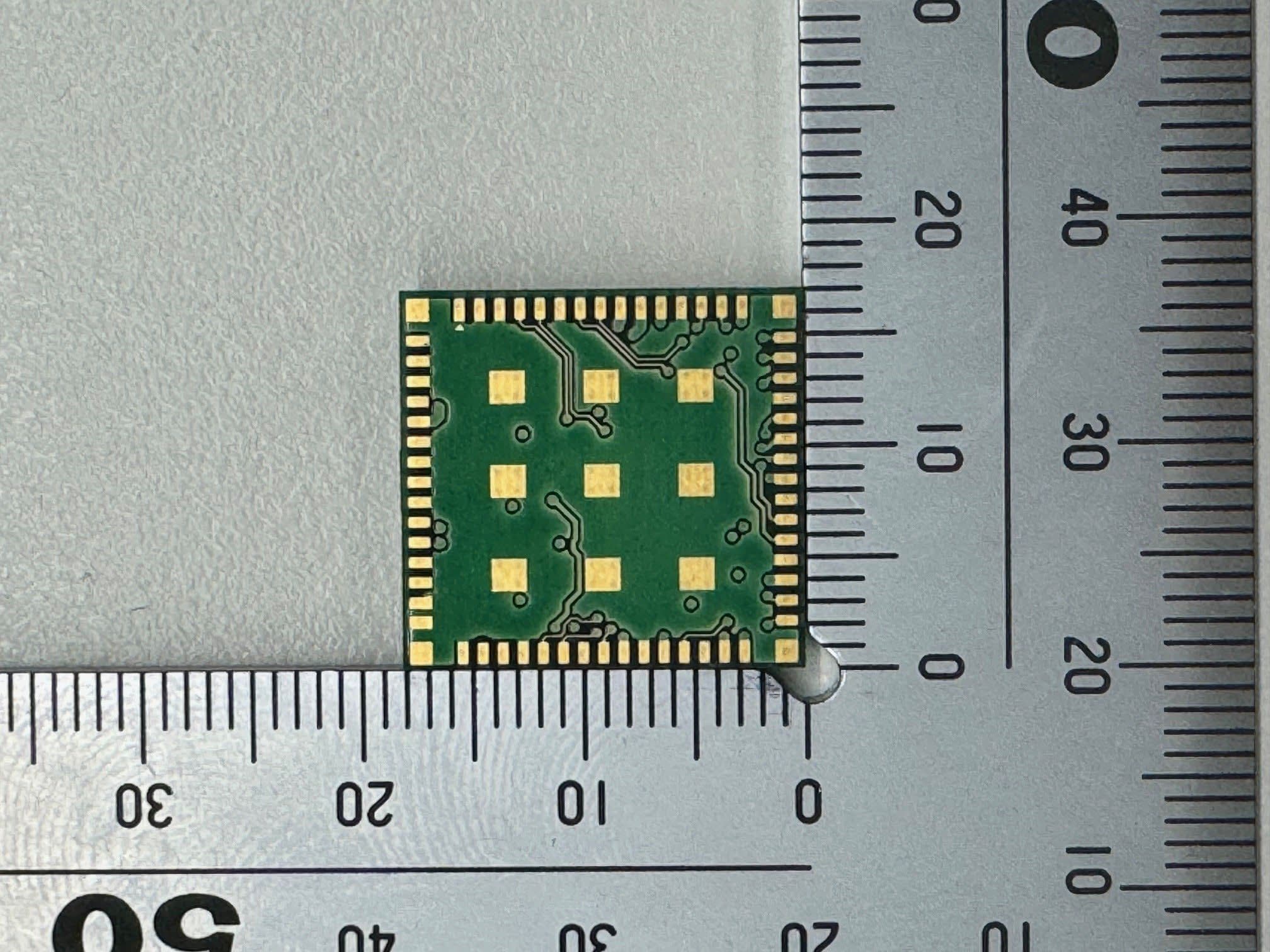
N6C-SDMAH
Feb 04, 2024Embedded Wireless Module
Equipment Class
DTS - Digital Transmission System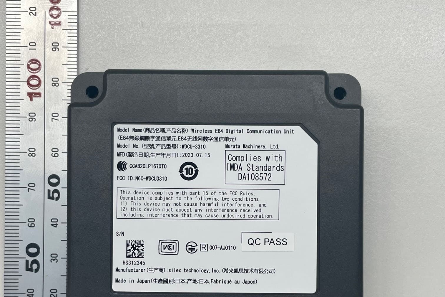
N6C-WDCU3310H
Oct 08, 2023Wireless E84 Digital Communication Unit
Equipment Class
NII - Unlicensed National Information Infrastructure TX
N6C-AP200AC
May 31, 2021Wireless LAN Access Point
Equipment Class
DTS - Digital Transmission System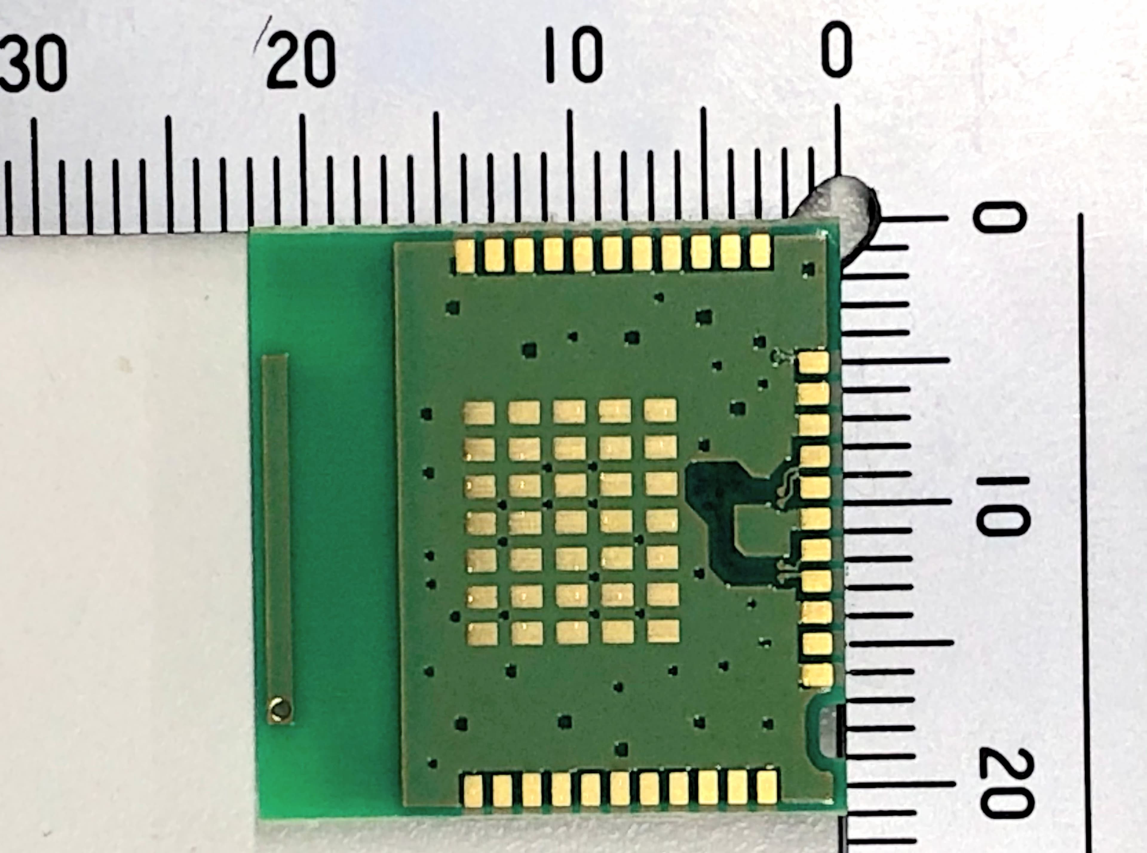
N6C-USBAC
Apr 19, 2021Embedded Wireless Module
Equipment Class
DTS - Digital Transmission System