N6OGSPS-ACT-02
Gemstar Communications Inc
Click to zoom
Application Details
- Equipment Class
- DXX - Part 15 Low Power Communication Device Transmitter
- Date of Grant
- Oct 15, 2000
- Application Purpose
- Original Equipment
- Date of Application
- May 11, 2000
- Frequency Range
- 916.50000000 - 916.50000000
- Company
- Gemstar Communications Inc
- Country
- Canada
Documents & Files
Document Text
Text extracted from the exhibit documents filed with the FCC. Open a document above to read the original.
Users Manual
Technical Manual Radio-Frequency Identification (RFID) Package Reporting and Tracking System Gemstar Communications Inc. 760 Pacific Road, Unit 7, Oakville, Ontario L6L 6M5 Section i - NoticeGemstar Communications Inc. Revision 0 11-May-00Page i Notice Copyright © 1999 Gemstar Communications Inc. ("Gemstar"). The information herein is provided without liability to any user. While every effort has been made to verify the accuracy and completeness of this information, Gemstar makes no guarantee as to its accuracy or applicability for any particular use. In every instance, it is the user's responsibility to determine the suitability of this product for their application. Gemstar reserves the right to revise product hardware, software, or documentation without obligation to notify any person or organization. Nothing contained herein shall be construed as a recommendation to use any product in violation of patents or other rights of third parties. The sale of any Gemstar product is subject to all Gemstar Terms and Conditions of Sale and Sale Policies, copies of which can be provided upon request. This document contains proprietary information which is protected by copyright. All rights are reserved. No part of this document may be copied or reproduced in any form without the express written permission of Gemstar. Trademarks Product names mentioned in this manual may be trademarks, and they are used for identification only. User Comments In order for us to maintain the quality of our publications, we invite our customers to forward comments or suggestions to help us improve the effectiveness of this manual. Part Number 1020050, Revision 0 First Printing: August, 1999 Printed in Canada Section ii - Table of ContentsGemstar Communications Inc. Revision 0 11-May-00Page ii Table of Contents Notice.....................................................................................................................i Table of Contents..................................................................................................ii System Overview.................................................................................................1 System Description...........................................................................................1 Technical Summary..........................................................................................2 Use and Purpose..........................................................................................2 Radio Frequencies........................................................................................4 RF Power Output and Field Strength............................................................4 Time Lines/Duty Cycle..................................................................................4 Regulatory Approval Label Diagram.................................................................6 Component Description........................................................................................9 Lettermail Tag...................................................................................................9 Tag Function.................................................................................................9 Tag Model Numbers....................................................................................10 Tag Diagnostic Lights..................................................................................10 Tag Test Procedure....................................................................................10 Tag Schematic Diagram & Parts List..........................................................11 Activator..........................................................................................................12 Activator Function.......................................................................................12 Activator Model Numbers............................................................................12 Activator Diagnostic Lights..........................................................................13 Activator Schematic Diagram & Parts List...................................................13 MicroCell.........................................................................................................14 MicroCell Function......................................................................................14 MicroCell Model Numbers...........................................................................14 MicroCell Diagnostic Lights.........................................................................15 MicroCell Schematic Diagram & Parts List..................................................15 On-Site Controller...........................................................................................16 On-Site Controller Function.........................................................................16 OSC Model Numbers..................................................................................16 OSC Diagnostic Lights................................................................................17 Maintenance Procedures...................................................................................18 Principles of Operation...................................................................................18 Installation Guide............................................................................................18 Installation Checklist...................................................................................18 Installation Procedures................................................................................20 Performance Specifications............................................................................25 Tag..............................................................................................................25 Activator......................................................................................................25 Mi…
Text truncated - open the document above for the full version.
Users Manual
TDMA Activator Principle of Operation TDMA Activator Principle of Operation Supplementary Manual May 4, 2000 TDMA Activator Principle of Operation TABLE OF CONTENTS INTRODUCTION......................................................................................................................................................3 1-TYPE OF UNITS.....................................................................................................................................................3 1.1-AUTONOMOUS................................................................................................................................................3 1.2-MASTER............................................................................................................................................................3 1.3-SLAVE...............................................................................................................................................................3 2-TIME SLOTS..........................................................................................................................................................3 3-SYNCHRONIZATION...........................................................................................................................................4 4-RE-SYNC and LOSS OF SIGNAL........................................................................................................................4 5-USE OF TIME BLOCKS.......................................................................................................................................4 6-HARDWARE...........................................................................................................................................................6 7-RF DATA FORMAT...............................................................................................................................................7 7.1-ENCODING......................................................................................................................................................7 7.2-SLAVE AND AUTONOMOUS ACTIVATOR DATA SEQUENCE...........................................................7 7.3-MASTER ACTIVATOR DATA SEQUENCE...............................................................................................8 8-KNOWN LIMITATION.........................................................................................................................................8 9-INSTALLATION.....................................................................................................................................................9 9.1-ANTENNA TYPES...........................................................................................................................................9 9.2-POWER SETTING AND ANTENNA GAINS...............................................................................................9 9.2.1-MAX POWER FOR MONO-POLE........................................................................................................9 9.2.2-MAX POWER FOR PATCH...................................................................................................................9 9.3-POWER SETTING AND ADJUSTING.........................................................................................................9 TDMA Activator Principle of Operation INTRODUCTION The TDMA (Time Domain Multiple Access) mode activator system uses a synchronised time keeping system to permit various activators to transmit their signals without causing interference to other activator. This is done by defining time slots and permitting any given activator to transmit only within selected time slots. By insuring no two overlapping activator fields have the same time slot, interference should not be an issue. 1-TYPE OF UNITS There are 3 basic modes the activators can operate in: • 1.1-AUTONOMOUS Operates without regards to time slots. This was the original mode of operation. It has uses where no time base signal can be presented and transmits at all times • 1.2-MASTER There is usually only one master unit in a system. It sends the time base count based on it own internal clock, starting at 1 when reset. The Master only transmits during its selected time blocks. • 1.3-SLAVE This is the most used mode. When the unit operates as a slave it first must receive a valid time base signal from the Master unit to synchronize its internal counter to match the master unit. Once that has happened, it then transmits during its selected time blocks and received time base sync. signals when not in transmit mode. 2-TIME SLOTS Time is split into 6 units, each unit being 40 seconds long. The system repeats the time loop cycle every 240 seconds (4 minutes) That is, the system starts in time block (slot) 1 doing what is programmed for this time block, then moves to time block 2 and so on. At the end of block 6, the system resets back to beginning of block 1. Block 1 Block 2 Block 1Block 2Block 3 Block 4 Block 5Block 6 Repeat loop The Duration of each block was selected based on the fact that the current postal tag wakes up every 32 seconds. By using a time block of 40 seconds, we insure that the postal tag will have two reading every time slot. The control and determination of time blocks or slots is determined by internal time keeping clocks that count from 1 to 240 seconds. Where block 1 is 1 to 40 seconds, block 2 is 41 to 80 seconds and so on. The selection of time block for transmit for each activator is done by a 6 position dip switch. Each pole of the switch represents a single time block. The activator’s processor reads the switch every few seconds and depending if the switch is open or closed for a given time block, the software will either activate the transmitter or receive modes. 3-SYNCHRONIZATION For the system to work, all slaves must have same time count as the master unit. The slave units must not transmit…
Text truncated - open the document above for the full version.
Cover Letter(s)
2 3000 Brsitol Circle, Oakville, Ontario, Canada L6H 6G4 Telephone (905) 829-1570 Facsimile (905) 829-8050 Website: www.ultratech-labs.com Email: [email protected] UltraTech Group of Labs May 4, 2000 FEDERAL COMMUNICATIONS COMMISSION 7435 Oakland Mills Road Columbia, MD 21046 USA Subject: Certification Application under FCC Part 15, Subpart C, Para. 15.249, Low Power Transmitters Operating at 916.5 MHz Frequency. Applicant:GEMSTAR COMMUNICATIONS INC. Product: TDMA Activator Model: GSPS-ACT-02 FCC ID: N6OGSPS-ACT-02 Dear Sir/Madam, As appointed agent for GEMSTAR COMMUNICATIONS INC., please find copy of the engineering report, power of attorney letter, confidential filing letter, and all the necessary items pertaining to this certification application Note that the above mentioned product will be professionally installed by qualified personnel. If you have any queries, please do not hesitate to contact us by our TOLL FREE numbers: OUR TELEPHONE NO.: 1-877-765-4173 Yours truly, Tri Minh Luu, P. Eng., V.P., Engineering TML/AK
Cover Letter(s)
FEDERAL COMMUNICATIONS COMMISION 7435 Oakland Mills Road Columbia, MD 21046 U.S.A. Subject:AUTHORITY TO AT AS AN AGENT TO FEDERAL COMMUNICATIONS COMMISSION. Applicant: Gemstar Communications Inc. Product:TDMA Activator Model:GSPS-ACT-02 FCC ID:N6OGSPS-ACT-02 Dear Sir/Madam, We, Gemstar Communications Inc., hereby appoint Ultratech Engineering Labs Inc. (Ultratech) to act as court agent in the preparation of this application to FCC for authorization of equipment under FCC rules. We also certify that the provided information is properly described the device or system for which authorization is required. If you have any queries, please do not hesitate to contact us. Yours truly, Richard E. Bonham Vice President of Operations
Cover Letter(s)
May 4, 2000 FEDERAL COMMUNICATIONS COMMISSION 7435 Oakland Mills Road Columbia, MD 21046 U.S.A Subject: Request for withholding from public disclosure the schematic diagrams and system block diagrams pursuant to an application for certification. Applicant: Gemstar Communication Inc. Product: TDMA Activator Model: GSPS-ACT-02 FCC ID: N6OGSPS-ACT-02 Dear Sir/Madam, We, Gemstar Communications Inc., would like to request that the schematic diagrams and system block diagrams, submitted with the application for certification be withheld from public disclosure as per Section 0.459 of FCC Rules. This request is made under the provisions of Section 0.457(d) of the Commission’s Rules, and Section 552(b)(4) of the Freedom of Information Act. These sections authorize as a withholding from public inspection materials which would be privileged as a matter of law if retained by the person submitting them, and materials which would not customarily be released to the public by that person. The detailed confidential materials are listed as follows: No. Title Drawing No. Sheet No. 1 TDMA Slave Activator SAX001.sch 1 2 TDMA Slave Activator SAX001.sch 2 3 4 5 If you have any queries, please do not hesitate to contact us by at 905 847 3832. Yours truly, Richard E. Bonham Director of Operations
ID Label/Location Info
TDMA Activator Model No. GSPS--ACT-02 FCCID: N6OGSPS-ACT-02 IC Certification No. IF FOUND PLEASE RETURN TO: GEMSTAR COMMUNICATIONS 760 Pacific Road Unit 7 Oakville Ontario L6L 6M5 Tel: 905 847 3832 This device complies with Part 15 of the FCC Rules. Operation is subject to the following two conditions: (1) this device may not cause harmful interference and (2) this device must accept any interference received, including interference that may cause undesired operation. Made in Canada 1½” (38mm) 2½” (64mm)
Test Report
TDMA Activator MODEL NO.: GSPS-ACT-02 FCC ID: N6OGSPS-ACT-02 FCC PART 15, SUBPART C, PARA. 15.249 LOW POWER TRANSMITTERS OPERATING AT 916.5 MHz UltraTech's FILE NO.: GCI6-FTX TESTED FOR: GEMSTAR COMMUNICATIONS INC. 760 Pacific Road, Unit 7 Oakville, Ontario Canada, L6L 6M5 TESTED BY: UltraTech Engineering Labs Inc. 3000 Brsitol Circle Oakville, Ontario Canada L6H 6G4 PREPARED BY: Dan Huynh DATE: May 4, 2000 UltraTech 3000 Brsitol Circle, Oakville, Ontario, Canada, L6H 6G4 Telephone (905) 829-1570 Facsimile (905) 829-8050 Website: www.ultratech-labs.com Email: [email protected] FCC PART 15, SUBPART C, SEC. 15.249 – INTENTIONAL RADIATORSPage 2 TDMA ActivatorGSPS-ACT-02 ULTRATECH GROUP OF LABSFile #: GCI6-FTX 3000 Bristol Circle, Oakville, Ontario, Canada L6H 6G4May 4, 2000 Tel. #: 905-829-1570, Fax. #: 905-829-8050, Email: [email protected], Website: http://www.ultratech-labs.com • Assessed by ITI (UK) Competent Body, NVLAP (USA) Accreditation Body & ACA/AUSTEL (Australia) • Recognized/Listed by FCC (USA), Industry Canada (Canada) • All test results contained in this engineering test report are traceable to National Institute of Standards and Technology (NIST) TABLE OF CONTENTS 1.EXHIBIT 1 - SUMMARY OF TEST RESULTS & GENERAL STATEMENT OF CERTIFICATION...........3 2.EXHIBIT 2 - GENERAL INFORMATION.............................................................................................................4 2.1.APPLICANT............................................................................................................................................................4 2.2.MANUFACTURER...................................................................................................................................................4 2.3.DESCRIPTION OF EQUIPMENT UNDER TEST............................................................................................................4 2.4.RELATED SUBMITTAL(S)/GRANT...........................................................................................................................5 2.5.TEST METHODOLOGY............................................................................................................................................5 2.6.TEST FACILITY.......................................................................................................................................................5 2.7.UNITS OF MEASUREMENTS....................................................................................................................................5 3.EXHIBIT 3 - SYSTEM TEST CONFIGURATION................................................................................................6 BLOCK DIAGRAMS FOR CONDUCTED & RADIATED EMISSION MEASUREMENTS................................................................6 3.2.PHOTOGRAPH FOR RF EMISSION MEASUREMENTS................................................................................................7 3.2.1.TEST SETUP FOR AC POWER LINE CONDUCTED EMISSIONS MEASUREMENTS............................7 3.2.2.TEST SETUP FOR RADIATED EMISSIONS MEASUREMENTS...............................................................8 3.3.JUSTIFICATION.......................................................................................................................................................9 3.4.EUT OPERATING CONDITION................................................................................................................................9 3.5.SPECIAL ACCESSORIES..........................................................................................................................................9 3.6.EQUIPMENT MODIFICATIONS.................................................................................................................................9 4.EXHIBIT 4 - TEST DATA......................................................................................................................................10 4.1.TRANSMITTER FUNDAMENTAL & HARMONIC RADIATED EMISSIONS @ FCC CFR 47, PARA 15.249(A).............10 4.2.RF EXPOSURE LIMIT FCC 1.1310.......................................................................................................................15 4.3.AC POWERLINE CONDUCTED EMISSIONS, FCC CFR 47, PARA. 15.107(A).........................................................17 5.EXHIBIT 5 - GENERAL TEST PROCEDURES..................................................................................................19 5.1.AC POWERLINE CONDUCTED EMISSIONS MEASUREMENTS - GENERAL TEST METHOD......................................19 5.2.ELECTRICAL FIELD RADIATED EMISSIONS MEASUREMENTS - GENERAL TEST METHOD.....................................20 6.EXHIBIT 6 - INFORMATION RELATED TO EQUIPMENT UNDER TESTS...............................................23 6.1.FCC ID LABELING AND SKETCH OF FCC LABEL LOCATION...............................................................................23 6.2.PHOTOGRAPHS OF EQUIPMENT UNDER TEST........................................................................................................23 6.3.SYSTEM BLOCK DIAGRAM(S)..............................................................................................................................23 6.4.SCHEMATIC DIAGRAMS.......................................................................................................................................23 6.5.USER’S MANUAL WITH “FCC INFORMATION TO USER STATEMENTS”.................................................................23 FCC PART 15, SUBPART C, SEC. 15.249 – INTENTIONAL RADIATORSPage 3 TDMA ActivatorGSPS-ACT-02 ULTRATECH GROUP OF LABSFile #: GCI6-FTX 3000 Bristol Circle, Oakville, Ontario, Canada L6H 6G4May 4, 2000 Tel. #: 905-829-1570, Fax. #: 905-829-8050, Email: [email protected], Website: http://www.ultratech-labs.com • Assessed by ITI (UK) Competent Body, NVLAP (USA) Accreditation Body & ACA/AUSTEL (Australia) • Recognize…
Text truncated - open the document above for the full version.
Test Report
2 3000 Brsitol Circle, Oakville, Ontario, Canada L6H 6G4 Telephone (905) 829-1570 Facsimile (905) 829-8050 Website: www.ultratech-labs.com Email: [email protected] UltraTech Group of Labs May 8, 2000 INDUSTRY CANADA Head, Equipment Approval Unit 3701 Carling Avenue, Bldg. # 94 P.O. Box 11490, Station “H” Ottawa, Ontario K2H 8S2 Subject:Certification Application under Industry Canada RSS-210, Issue Draft 2, Sec. 6.2.2(m2), Low Power Transmitters (916.5 MHz) and Sec. 7 – Radio Receivers (916.5 MHz) Applicant:GEMSTAR COMMUNICATIONS INC. Product:TDMA Activator Model:GSPS-ACT-02 Dear Sir/Madam, As appointed agent for GEMSTAR COMMUNICATIONS INC., please find enclosed copy of the engineering report, application form and a cheque of Cdn $ __________. Note that the above mentioned product will be professionally install by qualified personnel. If you have any queries, please do not hesitate to contact us by our TOLL FREE numbers: OUR TELEPHONE NO.:1-877-765-4173 Yours truly, Tri Minh Luu, P. Eng., V.P., Engineering TML/AK Encl. 2 3000 Brsitol Circle, Oakville, Ontario, Canada L6H 6G4 Telephone (905) 829-1570 Facsimile (905) 829-8050 Website: www.ultratech-labs.com Email: [email protected] UltraTech Group of Labs May 8, 2000 GEMSTAR COMMUNICATIONS INC. 760 Pacific Road, Unit 7 Oakville, Ontario Canada, L6L 6M5 Attn.:Mr. Richard Bonham Subject:Certification Application under Industry Canada RSS-210, Issue Draft 2, Sec. 6.2.2(m2), Low Power Transmitters (916.5 MHz) and Sec. 7 – Radio Receivers (916.5 MHz) Product:TDMA Activator Model:GSPS-ACT-02 Dear Mr. Bonham, The product sample, as provided by you, has been tested and found to comply with Certification Application under Industry Canada RSS-210, Issue Draft 2, Sec. 6.2.2(m2), Low Power Transmitters (916.5 MHz) and Sec. 7 – Radio Receivers (916.5 MHz) We, UltraTech Engineering Labs Inc., as appointed agent for GEMSTAR COMMUNICATIONS INC., will prepare the application to INDUSTRY CANADA (CANADA) for authorization of this equipment under Certification requirements of CANADA Rules. The engineering report and required application documents have been submitted to CANADA for inspection. Enclosed you will find copies of the engineering report. If you have any queries, please do not hesitate to contact us. Yours truly, Tri Minh Luu, P. Eng., V.P., Engineering Encl. TDMA Activator Model No: GSPS-ACT-02 Certification Application under Industry Canada RSS-210, Issue Draft 2, Sec. 6.2.2(m2), Low Power Transmitters (916.5 MHz) and Sec. 7 – Radio Receivers (916.5 MHz) UltraTech's FILE NO.: GCI7-IC TESTED FOR: GEMSTAR COMMUNICATIONS INC. 760 Pacific Road, Unit 7 Oakville, Ontario Canada, L6L 6M5 TESTED BY: UltraTech Engineering Labs Inc. 3000 Bristol Circle Oakville, Ontario Canada L6H 6G4 DATE: May 8, 2000 UltraTech 3000 Brsitol Circle, Oakville, Ontario, Canada, L6H 6G4 Telephone (905) 829-1570 Facsimile (905) 829-8050 Website: www.ultratech-labs.com Email: [email protected] INDUSTRY CANADA RSS-210, ISSUE DRAFT 2 – LOW POWER DEVICES Page 2 Activator, Model No.: GSPS-ACT-02FCC ID: N6OGSPS-ACT-02 ULTRATECH GROUP OF LABSFile #: GCI7-IC 3000 Bristol Circle, Oakville, Ontario, Canada L6H 6G4May 8, 2000 Tel. #: 905-829-1570, Fax. #: 905-829-8050, Email: [email protected], Website: http://www.ultratech-labs.com • Assessed by ITI (UK) Competent Body, NVLAP (USA) Accreditation Body & ACA/AUSTEL (Australia) • Recognized/Listed by FCC (USA), Industry Canada (Canada) • All test results contained in this engineering test report are traceable to National Institute of Standards and Technology (NIST) TABLE OF CONTENTS 1.EXHIBIT 1 - ATTESTATION..................................................................................................................................3 2.EXHIBIT 2 - GENERAL INFORMATION.............................................................................................................4 2.1.APPLICANT............................................................................................................................................................4 2.2.MANUFACTURER...................................................................................................................................................4 2.3.DESCRIPTION OF EQUIPMENT UNDER TEST............................................................................................................4 2.4.RELATED SUBMITTAL(S)/GRANT...........................................................................................................................5 2.5.TEST METHODOLOGY............................................................................................................................................5 2.6.TEST FACILITY.......................................................................................................................................................5 2.7.UNITS OF MEASUREMENTS....................................................................................................................................5 3.EXHIBIT 3 - SYSTEM TEST CONFIGURATION................................................................................................6 3.1.BLOCK DIAGRAMS FOR RF EMISSION MEASUREMENTS........................................................................................6 3.2.PHOTOGRAPH FOR RF EMISSION MEASUREMENTS................................................................................................7 3.2.1.TEST SETUP FOR AC POWER LINE CONDUCTED EMISSIONS MEASUREMENTS............................7 3.2.2.TEST SETUP FOR RADIATED EMISSIONS MEASUREMENTS...............................................................8 3.3.JUSTIFICATION.......................................................................................................................................................9 3.4.EUT OPERATING CONDITION................................................................................................................…
Text truncated - open the document above for the full version.
Test Setup Photos
Radiated Emissions Test Setup Photograph # 1 Radiated Emissions Test Setup Photograph # 2 Radiated Emissions Test Setup Photograph # 3
Contact Information
Applicant
Richard Bonham(Product Engineer)
Technical Contact
Ultratech Engineering Labs Inc.Tri M Luu
[email protected]1-877-765-4173
3000 Bristol Circle · Oakville, Ontario · Canada
Non-Technical Contact
Ultratech Engineering Labs Inc.Tri M Luu
[email protected]1-877-765-4173
Test Firm
UltraTech Engineering Labs Inc.Tri Luu
Technical Specifications
| # | Rule Parts | Frequency Range | Power Output |
|---|---|---|---|
| 1 | 15.249 | 916.5 MHz - 916.5 MHz | - |
Other Applications from Gemstar Communications Inc

N6OGSPS-LMT-02
May 23, 2000Lettermail Tag
Equipment Class
DXX - Part 15 Low Power Communication Device Transmitter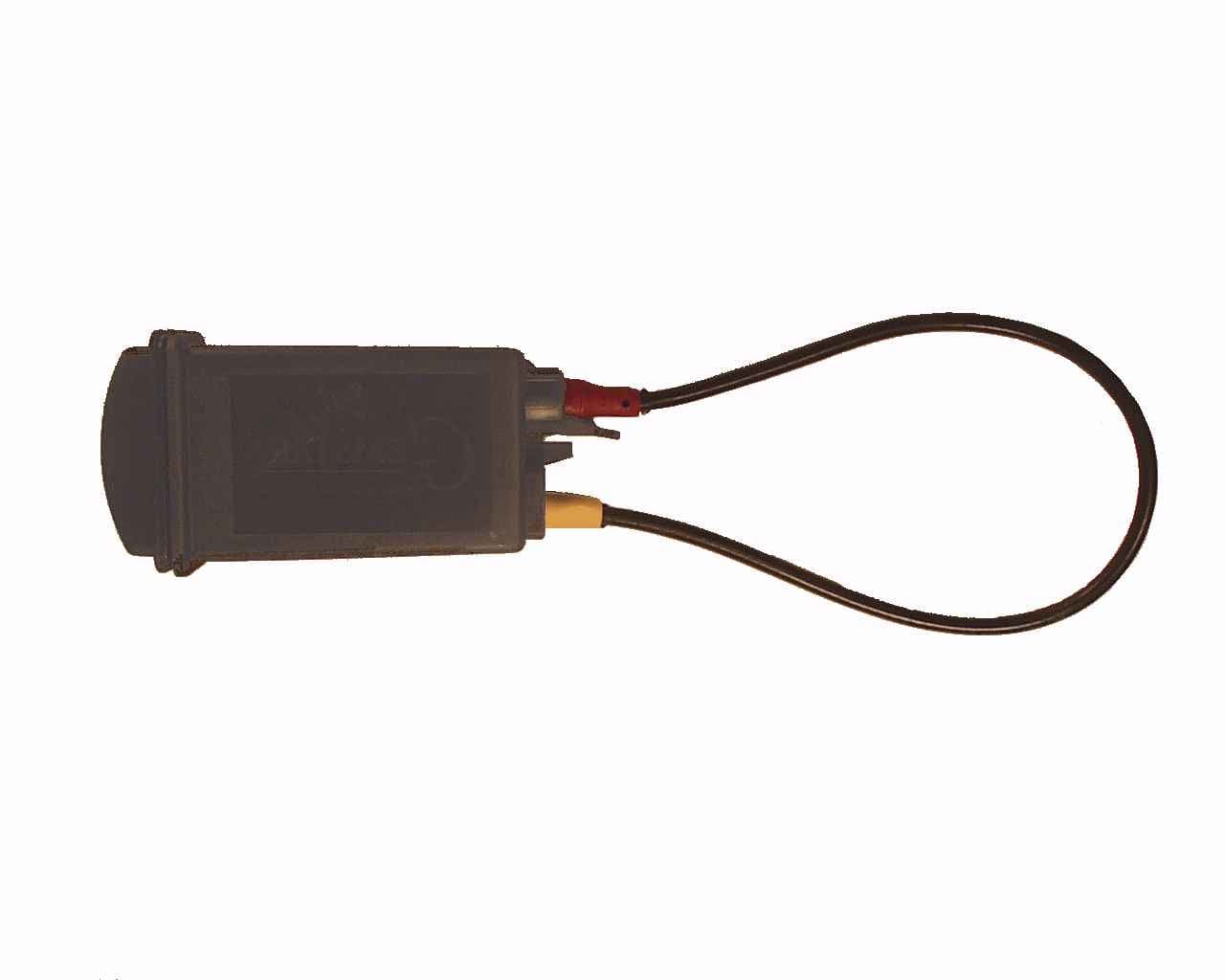
N6OGSAMATB01
Nov 15, 1998Automated Inventory Control System (AICS) Asset Ta
Equipment Class
DXX - Part 15 Low Power Communication Device Transmitter