NK4-7039795714
io Wave Inc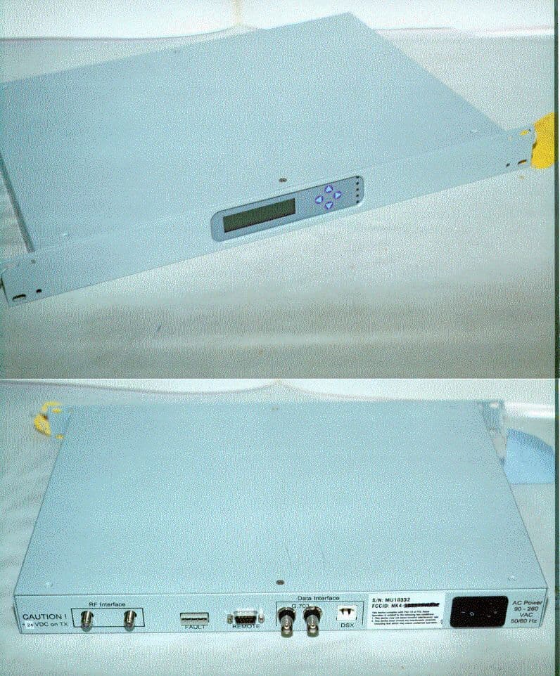
Click to zoom
Application Details
- Equipment Class
- DSS - Part 15 Spread Spectrum Transmitter
- Date of Grant
- Oct 06, 1999
- Application Purpose
- Original Equipment
- Date of Application
- Jul 24, 1999
- Frequency Range
- 2412.00000000 - 2470.00000000
- Company
- io Wave Inc
- Country
- United States
Documents & Files
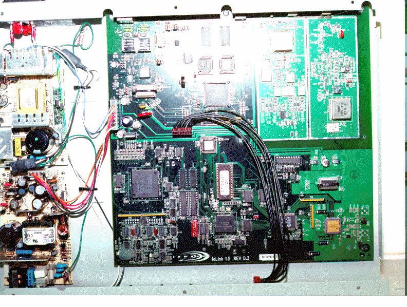
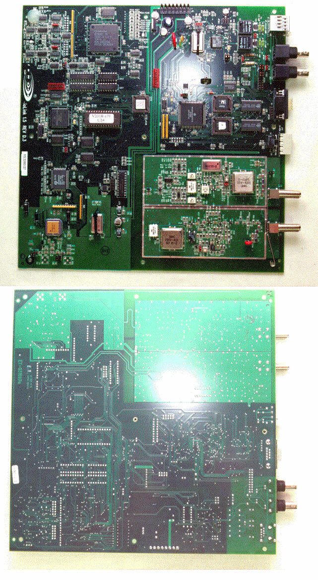
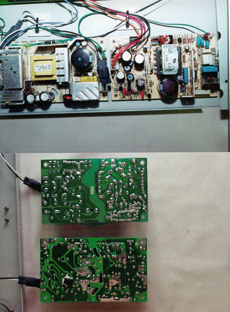
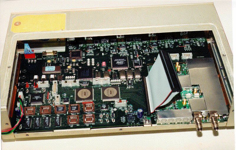
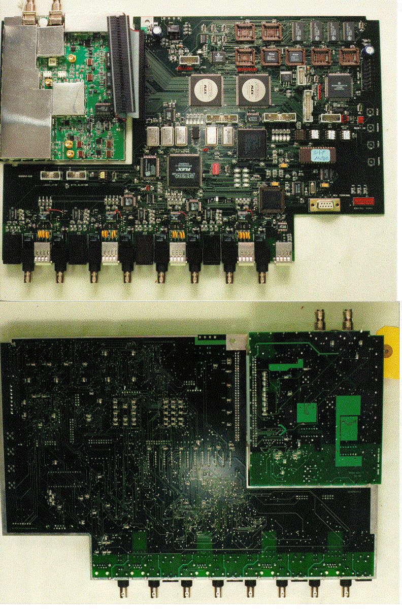
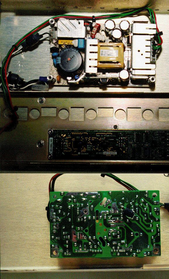
Document Text
Text extracted from the exhibit documents filed with the FCC. Open a document above to read the original.
Users Manual
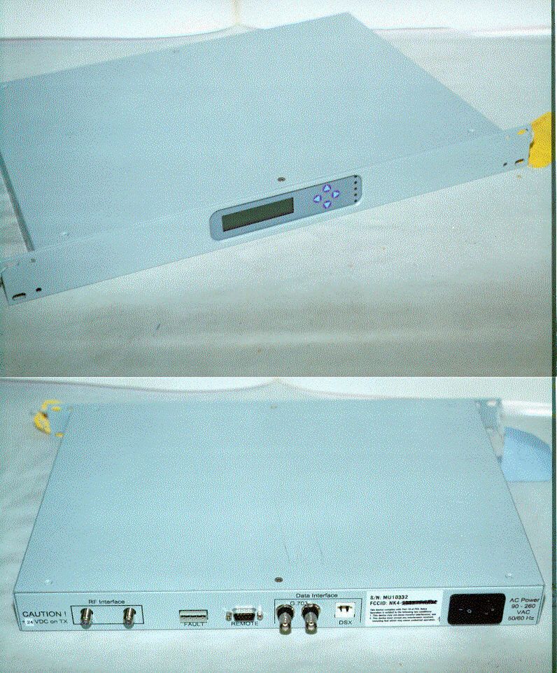
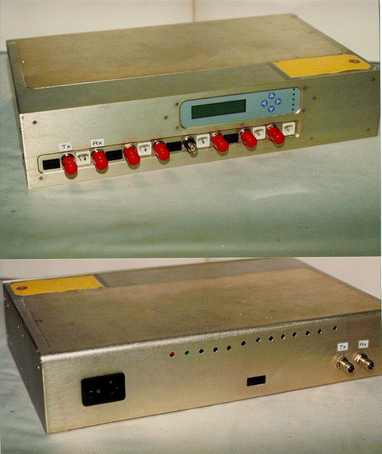
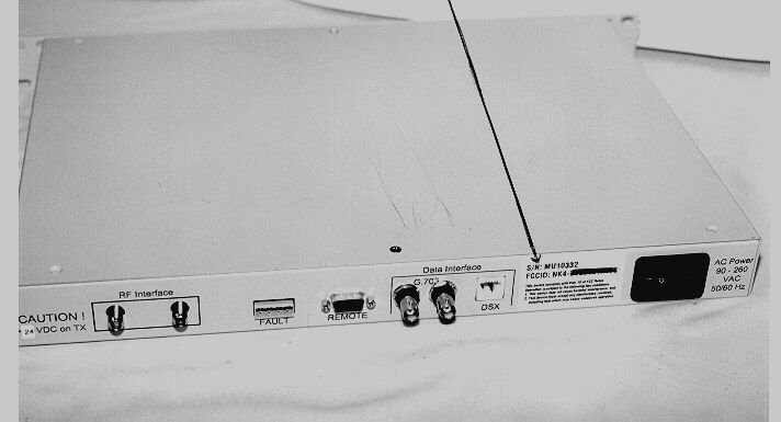
02/99 PRELIMINARY . User Guide Technical Reference for ioLink 4 Wireless System 1010 Wisconsin Avenue • NW • Suite 250 • Washington, DC 20007 Telephone: (202) 333-9283 • Facsimile: (202) 333-0984 • http://www.iowave.com Pwr TX RX RF Alm ioLink 4 CONSOLE TX RX 1 TX RX 2 TX RX 3 TX RX 4 02/99 PRELIMINARY Welcome We welcome you to the world of Wireless Communications. To familiarize you with the ioLink 4 and help you get the most out of the system, please review the enclosed information and keep it for your reference. You will find: 1. Quick Start Installation Guide booklet to provide you with an overview of the system, installation instructions, and troubleshooting tips. 2. This User Technical Reference Guide that contains in depth information on how to use the system. It is designed for system managers, telecommunications engineers and electrical engineers those involved in hands on operation, troubleshooting, and monitoring of communications systems. Please be sure to read the section entitled “Important Information Regarding Your ioLink 4 Wireless System” which appears in Appendix C. We value your investment in our system and encourage you to call us with your comments and suggestions. We look forward to serving you. Copyright 1999 by ioWave, Inc. All rights reserved. No part of this manual may be reproduced without express written consent from ioWave. The information contained in this manual is subject to change without notice. PRELIMINARY Customer Support (202) 333-7031 ii Welcomei Table of Contentsii Table of Figuresiv Table of Tables v SECTION 1 ioLink 4 PRODUCT DESCRIPTION1-1 1.1 Key Features and Benefits1-1 1.2 Advanced Features1-2 1.2.1 Performance Monitoring1-2 1.2.2 Forward Error Correction Alert 1-3 1.3 How to Contact Us1-3 SECTION 2 ioLink 4 SYSTEM COMPONENTS2-1 2.1 Modem (Indoor) Unit Description2-1 2.2 Intermediate Frequency Cable2-2 2.3 RF (Outdoor) Unit Description2-3 2.4 Radio Frequency Cable2-4 2.5 Antenna Description2-5 2.6 Antenna Selection and Consideration2-5 2.6.1 Size2-5 2.6.2 Polarization2-6 2.7 Typical Link Setup2-7 2.7.1 Normal Operation2-8 2.7.2 LCD Screen Cycling2-8 2.8 Advanced Features2-8 2.8.1 Performance Monitoring2-9 2.8.2 Forward Error Correction 2-9 2.8.3 Diagnostic Testing 2-13 SECTION 3 OPERATING THE ioLink 43-1 3.1 Front Panel Interactions3-1 3.1.1 LED Indicators3-2 3.1.2 Keypad and LCD3-2 3.1.3 ioLink 4 LCD Menus3-3 3.1.3.1 STATUS Menu Item Descriptions3-4 3.1.3.2 CONFIGURATION Menu Item Descriptions3-5 3.1.3.3 TEST Menu Item Descriptions3-6 3.1.3.4 ALARM Menu Item Descriptions3-8 3.1.3.5 ADVANCED Menu Item Descriptions 3-10 3.1.4 Remote Control (CONSOLE) Connection 3-12 3.1.5 E1/G.703 Interface 3-12 3.1.6 T1 Interface 3-13 3.1.7 Pin Outs for Front Panel Connectors 3-13 Table of Contents Table of Contents PRELIMINARY Customer Support (202) 333-7031 iii Continued 3.2 Rear Panel Interactions 3-14 3.2.1 Power Connector 3-14 3.2.2 Alarm Fault Connector 3-15 3.2.3 RF Interface Connectors 3-15 3.2.4 Pin Outs for Rear Panel Alarm Terminal Block 3-15 SECTION 4 NETWORK MANAGEMENT FOR ioLink 44-1 4.1 Functionality4-1 4.2 Configuration4-2 4.3 Test Modes4-3 4.4 Performance Monitoring 4-4 4.5 Error/Alarm Monitoring4-5 4.5.1 Near-end Related Alarms4-5 4.5.2 RF or Far-end Related Alarms4-5 SECTION 5 TROUBLESHOOTING ALARM CONDITIONS FOR ioLink 45-1 5.1 Transmit LOS5-1 5.2 LIU Not Responding 5-1 5.3 Firmware Not Responding5-1 5.4 FEC BER > x.x E-x5-2 5.5 FEC Decoder Not Locked5-2 5.6 RX Low Signal Power5-3 5.7 RX Low Symbol Power5-3 5.8 No Acquisition5-5 5.9 Alarm Indication System (AIS)5-5 APPENDIX A TECHNICAL SPECIFICATIONS FOR ioLink 4A-1 APPENDIX B GLOSSARY OF TERMSB-1 APPENDIX C IMPORTANT INFORMATION ABOUT YOUR SYSTEMC-1 C.1 FCC Regulatory NoticeC-1 C.2 WarrantyC-1 C.3 DisclaimerC-3 C.4 Use of ioWave Products Outside of the United StatesC-3 PRELIMINARY Customer Support (202) 333-7031 iv Figure 1-1. Typical Link Setup1-2 Figure 2-1. Modem Unit Front Panel 2-1 Figure 2-2. Modem Unit Rear Panel 2-1 Figure 2-3. RF Unit Connections2-3 Figure 2-4. RF Unit Block Diagram2-4 Figure 2-5. Typical Link Diagram2-5 Figure 2-6. LCD Screen Cycling2-8 Figure 2-7. Forward Error Correction (FEC) Improvement of Bit Error Rate (BER) for Differential Quadrature Phase Shift Keying (DQPSK)2-12 Figure 3-1. Modem Unit Front Panel 3-1 Figure 3-2. Full Loopback3-6 Figure 3-3. Far-end Loopback3-3 Figure 3-4. Source Loopback3-4 Figure 3-5. FEC Loopback3-11 Figure 3-6. LIU Loopback (Local)3-11 Figure 3-7. LIU Loopback (Remote)3-12 Figure 3-8. DSX-1 (RJ-48C – female) Pin Assignments3-13 Figure 3-9. Modem Unit Back Panel 3-14 Figure 3-10. Terminal Block (Form-C contacts) Pin Assignments3-15 Figure 5-1. Received Signal Strength Indicator (RSSI) Voltage Conversion5-4 Table of Figures PRELIMINARY Customer Support (202) 333-7031 v Table 3-1. Light Emitting Diode (LED) Indicators3-2 Table 3-2. Liquid Crystal Display (LCD) Menu Defaults3-3 Table 3-3. Status Menu Items3-4 Table 3-4. Configuration Menu Parameters3-5 Table 3-5. Alarm Menu Conditions3-8 Table 3-6. Advanced Menu Options3-10 Table A-1. Technical Specifications for ioLink 4A-1 Table of Tables PRELIMINARY Customer Support (202) 333-70311-1 The ioLink 4 provides four full-duplex Direct Sequence Spread Spectrum (DSSS) devices for T1/E1 rate wireless communications between two line of sight (LOS) locations. It can be connected to many types of interfaces to meet various communication needs. The technologies incorporated in the ioLink 4 give you an efficient, minimal interference, error-resistant link compare to other services, and a superior carrier-to- interference (C/I) performance ratio. 1.1 Key Features and Benefits The ioLink 4 system provides many important features and benefits: • Offers quick turnaround on investment and savings versus recurring leased line charges • Does not require user licensing (complies with FCC regulation Part 15) • Provides clear and robust communications over a range of distances • Is capable of voice, video…
Text truncated - open the document above for the full version.
Users Manual
02/99 PRELIMINARY . User Guide Technical Reference for ioLink 4 Wireless System 1010 Wisconsin Avenue • NW • Suite 250 • Washington, DC 20007 Telephone: (202) 333-9283 • Facsimile: (202) 333-0984 • http://www.iowave.com Pwr TX RX RF Alm ioLink 4 CONSOLE TX RX 1 TX RX 2 TX RX 3 TX RX 4 02/99 PRELIMINARY Welcome We welcome you to the world of Wireless Communications. To familiarize you with the ioLink 4 and help you get the most out of the system, please review the enclosed information and keep it for your reference. You will find: 1. Quick Start Installation Guide booklet to provide you with an overview of the system, installation instructions, and troubleshooting tips. 2. This User Technical Reference Guide that contains in depth information on how to use the system. It is designed for system managers, telecommunications engineers and electrical engineers those involved in hands on operation, troubleshooting, and monitoring of communications systems. Please be sure to read the section entitled “Important Information Regarding Your ioLink 4 Wireless System” which appears in Appendix C. We value your investment in our system and encourage you to call us with your comments and suggestions. We look forward to serving you. Copyright 1999 by ioWave, Inc. All rights reserved. No part of this manual may be reproduced without express written consent from ioWave. The information contained in this manual is subject to change without notice. PRELIMINARY Customer Support (202) 333-7031 ii Welcomei Table of Contentsii Table of Figuresiv Table of Tables v SECTION 1 ioLink 4 PRODUCT DESCRIPTION1-1 1.1 Key Features and Benefits1-1 1.2 Advanced Features1-2 1.2.1 Performance Monitoring1-2 1.2.2 Forward Error Correction Alert 1-3 1.3 How to Contact Us1-3 SECTION 2 ioLink 4 SYSTEM COMPONENTS2-1 2.1 Modem (Indoor) Unit Description2-1 2.2 Intermediate Frequency Cable2-2 2.3 RF (Outdoor) Unit Description2-3 2.4 Radio Frequency Cable2-4 2.5 Antenna Description2-5 2.6 Antenna Selection and Consideration2-5 2.6.1 Size2-5 2.6.2 Polarization2-6 2.7 Typical Link Setup2-7 2.7.1 Normal Operation2-8 2.7.2 LCD Screen Cycling2-8 2.8 Advanced Features2-8 2.8.1 Performance Monitoring2-9 2.8.2 Forward Error Correction 2-9 2.8.3 Diagnostic Testing 2-13 SECTION 3 OPERATING THE ioLink 43-1 3.1 Front Panel Interactions3-1 3.1.1 LED Indicators3-2 3.1.2 Keypad and LCD3-2 3.1.3 ioLink 4 LCD Menus3-3 3.1.3.1 STATUS Menu Item Descriptions3-4 3.1.3.2 CONFIGURATION Menu Item Descriptions3-5 3.1.3.3 TEST Menu Item Descriptions3-6 3.1.3.4 ALARM Menu Item Descriptions3-8 3.1.3.5 ADVANCED Menu Item Descriptions 3-10 3.1.4 Remote Control (CONSOLE) Connection 3-12 3.1.5 E1/G.703 Interface 3-12 3.1.6 T1 Interface 3-13 3.1.7 Pin Outs for Front Panel Connectors 3-13 Table of Contents Table of Contents PRELIMINARY Customer Support (202) 333-7031 iii Continued 3.2 Rear Panel Interactions 3-14 3.2.1 Power Connector 3-14 3.2.2 Alarm Fault Connector 3-15 3.2.3 RF Interface Connectors 3-15 3.2.4 Pin Outs for Rear Panel Alarm Terminal Block 3-15 SECTION 4 NETWORK MANAGEMENT FOR ioLink 44-1 4.1 Functionality4-1 4.2 Configuration4-2 4.3 Test Modes4-3 4.4 Performance Monitoring 4-4 4.5 Error/Alarm Monitoring4-5 4.5.1 Near-end Related Alarms4-5 4.5.2 RF or Far-end Related Alarms4-5 SECTION 5 TROUBLESHOOTING ALARM CONDITIONS FOR ioLink 45-1 5.1 Transmit LOS5-1 5.2 LIU Not Responding 5-1 5.3 Firmware Not Responding5-1 5.4 FEC BER > x.x E-x5-2 5.5 FEC Decoder Not Locked5-2 5.6 RX Low Signal Power5-3 5.7 RX Low Symbol Power5-3 5.8 No Acquisition5-5 5.9 Alarm Indication System (AIS)5-5 APPENDIX A TECHNICAL SPECIFICATIONS FOR ioLink 4A-1 APPENDIX B GLOSSARY OF TERMSB-1 APPENDIX C IMPORTANT INFORMATION ABOUT YOUR SYSTEMC-1 C.1 FCC Regulatory NoticeC-1 C.2 WarrantyC-1 C.3 DisclaimerC-3 C.4 Use of ioWave Products Outside of the United StatesC-3 PRELIMINARY Customer Support (202) 333-7031 iv Figure 1-1. Typical Link Setup1-2 Figure 2-1. Modem Unit Front Panel 2-1 Figure 2-2. Modem Unit Rear Panel 2-1 Figure 2-3. RF Unit Connections2-3 Figure 2-4. RF Unit Block Diagram2-4 Figure 2-5. Typical Link Diagram2-5 Figure 2-6. LCD Screen Cycling2-8 Figure 2-7. Forward Error Correction (FEC) Improvement of Bit Error Rate (BER) for Differential Quadrature Phase Shift Keying (DQPSK)2-12 Figure 3-1. Modem Unit Front Panel 3-1 Figure 3-2. Full Loopback3-6 Figure 3-3. Far-end Loopback3-3 Figure 3-4. Source Loopback3-4 Figure 3-5. FEC Loopback3-11 Figure 3-6. LIU Loopback (Local)3-11 Figure 3-7. LIU Loopback (Remote)3-12 Figure 3-8. DSX-1 (RJ-48C – female) Pin Assignments3-13 Figure 3-9. Modem Unit Back Panel 3-14 Figure 3-10. Terminal Block (Form-C contacts) Pin Assignments3-15 Figure 5-1. Received Signal Strength Indicator (RSSI) Voltage Conversion5-4 Table of Figures PRELIMINARY Customer Support (202) 333-7031 v Table 3-1. Light Emitting Diode (LED) Indicators3-2 Table 3-2. Liquid Crystal Display (LCD) Menu Defaults3-3 Table 3-3. Status Menu Items3-4 Table 3-4. Configuration Menu Parameters3-5 Table 3-5. Alarm Menu Conditions3-8 Table 3-6. Advanced Menu Options3-10 Table A-1. Technical Specifications for ioLink 4A-1 Table of Tables PRELIMINARY Customer Support (202) 333-70311-1 The ioLink 4 provides four full-duplex Direct Sequence Spread Spectrum (DSSS) devices for T1/E1 rate wireless communications between two line of sight (LOS) locations. It can be connected to many types of interfaces to meet various communication needs. The technologies incorporated in the ioLink 4 give you an efficient, minimal interference, error-resistant link compare to other services, and a superior carrier-to- interference (C/I) performance ratio. 1.1 Key Features and Benefits The ioLink 4 system provides many important features and benefits: • Offers quick turnaround on investment and savings versus recurring leased line charges • Does not require user licensing (complies with FCC regulation Part 15) • Provides clear and robust communications over a range of distances • Is capable of voice, video…
Text truncated - open the document above for the full version.
Cover Letter(s)
June 15, 1999 Federal Communications Commission 7435 Oakland Mills Road Columbia, MD 21046 ATTN: Applications Examining Division RE: io Wave, Inc., Certification Application; FCCID: NK4-7039795714 Gentlemen: Please find the enclosed application for Certification of a Part 15 Direct Sequence Spread Spectrum Transmitter. TheModel 2.4 GHz ioLink4/ioLink1 Wireless Systemwill interface with a terminal via RS-232 port, and therefore may be considered a Class A Digital Device as well. Class A is justifiable since the system is intended for, and marketed only to commercial operators. The system has high quality with fast T1 data through-put, as well as being priced way over any consumer product. Commercial applications are outlined in the User Manual. The 56 cm minimum safe distance limit for 1 mW/cm RF exposure, as shown in the User ManualAppendix C1,was calculated fromFCC OET 65 Appendix B, Table 1Bguidlines for General Population/Uncontrolled Exposure. This calculation was based on the highest EIRP possible from the system, considering maximum power and antenna gain. The formula used was: S = (Po*G)/(4*pi*r^2) The RF unit incorporates a standard N connector to the antenna, therefore requiring professional installation. Appendix C of the User Manual specifies that only trained ioWave certified technicians should install theioLink4/1. There are many technical steps needed to install an operating full-duplex system, as outlined in the manual. These include antenna support structure, site survey, antenna alignment, test and troubleshoot. All systems sold to businesses are installed by io Wave, Inc. Marketing is limited sales by authorized dealers. Your consideration is much appreciated. Sincerely, Steven Dayhoff Chief Engineer
Operational Description
Theory of Operation. The iolink 1 is a full-duplex Tl rate radio operating in the 2.4 GHz ISM band. The data transmitted through the iolink 1 is processed in the following sequence: LIU <-> FEC <-> Baseband (DSSS) <-> IF <-> RF ------ RF <-> IF <-> Baseband <-> FEC <-> LIU Below, TX indicates the data stream toward the antenna and RX indicates the data stream from the antenna. Line Interface Unit TX: The LIU converts the tip and ring input from the external device to clock and data (RCLK and RPOS) which are passed to the FEC. The data from the connections, RJ-48 and BNC, pass through a transformer, fuses, lightning protection and voltage limiting diodes on the input lines. RX: The data received from the link is converted to tip and ring. The data to the output connections, RJ48 and BNC, pass through a transformer, fuses, lightning protection and voltage limiting diodes on the output lines. Forward Error Correction TX: RCLK and RPOS pass from the LIU to the FEC ASIC. The data is encoded using Rate 3/4 punctured convolutional coding which increases the data rate from Tl (1.544 Mbps) to 4/3 Tl (2.059 Mbps). The data is passed to the Spread Spectrum ASIC. RX: The received data from the DSSS ASIC is decoded using a Viterbi decoder. Baseband TX: The baseband processing is performed by a Spread Spectrum ASIC and an A/D. The data bits from the FEC (encoded RPOS) are processed as pairs of bits, one bit for the in-phase channel (1) and one for the quadrature channel (Q); thus, two bits make one QPSK symbol and the symbol rate is half the encoded data rate. The QPSK symbols are then processed sequentially by the differential encoder, the PN code modulator and the QPSK modulator. The result is a digitized IF signal which has been spread by the PN code modulator. A 10 chiptsymbol PN code is used. The I and Q channels for the symbols are passed to the IF section. RX: The received signals from the IF section, RXI and RXQ, are first processed by the AID which samples at a rate equal to the data rate * code length * 2 = 41.173 MHz. The digitized signal is then passed to the Spread Spectrum ASIC and processed by the digital downconverter which converts it to baseband. This is followed by the matched filter which samples I and Q twice per chip to compute the cross-correlation and then the symbol tracking processor which detects the optimal de-spread I and Q symbols. The de-spread I and 0 symbols are sent to the differential demodulator, where the current and previous symbols are processed in order to identify the encoded bits. The bits are processed by the output data processor to produce a serial bit stream which is transmitted to the FEC on RXOUT. lntermediate Frequency TX: The symbols from the Baseband are sent to the IF section as TXI and TXQ. These are mixed with a 1 1 0 MHz oscillator (with a 90 degree phase difference for I and Q) to bring them up to the IF frequency. Then, I and Q are summed and the resultant signal is passed through an AGC and filter (25 MHz bandpass) befbre being sent to the RF unit for upconverting to the 2.4 GHz transmission frequency. RX: The down-converted 70 MHz signal is passed through an AGC and bandpass filter, then decomposed into I and Q. The analog symbols, RXI and RXQ, are passed through the A/D as described above. Radio Frequency Unit TX: The llO MHz IF signal is passed through an AGC circuit, then up-converted to 2.4GHz.This is then amplified to +25 dBm and passed through a filter to the antenna. RX: The signal received from the antenna is passed through an AGC circuit, then down-converted to 70 MHz and filtered before being passed to the IF cable.
RF Exposure Info
RF Exposure Calculations: The following information provides the minimum seperation distance for the dish antenna provided with the ioLink4/1 system, as calculated fromFCC OET 65 Appendix B, Table 1BGuidlines for General Population/Uncontrolled Exposure. This calculation is based on the highest EIRP possible from the system, considering maximum power and antenna gain. The formula used was: S = (Po*G)/(4*pi*r^2) Where S = 1.0 mW/cm^2 for 2400 MHz. Where Po = 315 mW max. For: 21 dB Dish Antenna - Comsat Model P-24A24N ......r = 56 cm The following statement will be presented in the ioLink4/1 User Manual, Appendix C1: WARNING In order to comply with the FCC adopted RF exposure requirements, this transmitter system will be installed by the manufacturer's resaler professional. Installation of the 2 ft. parabolic dish antenna must be performed in a manner that will provide at least 56 cm clearance from the front side of the dish, to any personnel such as employee or member of the public.
Schematics
A A B B C C D D E E 44 33 22 11 420-470039D 2.4 RF UNIT PS -- MCU_DTMF ioWave Inc. 1010 Wisconsin Ave. NW Suite 215 Washington, D.C. 20007 202.333.9283 (0984 fax) @1997 C 23Wednesday, June 16, 1999 Title SizeDocument NumberRev Date:Sheet of TX_VSWR_IN RB0 RB1 RB2 RB3 RB4 RB5 RB6 RB7 RB7 RB6 RB5 RB4 RB0 RB2 RB1 RB3 RB[7..0] RC0 RC0 SDO SDI SPI_CS SCK TX RX RSSI_IN 24_IN 15_IN 6_IN VCC VCC2 VCC2 VCC2 VCC2 VCC2 VCC2 VCC2 VCC2 VCC2 VCC2 VCC2 VCC2 VCC2 VCC2 +7VA +7VA +7VA +7VA VCC2 C24 .01UF 1 2 C27 0.1UF 1 2 C26 0.1UF 1 2 C18 0.1UF 1 2 C30 0.1UF 1 2 C29 0.1UF 1 2 C22 0.1UF 12 C17 0.1UF 1 2 C25 0.1UF 1 2 C15 0.1UF 1 2 C20 0.1UF 1 2 C32 0.1UF 1 2 C31 0.1UF 1 2 C23 0.47UF C16 20PF 12 C19 20PF 12 D8 BAV99 3 1 2 D7 BAV99 3 1 2 D6 BAV99 3 1 2 D5 BAV99 3 1 2 D9 BAV99 3 1 2 Y1 XTAL 3.579MHZ 1 2 JP5 HEADER 8_L 1 2 3 4 5 6 7 8 1 2 3 4 5 6 7 8 L8 1uH 12 L10 1uH 12 + - U9B MC33072 5 6 7 8 4 + - U9A MC33072 3 2 1 8 4 U7 MT8880CS 1 2 3 4 19 18 20 14 15 16 17 9 10 5 6 7 8 11 12 13 IN+ IN- GS VREF ST EST VDD D0 D1 D2 D3 R/W CS VSS OSC1 OSC2 TONE RS0 CLK /IRQ R50 0 12 R39 0 12 R52 DNI 1 2 R49 DNI 1 2 R42 DNI 1 2 R40 0 12 R38 DNI 1 2 R43 DNI 1 2 R32 100 12 R30 100 12 R21 100 12 R24 100 12 R28 100 12 R37 100K 12 R35 100K 12 R22 10K 1 2 R25 10K 1 2 R29 10K 1 2 R31 10K 1 2 R33 10K 1 2 R41 10K 1 2 R48 10K 12 R54 10K 12 R44 10K 1 2 R55 10K 1 2 R53 10K 12 R51 10K 12 R47 10K 1 2 R46 1K 12 R20 2.0K 12 R23 20K_5% 12 R26 20K_5% 12 R27 20K_5% 12 R34 374K 1% 12 R45 4K 12 XU6 SOCKET_28_TH_300 U6 PIC16C76 1 2 3 4 5 6 7 8 9 10 11 12 13 14 15 16 17 18 19 20 21 22 23 24 25 26 27 28 MCLR/Vpp RA0/AN0 RA1/AN1 RA2/AN2/VREF RA3/AN3 RA4/TOCKI RA5/AN4/SS Vss OSC1/CLKIN OSC2/CLKOUT RC0/T1OSO/T1CKI RC1/T1OSI/CCP2 RC2/CCP1 RC3/SCK/SCL RC4/SDI/SDA RC5/SDO RC6/TX/CK RC7/RX/DT Vss VDD RB0/INT RB1 RB2 RB3 RB4 RB5 RB6 RB7 R36 750 + - U8 MC33071 3 2 6 71 45 L11 1uH 12 VCC GND TX_VSWR_LEV RCV_LEV DTMF 6V 15V 24V +7.5V
Schematics
A A B B C C D D E E 44 33 22 11 REGULATOR HARDWARE BOARD MTG HARDWARE TOOLING HOLES 420-4700039D 2.4 RF UNIT PS - MECH_PARTS ioWave Inc. 1010 Wisconsin Ave. NW Suite 215 Washington, D.C. 20007 202.333.9283 (0984 fax) @1997 B 33Monday, June 28, 1999 Title SizeDocument NumberRev Date:Sheet of 4SCREW1SCREW_4 NUT1NUT4 4SCREW2SCREW_4 4SCREW3SCREW_4 NUT2NUT4 NUT3NUT4 X2 MTGHOLES _TRIDIEPLEXER J13 MTG 1 J15 MTG 1 J5 MTG 1 J12 MTG 1 J14 MTG 1 J6 MTG125 1 J9 MTG125 1 J11 MTG125 1 FID1 FIDUCIAL 1 FID2 FIDUCIAL 1 FID3 FIDUCIAL 1 J16 MTG125 1 GND
Schematics
A A B B C C D D E E 44 33 22 11 REMOVE JP4 SHUNT IF POWER SUPPLY IS GREATER THAN 30V POWER SUPPLY TO TXCVR BOARD MECHANICAL PARTS AND ADDITIONAL VIAS MICROCONTROLLER A/D CHANNELS DTMF TXCVR POWER SUPPLY TO POWER AMPLIFIER BOARD 70 MHZ IF FROM RF TXCVR BOARD 70 MHZ IF TO ODU CHASSIS BULKHEAD +6V +6V Gnd 420-4700039D 2.4 RF UNIT POWER SUPPLY -- TOP LEVEL ioWave Inc. 1010 Wisconsin Ave. NW Suite 215 Washington, D.C. 20007 202.333.9283 (0984 fax) @1997 C 13Monday, June 21, 1999 Title SizeDocument NumberRev Date:Sheet of MECH1 MECH_PARTS GND MCU MCU_DTMF VCC GND TX_VSWR_LEV RCV_LEV DTMF 24V 15V 6V +7.5V RCV_LEV TX_VSWR_LEV DTMF+RSSI +24V +7.5V +6.0V +5V +24V +7.5V +7.5V +6.0V +15V +15V +7.5V +5V C12 .01UF 12 C14 .01UF 12 C13 100PF 1 2 C2 0.1UF 1 2 C11 0.1UF 1 2 + C4 1000UF 25V + C3 100UF 50V + C1 100UF 50V + C5 100UF 50V + C6 100UF 50V + C7 10UF 35V + C10 10UF 35V D1 DIODE_1N5822_TH D2 1N4744A 2 1 JP4 HEADER 2X1_TH_L 1 2 1 2 JP1 HEADER 2X1_TH_L 1 2 1 2 L1 100UH 12 L3 1uH 12 L4 1uH 12 L5 1uH 1 2 L2 21.65 UH 12 + - U5 MC33071 3 2 6 71 45 R19 DNI 12 R9 0 1 2 R56 0 12 R18 100K 1 2 R3 10K 12 R4 1K 1 2 R7 1K 1 2 R5 2.4K 1 2 R15 2.7K 12 R17 2.7K 12 R13 24 12 R8 3.9K 5% 1 2 R11 330 2W 1 2 R1 5.6K 5% 1 2 R16 680 12 R12 910 1 2 R14 1K POT 13 2 R2 1K POT 1 3 2 R10 1K POT 1 3 2 R6 1K POT 1 3 2 X1 SHUNT JP2 HEADER 3L 1 2 3 1 2 3 JP3 HEADER 10L 1 2 3 4 5 6 7 8 9 10 1 2 3 4 5 6 7 8 9 10 J3 SMA 1 2345 L6 220nH 1 2 C9 120PF 12 C8 120PF 12 D3 1N4744A 2 1 D4 SMS7630 21 J1 MCX 1 2345 J2 MCX 1 2345 U3 LM2941T 12 3 45 6 ADJON/OFF GND INOUT TAB U2 LM2941T 12 3 45 6 ADJON/OFF GND INOUT TAB U4 LM341T-15 13 24 INOUT GNDTAB U1 LM2576HV 12 3 4 56 VinOutput GND FB ON/OFFTAB
Schematics
IoWave Proprietary - 1 - 470045-000 A IOLINK4 IF SECTION - TOP PAGE ioWave Inc.1010 Wisconsin Ave. NW Suite 215Washington, D.C. 20007202.333.9283 (0984 fax)@1997 C 16 Thursday, February 18, 1999 TitleSize Document Number Rev Date: Sheet of ADC1ADC Q[7..0]I[7..0] DGND AGND VCC Q_IN I_IN CLK_IN VCCIO DAC1DAC CLK VCC DGND AGND C_OUT Y_OUT D O C[13..0] Y[13..0] VCCIO PS1POWER12 AGND +12V +24V TX1MOD I_IN Q_IN +12V AGND TX_OUT +24V RX1DEMOD +12V AGND RX_IN I_OUTQ_OUT RCV_LOBAND AGC VCC VCC VCC VCC VCCIO VCCIO VCCIO VCCIO VRF+ VRF+ VRF+ VRF++12V+12V +12V RCV_IRCV_Q AGC_VTX_ITX_Q RCV_LOBAND RX_IN TX_OUT RCV_CLK RCVQ_1RCVQ_3RCVQ_5RCVQ_7 RCVQ_0RCVQ_2RCVQ_4RCVQ_6 RCVI_1RCVI_3RCVI_5RCVI_7 RCVI_0RCVI_2RCVI_4RCVI_6 RCVQ_[7..0] RCVI_[7..0] TxCLK XMTI_12XMTI_10XMTI_8XMTI_6XMTI_4XMTI_2XMTI_0 XMTI_13XMTI_11XMTI_9XMTI_7XMTI_5XMTI_3XMTI_1 XMTQ_12XMTQ_10XMTQ_8XMTQ_6XMTQ_4XMTQ_2XMTQ_0 XMTQ_13XMTQ_11XMTQ_9XMTQ_7XMTQ_3XMTQ_1XMTQ_5 XMTQ_[13..0]XMTI_[13..0]AGC_1_OUT M1XXX1M2XXX1 Z_PCB1IO4_IF PCB J1 TNC 2 1 3 4 J2 TNC 2 1 3 4 JP1HEADER 36X2TSW-136-08-G-D-RA 1 2 3 4 5 6 7 8 9 10 11 12 13 14 15 16 17 18 19 20 21 22 23 24 25 26 27 28 29 30 31 32 33 34 35 36 37 38 39 40 41 42 43 44 45 46 47 48 49 50 51 52 53 54 55 56 57 58 59 60 61 62 63 64 65 66 67 68 69 70 71 72 1234567891011 12 13 14 15 16 17 18 19 20 21 22 23 24 25 26 27 28 29 30 31 32 33 34 35 36 37 38 39 40 41 42 43 44 45 46 47 48 49 50 51 52 53 54 55 56 57 58 59 60 61 62 63 64 65 66 67 68 69 70 71 72 TIE ANALOG and DIGITAL GROUNDS TOGETHER AT SINGLE POINT IoWave Proprietary - 2 - 470045-000 A A_to_D CONVERTER ioWave Inc.1010 Wisconsin Ave. NW Suite 215Washington, D.C. 20007202.333.9283 (0984 fax)@1997 C 26 Thursday, February 18, 1999 TitleSize Document Number Rev Date: Sheet of VADC1VADC2 VADC1 VDRVVDRV VADC2 VADC3VADC3 VREFTIVREFBI VREFTQ VREFBQ VREFTI VCC +5V VADC1 VDRV VREFBI VREFBQVREFTQ VCCIO VCCIOVCCIO VCCIO VADC2VADC3 VCCDGND GND AGND ID7ID6ID5ID4ID3ID2ID1ID0QD7QD6QD5QD4QD3QD2QD1QD0 ID0ID1ID2ID3ID4ID5ID6ID7QD0QD1QD2QD3QD4QD5QD6QD7 QD[7..0]ID[7..0] I0I1I2I3I4I5I6I7Q0Q1Q2Q3Q4Q5Q6Q7 I[7..0]Q[7..0] QD7 QD6 QD5 QD4 QD3 QD2 QD1 QD0 ID7 ID6 ID5 ID4 ID3 ID2 ID1 ID0 TP9TestPOINT 1 TP10TestPOINT 1 TP20TestPOINT 1 TP22TestPOINT 1 TP23TestPOINT 1 TP24TestPOINT 1 TP19TestPOINT 1 TP21TestPOINT 1 TP11TestPOINT 1 TP12TestPOINT 1 TP13TestPOINT 1 TP14TestPOINT 1 TP15TestPOINT 1 TP16TestPOINT 1 TP17TestPOINT 1 TP18TestPOINT 1 TP1TestPOINT 1 TP2TestPOINT 1 TP3TestPOINT 1 TP4TestPOINT 1 TP5TestPOINT 1 TP6TestPOINT 1 TP7TestPOINT 1 TP8TestPOINT 1 R117270 12 R118150 12 C2.01UF 12 C18.01UF 12 C21.01UF 12 C35.01UF 12 C6.01UF 12 C120.1uF 12 C130.1uF 12 C100.1uF 12 C270.1uF 12 C290.1uF 12 C300.1uF 12 C370.1uF 12 C390.1uF 12 C240.1uF 12 C50.1uF 12 C81UF 1 2 C141UF 1 2 C251UF 1 2 C311UF 1 2 C927PF 12 C2627PF 12 R110 1 2 R10 1 2 R200 1 2 R220 1 2 R250 1 2 R270 1 2 R24102K1% 1 2 R29107K1% 1 2 R28174K 1% 12 R1439 1 2 R539 1 2 R239 1 2 R639 1 2 R1539 1 2 R1651 12 R751 12 R2371.5K 1% 12 R3OMIT 1 2 R13OMIT 1 2 U4ADS830 10234567891 11121314151617181920 CLK B1B2B3B4B5B6B7B8 GND RSELINT/EXT REFBREFTCMININGND+VSVDRV U1ADS830 10234567891 11121314151617181920 CLK B1B2B3B4B5B6B7B8 GND RSELINT/EXT REFBREFTCMININGND+VSVDRV U6 LM385 48 5 U7 LM385 48 5 +- U5OPA681 32 6 74 8 +- U2OPA681 32 6 74 8 C33100PF 12 C32100PF 12 C16100PF 12 C15100PF 12 C3100PF 12 C22100PF 12 C36100PF 12 C19100PF 12 C7100PF 12 + C4 10UF 6.3 12 + C1710UF 6.3 12 + C2310UF 6.3 12 + C2010UF 6.3 12 + C110UF 6.3 12 + C1110UF 6.3 12 + C2810UF 6.3 12 + C3410UF 6.3 12 + C3810UF 6.3 12 J4SMA 1 2 3 4 5 J3SMA 1 2 3 4 5 L2 1uH 1 2 L31uH 1 2 L41uH 1 2 L51uH 1 2 U3 QS74FCT163374 1 23 4 56 7 89 10 11121314 15 1617 18 1920 21 2223 24252627 28 2930 31 3233 34 35363738 39 4041 42 4344 45 464748 1OE 1O11O2 GND 1O31O4 Vcc 1O51O6 GND 1O71O82O12O2 GND 2O32O4 Vcc 2O52O6 GND 2O72O8 2OE2CLK2D82D7 GND 2D62D5 Vcc 2D42D3 GND 2D22D11D81D7 GND 1D61D5 Vcc 1D41D3 GND 1D21D11CLK R45.11K 12 R85.11K 12 R125.11K 12 R175.11K 12 R10280_1% 1 2 R19280_1% 1 2 R956.2_1% 1 2 R1856.2_1% 1 2 Q[7..0]I[7..0] Q_IN I_IN VCC DGNDAGND VCCIO CLK_IN 2V3V NOTE : CLK_IN LINESHOULD BE TREATED AS ATRANSMISSION LINE ...BRANCHING TO 3DESTINATIONS THRU 39ohm RESISTORS IoWave Proprietary - 3 - 470045-000 A D_to_A CONVERTER ioWave Inc.1010 Wisconsin Ave. NW Suite 215Washington, D.C. 20007202.333.9283 (0984 fax)@1997 C 36 Thursday, February 18, 1999 TitleSize Document Number Rev Date: Sheet of VDAC VDAC VCCA1 VCCA2 VDVDD VDVDDVDVDD VDAC VCCA2 VCCA2 VCCA2 VCCA1 VCCA1 VCCA2VCCA1 VCCA3 VCC VCCVCC VCC VCC Y7Y2Y5Y6Y4Y3Y1 C[13..0] Y[13..0] VCC DGND GND Y8Y9Y10Y11Y12Y13C10C11C12C13 REF_ADC1 AGND REF_ADC2 C4C9C2C1C6C3C7C5C8 VDAC CLK C0Y0CLK_ADC1CLK_ADC2 TP25TestPOINT 1 TP26TestPOINT 1 TP27TestPOINT 1 TP28TestPOINT 1 TP29TestPOINT 1 TP30TestPOINT 1 TP31TestPOINT 1 R119330 1 2 R120470 12 C66.01UF 12 C450.1uF 12 C420.1uF 12 C530.1uF 12 C560.1uF 12 C520.1uF 12 C620.1uF 12 C630.1uF 12 C500.1uF 1 2 C610.1uF 1 2 C510.1uF 12 C650.1uF 12 C400.1uF 12 C48270PF 12 C60270PF 12 C461UF 1 2 C571UF 1 2 R390 12 R300 12 R380 1 2 R470 1 2 R500 1 2 R330 1 2 R420 1 2 R48100K 12 R322.0K 1 2 R412.0K 1 2 R3424 1 2 R4324 1 2 R3739 1 2 R4639 1 2 R3551 12 R4451 12 R49OMIT 12 R36OMIT 12 R45OMIT 12 R31OMIT 1 2 R40OMIT 1 2 U11 LM385 48 5 U8 AD5300 418 765 VOUT VDD GND DINSCLK/SYNC U9 U_AD9764_28 1413121110 987654321 28272625 2420 15 17161819232221 DB0DB1DB2DB3DB4DB5DB6DB7DB8DB9DB10DB11DB12DB13CLOCKDVDDDVSSNC AVDD AVSS SLEEP REFIO REFLO FSADJ COMP1COMP2 IOUTAIOUTB U10 U_AD9764_28 1413121110 987654321 28272625 2420 15 17161819232221 DB0DB1DB2DB3DB4DB5DB6DB7DB8DB9DB10DB11DB12DB13CLOCKDVDDDVSSNC AVDD AVSS SLEEP REFIO REFLO FSADJ COMP1COMP2 IOUTAIOUTB C41100PF 12 C44100PF 12 C55100PF 12 + C4310UF 6.3 12 + C5410UF 6.3 12 + C6410UF 6.3 12 J5 SMA 1 2 3 4 5 J6 SMA 1 2 3 4 5 L131uH 1 2 L71uH 1 2 L101uH 1 2 L61uH 1 2 C4782PF 12 C4982PF 12 C5882PF 12 C5982PF 12 L8560nH 1 2 L11560nH 1 2 L12560nH 1 2 L9560nH 1 2 R121820_5% 12 CLK C_OUTY_OUT D O DGND VCC AGND C[13..0] Y[13..0] VCCIO 1.2V NOTE : CLK LINE SHOULDBE TREATED AS ATRANSMISSION LINE…
Text truncated - open the document above for the full version.
Test Report
NATIONAL CERTIFICATION LABORATORY 8370 Court Avenue, Suite B-1 Ellicott City MD 21043 (410) 461-5548 FCC REPORT OF RADIO INTERFERENCE for io Wave, Inc. 1010 Wisconsin Ave., NW Suite 215 Washington, DC 20007 FCC ID: NK4-7039795714 July 21, 1999 FCC ID #: NK4-7039795714 1 TABLE OF CONTENTS Application Form 731 FCC Label Drawing and Location 1.0 Introduction 1.1 Summary 2.0 Description of Equipment Under Test (EUT) 3.0 Test Program 4.0 Test Configuration 5.0 Conducted Emissions Scheme 6.0 Radiated Emissions Scheme TABLES Table 1.EUT Accessories Table 2.Interface Cables Table 3. Measurement Equipment EXHIBITS Exhibit 1.EUT Photographs Exhibit 2. Schematic Diagram Exhibit 3. User Manual NCL PROJ.# IOWAVE-508 FCC ID #: NK4-7039795714 2 1.0 Introduction This report has been prepared on behalf of io Wave, Inc., to support the attached Application for Certification of a Part 15 Spread Spectrum Transmitter. The Equipment Under Test was the ioLink 4 / ioLink1 2.4 Ghz Wireless Modem Transmitter. Radio-Noise Emissions tests were performed according to FCC Public Notice 54797, titled "Guidance on Measurements for Direct Sequence SST" . The measuring equipment conforms to ANSI C63.2 Specifications for Electromagnetic Noise and Field Strength Instrumentation. Testing was performed at National Certification Laboratory in Ellicott City, MD. Site description and site attenuation data have been placed on file with the FCC's Sampling and Measurements Branch. FCC acceptance was granted on May 26, 1993. 1.1 Summary …
Text truncated - open the document above for the full version.
Contact Information
Applicant
Bruce Flanders(Engineering Manager)
202 333-6988Fax: 202 333-9265
Technical Contact
National Certification LabSteve L Dayhoff
[email protected]410 461 5548
8370 Court Ave., Suite B-1 · Ellicott City, Maryland · United States
Non-Technical Contact
National Certification LabSteven L Dayhoff
[email protected]410 461 5548
Test Firm
National Certification LaboratoryBrian Haghtalab
Technical Specifications
| # | Rule Parts | Frequency Range | Power Output |
|---|---|---|---|
| 1 | 15C | 2.41 GHz - 2.47 GHz | 320.00 mW |
Other Applications from io Wave Inc
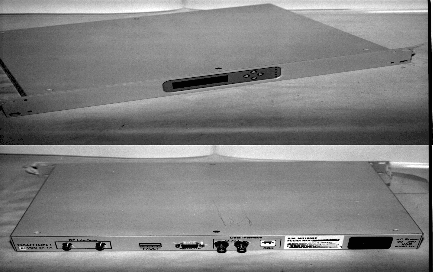
NK4-400011
May 19, 1999Wireless T1 Modem
Equipment Class
DSS - Part 15 Spread Spectrum Transmitter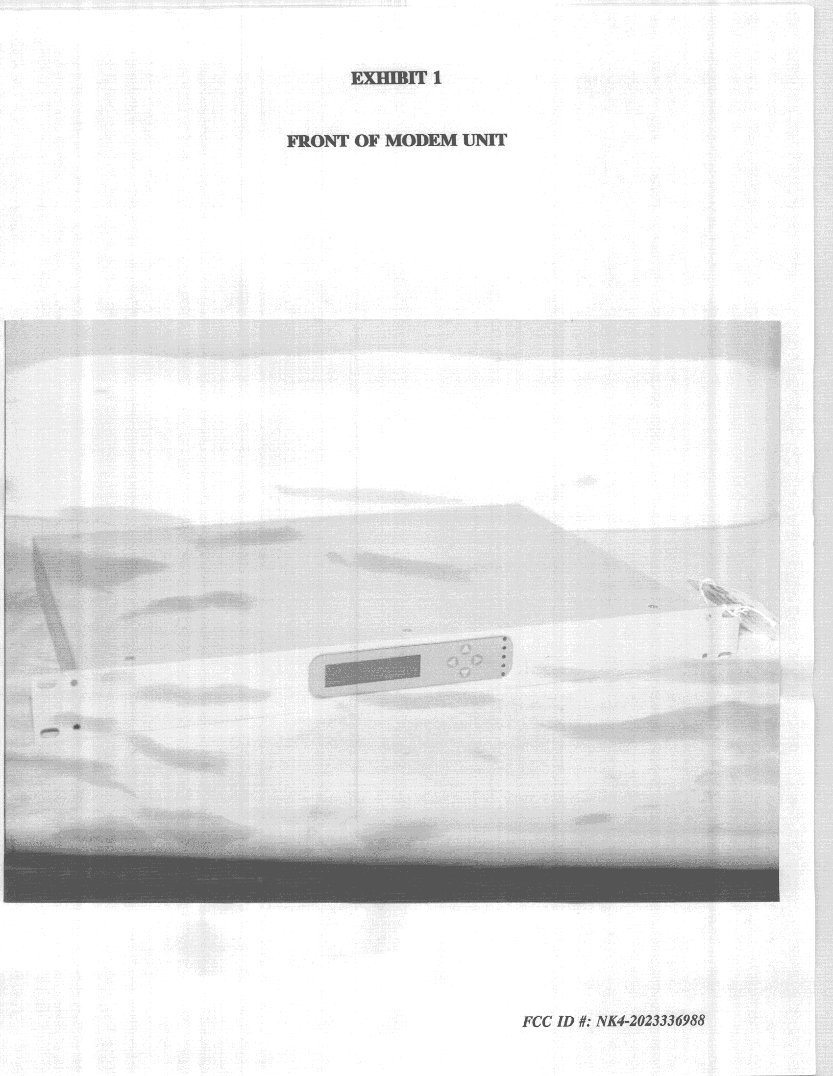
NK4-2023336988
Jan 14, 1999Data Transceiver
Equipment Class
DSS - Part 15 Spread Spectrum TransmitterNK4-202333WAVE
Sep 30, 1997Point-to-Point Communications Transmitter Maximum Output Power 50 mW This device must be professionally installed.
Equipment Class
DSS - Part 15 Spread Spectrum Transmitter