NMFAAGSM19500M2 Channel Amplifier/Antenna
Raytheon Company dba Raytheon Systems Co.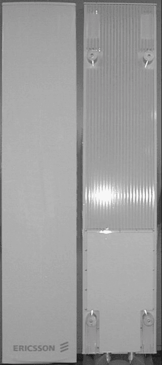
Click to zoom
Application Details
- Equipment Class
- PCB - PCS Licensed Transmitter
- Date of Grant
- Apr 04, 1999
- Application Purpose
- Original Equipment
- Date of Application
- Dec 15, 1998
- Equipment Note
- 2 Channel Amplifier/Antenna
- Frequency Range
- 1930.00000000 - 1990.00000000
- Country
- United States
Documents & Files
Document Text
Text extracted from the exhibit documents filed with the FCC. Open a document above to read the original.
Users Manual
Exhibit 8 Active Antenna Type Acceptance7/10/01 FCC ID NMFAAGSM191250M1 Exhibit 8External Photographs : 2.983 (g) Figure 8-1 Photographs of the Active Antenna Assembly RF Connections DC / Alarm Connection Locations for Type ID Labels
Block Diagram
Exhibit 2 Active Antenna FCC Type Acceptance7/10/01 FCC ID NMFAAGSM191250M 1 Exhibit 2Function of Each Active Circuit / Circuit Diagrams : 2.983 (d)-9, 7, 11 Exhibit 2 provides technical information on the function and design of each of the active circuits used in the Active Antenna. Specific items included in Exhibit 2 are listed following Included Items 1. HPA Circuit Card Assembly (CCA) 2. LNA Circuit Card Assembly (CCA) 3. DC / Fault Circuit Card Assembly (CCA) 4. Calibration Circuit Card Assembly (CCA) 5. Bandpass filter characteristics (2.983 (d) -11) 2-1 HPA Circuit Card Assembly (Power Amplifier, 2.4 Watt, Qty 3 per Channel) Figure 2-1 HPA CCA Block Diagram Three high power amplifier (HPA) cards are used in each transmit channel. Figure 2-1 shows a block diagram of the HPA circuit card assembly (CCA). Each HPA CCA is a three stage linear power amplifier with a rated power output of 35.5 ± 0.5 dBm. All three stages are Gallium Arsinide (GaAs) HFET type devices. The CCA includes on board power regulation, current sensing for fault isolation, an output isolator, and an adjustable attenuator used during manufacturing to adjust the power output to the nominal value noted. The input to the amplifier is through a 7db temperature compensating attenuator with a .007 dB/dB °C slope to flatten the response. The compensated amplifier produces the maximum output power at room temperature, where the output power is adjusted, and falls off at either temperature extreme. (See Figure 4-2 in Exhibit 4 for the amplifier’s temperature response.) The CCA uses 100% surface mount components. Circuit schematics are provided in Exhibit 3 and a photograph is included in Exhibit 9. Gain Adjust Attenuator Temperature Compensation DC Regulator + 7 VDC + 8 V (from DC/ Fault CCA) DC Regulator -5 VDC - 6V (from DC/ Fault CCA) RF In (from Tx Manifolds) RF Out (to antenna subarray panel) Current Sense (3 Pl) Fault Detection Circuitry Fault Out (to microprocessor on DC/Fault CCA) Gain Adjust Exhibit 2 Active Antenna FCC Type Acceptance7/10/01 FCC ID NMFAAGSM191250M 2 2-2 LNA Circuit Card Assembly (Low Noise Preamplifier, Qty 3 per Channel) Figure 2-2 LNA CCA Block Diagram Each of the two receive diversity channels utilizes three low noise amplifier (LNA) cards. Figure 2-2 shows a block diagram of the LNA circuit card assembly (CCA). The LNA CCA is a two stage low noise amplifier with a rated gain of approximately 26 dB. The CCA includes on board power regulation and current sensing for fault isolation. The CCA uses 100% surface mount components. Photographs and circuit schematics are shown in the “Internal Components” and “Schematics” exhibit files. Temperature Compensation DC Regulator +7 V + 9 V (from DC/ Fault CCA) RF In (from antenna subarray panel) RF Out (to Rx Combining Manifolds) Fault Detection Circuitry Current Sense (3 Pl) Fault Out (to microprocessor on DC/Fault CCA) Exhibit 2 Active Antenna FCC Type Acceptance7/10/01 FCC ID NMFAAGSM191250M 3 2-3 DC / Fault Circuit Card Assembly (Qty 1) The Active Antenna is powered by a DC/Fault circuit card. This card accepts the –48VDC prime power input supplied by the PBC and provides regulated, filtered drive voltages for the HPA and LNA circuit cards. Two redundant power supplies and filtering circuits are packaged on a single card to improve overall reliability of the system. If the primary supply fails, it is switched offline and the redundant supply takes over. Figure 2-3 shows a block diagram of the DC suppy portion of the circuit card. It contains switching DC - DC power converters running at 250 / 500 KHz, power regulation and filtering circuits, and surge suppression circuits. Figure 2-3 - DC/ Fault CCA Block Diagram OPT OPT OPTOPT UVLO FILTER +12 S S S S S S -6V LINEAR -8V LINEAR +5V LINEAR FLYBACK FLYBACK TXV+ CAL RXV - - +5 48 48 9V, 9V, 48 48 FUSE FUSE FUSE FUSE FUSE 48 48 48 9V, 9V, Exhibit 2 Active Antenna FCC Type Acceptance7/10/01 FCC ID NMFAAGSM191250M 4 The DC/Fault card also hosts the system control microprocessor. The microprocessor is a 16 bit Motorola 68HC12 running at 16 MHz. It handles the control commands from, and responses to the PBC via an RS-485 data link which runs over a single shielded twisted wire pair. During normal operation, the processor monitors discrete fault lines from the power supply and each of the amplifier circuits. It formats this information into two, 16 bit alarm response words that are supplied to the PBC upon interrogation, approximately once per second. On operator command, via the PBC control panel, the processor will also: supply the software version number, disable the HPA’s (in preparation for calibration), set the internal attenuators to the proper drive level, re-enable the HPA’s, set the internal attenuators to maximum (normal position when leaving the factory), and download an event log containing a limited history of commands, responses, and alarms. When commanded to set the attenuators, the controller begins the calibration sequence by automatically resetting the attenuators to their maximum value. It then steps the value down until a logic signal from the detector in the calibration circuit (see section 2-4) indicates that the drive level is correct to generate a 500 W EIRP signal from the HPA’s. The required attenuator setting for each channel is then written to non-voltile memory. If an acceptable level is not found, the attenuators are returned to the maximum value and a fault message is sent to the PBC. Circuit schematics are included in Exhibit 3 and a photograph of the card is shown in Exhibit 9. Exhibit 2 Active Antenna FCC Type Acceptance7/10/01 FCC ID NMFAAGSM191250M 5 2-4 Calibration Assembly (Qty 2, 1 per channel) Figure 2-4 shows a block diagram of the Calibration CCA. The calibration circuit for the Maxite system adjusts the input drive level so that the radiated power out of the amplifiers is 38.5 dBm ±0.3 dB at 25 C with any feeder cable loss between 0 and 12 dB between the Active Antenna…
Text truncated - open the document above for the full version.
Cover Letter(s)
WILEY, REIN & FIELDING 1776 K STREET, N.W. WASHINGTON, D.C. 20006 (202) 429-7000 THOMAS S. DOMBROWSKY , JR.FACSIMILE (202) 429-7236(202) 429-7049 TDOMBROW @WRF.COM Federal Communications Commission Equipment Approval Services P.O. Box 358313 Pittsburgh, PA 15251-5315 Re:Type Acceptance - Raytheon TI Systems, Inc. - Confidentiality Requested FCC ID: NMFAAGSM19500M Ladies and Gentlemen: Transmitted herewith on behalf of Raytheon TI Systems, Inc. ("RTIS"), is its application on FCC Form 731 requesting type acceptance of its Personal Communications Services (PCS) Active Antenna. A separate FCC Form 159 and check for $610 for the request for certification will be filed under separate cover. In accordance with Section 0.459 of the Commission's Rules, RTIS requests that certain specific technical information in the application be withheld from public inspection following grant of the application because the information contains confidential business information and/or trade secrets. These items, which are marked "CONFIDENTIAL" include: 1. Exhibit 3 - Active circuit schematics and assembly drawings that would disclose trade secrets associated with the manufacture of the device. 2. Exhibit 9 - Internal photographs of the unit. Significant effort and resources in research, development, and product design have been invested by RTIS and would be compromised if the materials for which confidentiality is requested were made available to competitors of RTIS as a result of this application. Accordingly, RTIS asks only that these specified items be held confidential after grant in order to maintain a fair and competitive marketplace. The $135 fee for confidentiality is included in the check referred to above. December 16, 1998 WILEY, REIN & FIELDING Error! No text of specified style in document. December 16, 1998 Page 2 If questions arise concerning this application, please contact Bruce Robidou of RTIS at 972-344-2348 or call me at 202-429-7236 (email: [email protected]). Respectfully, /s/ Thomas S. Dombrowsky, Jr. Engineering Advisor
External Photos
Exhibit 8 Active Antenna Type Acceptance7/10/01 FCC ID NMFAAGSM191250M1 Exhibit 8External Photographs : 2.983 (g) Figure 8-1 Photographs of the Active Antenna Assembly RF Connections DC / Alarm Connection Locations for Type ID Labels
ID Label/Location Info
Exhibit 1 Active Antenna Type Acceptance12/8/98 FCC ID NMFAAGSM191250M1 Exhibit 1ID Label & Location: 2.983 (f) Exhibit 1 includes drawings showing the format and placement of the ID labels. Included Items 1. Drawing of the Manufacturers Name Plate 2. Drawing of the Type ID Number Plate 3. Location of the Type ID Number Plate Items 1 and 2 are included in this Exhibit. The labels are located on the back of the AAU, near the bottom, as shown in assembly drawing 3233401, and in the excerpt below. The complete drawings are included in the drawing package provided with Exhibit 3. In addition to the Active Antenna Unit manufacturer’s labels listed above, the Maxite system provider will provide an AAU label including the following information: • Bar Code • Product number and revision status • Date of production • Product serial numbers • Corporate logo Figure 1-1 FCC ID Location , Base Module Caution Label UL Label Manufacturer’s Nameplate FCC ID Number Supplier’s Nameplate DW G NOSH 32333051 A P P L I C A T I O N NEXT ASSY USED ON REVDESCRIPTION DATEAPPROVED R E V I S I O N S © COPYRIGHT 1998 RAYTHEON ALL RIGHTS RESERVED. REV STATUS OF SHEETS REV SHEET ______ • DIMENSIONS ARE IN INCHES • PARENTHETICAL INFORMATION IS FOR REFERENCE ONLY • GENERAL TOLERANCES: DECIMALS .XX = ± .03, .XXX = ±.010, ANGLES ±1° UNLESS OTHERW ISE SPECIFIED CONTR DW N CHK ENGR PE&P APVD QA SCALESHEET DRAW ING NOCAGE CODE NONE 1 OF 6 A 3233305 96214 SIZE ______ DATE CM MCKINNEY, TEXAS CAD MAINTAINED. CHANGES SHALL BE INCORPORATED BY THE DESIGN ACTIVITY 32333003601C 32334003601C WORD FOR WINDOWS GENERATED110 A B C REVISION STATUS OF ALL SHEETS IS: - NONE T. DONALDSON98-10-28 LABEL, FCC ID DW G NO 3233305 SH 2 SCALE DW N ISSUE DATE DATE SHEET DW G NOCAGE CODE NONE 2 A 3233305 96214 REV - DALLAS, TEXAS SIZE TABLE OF CONTENTS 1.SCOPE ............................................................................................................................................ 3 2.APPLICABLE DOCUMENTS............................................................................................................ 3 2.1N ON -G OVERNMENT D OCUMENTS .................................................................................................. 3 3.REQUIREMENTS ............................................................................................................................ 3 3.1D IMENSIONS A ND C OLORS ............................................................................................................ 3 3.2M ARKING .................................................................................................................................... 3 3.3T OLERANCES .............................................................................................................................. 4 4.QUALITY ASSURANCE PROVISIONS ............................................................................................ 4 4.1I NSPECTION ................................................................................................................................4 4.2 F INAL A CCEPTANCE ..................................................................................................................... 4 5.PACKAGING.................................................................................................................................... 4 6.NOTES ............................................................................................................................................ 4 7. FIGURES ....................................................................................................................... 5 DW G NO 3233305 SH 3 SCALE DW N ISSUE DATE DATE SHEET DW G NOCAGE CODE NONE 3 A 3233305 96214 REV - DALLAS, TEXAS SIZE 1.SCOPE This specification establishes the requirements for decals for the Active Antenna Unit. 2.APPLICABLE DOCUMENTS 2.1Non-Government Documents The following documents form a part of the specification to the extent specified herein. In the event of any conflict between this document and the reference documents, this document shall govern. 3.REQUIREMENTS Materials shall be as specified herein. Materials and markings shall not blister, crack, or flow when exposed to temperatures from -40 deg C to +75 deg C. Materials shall be Flexcon 4 Mil White Vinyl with V23 acrylic permanent adhesive. 3.1Dimensions And Colors Dimensions and colors shall be in accordance with Figure 1 and 2. The color of the text in this drawing is black. 3.2Marking Decals shall be marked as shown in Figure 1 and 2. They shall be worded as shown with the number of lines as shown. All lettering on –1 and –2 shall be font point size 15 and bold. DW G NO 3233305 SH 4 SCALE DW N ISSUE DATE DATE SHEET DW G NOCAGE CODE NONE 4 A 3233305 96214 REV - DALLAS, TEXAS SIZE 3.3Tolerances Tolerances of dimensions shall be +/- .05 4.QUALITY ASSURANCE PROVISIONS 4.1Inspection Unless otherwise specified in the contract or purchase order. The manufacturer is responsible for the performance of all inspections necessary to ensure that the item meets the dimensional, material and finish, marking, and workmanship requirements for this specification. The supplier may use their own or any other facilities suitable for the performance of the inspection requirements. However, the procuring activity reserves the right to approve said facilities. The procuring activity reserves the right to perform any of the inspections set forth in this specification where such inspections are deemed necessary to assure supplies and services conform to prescribed requirements. 4.2 Final Acceptance Final acceptance shall be at the procuring activity. 5.PACKAGING Packaging shall be adequate to provide protection against any damage during shipment from the supply source to the ultimate using facility. Each package shall be marked with the manufacturer’s part number and the manufacturer’s identification. The markings shall be legible and permanent. 6.NOTES Identifica…
Text truncated - open the document above for the full version.
Operational Description
Active Antenna FCC Type Acceptance7/10/01 1 Raytheon TI Systems Smart Antenna Business Unit PCS 1900 Active antenna FCC Type Acceptance FCC ID NMFAAGSM19500M COPYRIGHT © 1998 RAYTHEON TI SYSTEMS ALL RIGHTS RESERVED Active Antenna FCC Type Acceptance7/10/01 FCC ID NMFAAGSM191250MPage 2 Of 19 Table of Contents Section I Introduction _________________________________________________________ 5 Section II Summary of Application _______________________________________________ 6 Section III Data ______________________________________________________________ 6 2.981Type Acceptance ___________________________________________________________ 6 2.983Application for Type Acceptance - Form 731 ___________________________________ 6 2.983 (a)Name of Applicant________________________________________________________ 7 2.983 (b)Identification of the Equipment _____________________________________________ 7 2.983 (c)Production is Planned _____________________________________________________ 7 2.983 (d)Technical Description _____________________________________________________ 8 2.983 (d) - 1Types of Emission___________________________________________________________ 11 2.983 (d) - 2Frequency Range____________________________________________________________ 11 2.983 (d) - 3Range of Operating Power ____________________________________________________ 11 2.983 (d) - 4Maximum Transmit Power Level ( 24.232 (d) 1640 W peak EIRP)_____________________ 11 2.983 (d) - 5DC Voltages and Current _____________________________________________________ 12 2.983 (d) - 6Function of Each Active Circuit ________________________________________________ 12 2.983 (d) - 7Circuit Diagrams ____________________________________________________________ 12 2.983 (d) - 8Users / Instruction Book ______________________________________________________ 13 2.983 (d) - 9Tune - up Procedure _________________________________________________________ 13 2.983 (d) - 10Frequency Stability _________________________________________________________ 13 2.983 (d) - 11Circuits for Suppression of Spurs, Limiting Modulation, or Power Limits_______________ 13 2.983 (d) - 12Digital Modulation _________________________________________________________ 13 2.983 (e)Data ________________________________________________________________________ 14 2.983 (f)ID Plate _____________________________________________________________________ 14 2.983 (g)Equipment Construction & Layout ________________________________________________ 14 2.983 (h)Encoder Device _______________________________________________________________ 14 2.983 (i)External RF Amplifier, Part 97 - Amateur Radio Service _______________________________ 14 2.983 (j)AM Broadcast - Stereo _________________________________________________________ 14 2.985 - 2.997Measurements Required ______________________________________________ 14 2.985 (a)Measurements Required: RF Power Output _________________________________________ 14 2.987Measurements Required : RF Modulation Characteristics ________________________________ 14 2.989Measurements Required: RF Occupied Bandwidth______________________________________ 15 2.991Measurements Required: Spurious Emissions at Antenna Terminals (24.238) ________________ 15 2.993Measurements Required: Field Strength of Spurious Radiation____________________________ 15 2.993 (a) Spurious Emissions Radiated Directly from the Cabinet _____________________________ 15 2.995Measurements Required: Frequency Stability __________________________________________ 16 2.997Frequency Spectrum to be Investigated_______________________________________________ 16 2.999Measurement Procedures _________________________________________________________ 16 2.948Description of Measurement Facilities ________________________________________ 17 24.51 (d)RF Radiation Hazard ____________________________________________________ 17 Section IV Exhibits __________________________________________________________ 18 Active Antenna FCC Type Acceptance7/10/01 FCC ID NMFAAGSM191250MPage 3 Of 19 Table of Figures FIGURE 1 ACTIVE ANTENNA AND RELATED EQUIPMENT5 FIGURE 2 ACTIVE ANTENNA FUNCTIONAL BLOCK DIAGRAM8 FIGURE 3 SIGNAL FLOW DIAGRAM9 FIGURE 4 OPERATING FREQUENCY BANDS11 Active Antenna FCC Type Acceptance7/10/01 FCC ID NMFAAGSM191250MPage 4 Of 19 Table of Exhibits The following list of exhibit files have been submitted as supplements to this report: EXHIBIT 1 ID LABEL & LOCATION: 2.983 (f) EXHIBIT 2 BLOCK DIAGRAMS: 2.983 (d)-9,11 EXHIBIT 3 SCHEMATICS: 2.983 (d)-7 EXHIBIT 4 RF POWER OUTPUT: 2.983 (d)-3,4, 2.985 (a) EXHIBIT 5 SPURIOUS EMISSIONS: 2.991 (a), 2.993 (a) EXHIBIT 6 KTL REPORT- EMISSIONS :2.993 EXHIBIT 7 OPERATIONAL INSTRUCTIONS: 2.983 (d)-8 EXHIBIT 8 EXTERNAL PHOTOS: 2.983 (g) EXHIBIT 9 INTERNAL PHOTOGRAPHS: 2.983 (g) Active Antenna FCC Type Acceptance7/10/01 FCC ID NMFAAGSM191250MPage 5 Of 19 Section IIntroduction This Type Acceptance application describes an Active Antenna with 500 Watts EIRP output and integrated low noise preamplification on receive for use in mobile wireless communications infrastructure. It operates in the 1900 MHz spectrum allocated to Broadband PCS (Personal Communication Systems). The Active Antenna applies Active Phased Array Antenna technology to the problem of improving the coverage and useful communications range of fixed infrastructure radio equipment. It is designed to work as an option with the Ericsson 2302 Radio Base Station (RBS) and Power Battery Cabinet (PBC). The Radio Base Station provides the signals for amplification while the Power Battery Cabinet provides the DC power and alarming interface for the Active Antenna. Figure 1 illustrates the Active Antenna and the related equipment. This product is similar to a previous Raytheon TI Systems (RTIS) Active Antenna product (reference FCC ID NMFAAGS1912501C1B) but it receives its power and control signals directly from the Ericsson PBC, whereas the previous product provided these functions with an additional, external interf…
Text truncated - open the document above for the full version.
Parts List/Tune Up Info
Exhibit 4 Active Antenna FCC Type Acceptance7/10/01 FCC ID NMFAAGSM191250M 1 Exhibit 4RF Power Output: 2.983 (d)-3, 2.983 (d) -4, 2.985 (a) The Active Antenna complies with the maximum EIRP limit of 1640 Watts as specified in 47 CFR 24.232. The EIRP of the Active Antenna is determined by the sum of combined output power of the internal transmit amplifiers and the gain of the radiating array. This exhibit provides measurements of: the combined output power of the amplifiers as measured in the laboratory, the gain of the radiating array, and field measurements of the total, combined EIRP Each set of data includes a block diagram of the test set up, list of test equipment, description of the test sequence, and test data. Specific items included in Exhibit 4 are listed following. Included Items 1. RF power Output at the Combined Amplifier Power Reference Point - 2.983(d)-3 2. Range measurement of radiating elements 3. Active Antenna RF power output - field measurements Exhibit 4 Active Antenna FCC Type Acceptance7/10/01 FCC ID NMFAAGSM191250M 2 4-1 RF Power Output at the Combined Amplifier Power Reference Point - 2.983(d)-3 The Active Antenna contains three amplifier channels, each of which is connected to an antenna subarray of four radiating elements. To measure the combined RF output power, the antenna elements are removed and a passive test combiner of known loss is used to sum the output of the three amplifiers into a single output. The unit was measured in a temperature chamber and RF output data was collected at three temperatures, -35 ° C, +25 °C, and + 55 ° C. For each test, the input port of the Active Antenna is driven with an unmodulated signal source at +20.5 dBm (100 mW) power input which allows the sum of the power amplifiers to reach full rated power of 38.5 dBm (7.1 W) total. The test diagram is shown in Figure 4-1 and the list of test equipment is provided at the end of this exhibit. Figure 4-1 Test Configuration for RF Power Output Sum Path Measurements HP - 8508A / 85082A Vector Voltmeter / 2 GHz Module Controller HPVEE Software HPIB Bus Card HP - 8657B Signal Generator 30 db Coupler PA Load Circ Tx Input Temperature Chamber Path 4 Out Path 3 Out Path 2 Out Active Antenna Electronics HPIB Bus 30 db Coupler Atten Load HP - E3601A DC Pwr Supply +48V DC HP - 437B Power Meter Calibration Path Sum Test Combiner Exhibit 4 Active Antenna FCC Type Acceptance7/10/01 FCC ID NMFAAGSM191250M 3 Test Data; Measured RF power out is shown in Figures 4-2, 3 and Tables 4-1, 2. The data shows the power to be within acceptable tolerances over the frequency band and operational temperature range. Figure 4-2 RF Power Output over Temperature – Channel 1 Frequency (MHz) Temperature CPower Output (dBm) 1950 -35 ° C 38.4 1950 +25 ° C 39.0 1950 +55 ° C 38.4 1960 -35 ° C 38.1 1960 +25 ° C 38.9 1960 +55 ° C 38.3 1970 -35 ° C 38.3 1970 +25 ° C 38.8 1970 +55 ° C 38.2 Table 4-1 RF Power Output Combined Power Output over Temperature Transmit Channel 1 36.0 36.5 37.0 37.5 38.0 38.5 39.0 39.5 40.0 19501955196019651970 Frequency Power Out (dBm) 55 C 25 C -34 C Exhibit 4 Active Antenna FCC Type Acceptance7/10/01 FCC ID NMFAAGSM191250M 4 Figure 4-3 RF Power Output over Temperature – Channel 2 Frequency (MHz) Temperature CPower Output (dBm) 1950 -35 ° C 37.5 1950 +25 ° C 38.3 1950 +55 ° C 37.7 1960 -35 ° C 37.3 1960 +25 ° C 38.2 1960 +55 ° C 37.6 1970 -35 ° C 37.0 1970 +25 ° C 37.8 1970 +55 ° C 37.3 Table 4-2 RF Power Output Combined Power Output over Temperature Transmit Channel 2 36.0 36.5 37.0 37.5 38.0 38.5 39.0 39.5 40.0 19501955196019651970 Frequency Power Out (dBm) 55 C 25 C -34 C Exhibit 4 Active Antenna FCC Type Acceptance7/10/01 FCC ID NMFAAGSM191250M 5 4-2 Range measurement of the radiating elements The radiating elements for the Active Antenna are aperture coupled patch arrays with a nominal 3 dB horizontal beamwidth of 65 degrees and a peak gain of 18.5 dBi. Figure 4-3 shows the measured field pattern of the aperture. Figures 4-4 shows a far field measurement of the isotropic gain of the transmit aperture. The gain of the transmit array is within the production limits discussed in section 2-983(d)-4 of this report, i.e. 18.5 +/- 0.5 dB. 10 20 30 40 50 30 210 60 240 90 270 120 300 150 330 180 0 Figure 4-3- Measured Horizontal Radiation Pattern of the Active Antenna Aperture Figure 4-4 Measured Gain of the Transmit Antenna 4-3 Active Antenna EIRP measurements Gain of the Transmit Apertures 16.00 16.50 17.00 17.50 18.00 18.50 19.00 19.50 20.00 1.9301.9401.9501.9601.9701.9801.990 Frequency (GHz) Gain (dBi) Trans m it Ch 1 Trans m it Ch 2 Exhibit 4 Active Antenna FCC Type Acceptance7/10/01 FCC ID NMFAAGSM191250M 6 The sum of the RF output power (+38.5 dBm) and the isotropic antenna gain (18.5 dBi), provides the total EIRP of 57 dBm. To confirm this measurement, the EIRP of the complete system was measured on a far field antenna range. To measure EIRP, the antennas are mounted on a 100’ antenna test tower with the receiving equipment located on a similar tower, 400’ downrange. Reflection fences are used to minimize ground reflections. First, a signal source is configured to deliver a fixed power between 20.5 and 32.5 dBm into a reference antenna with a known gain. The received signal strength is then measured downrange at 5 MHz increments across the appropriate sub-band. The reference antenna is then replaced with the Active Antenna. The Active Antenna is commanded to calibrate the input drive level and the internal attenuator settings are noted. The new received signal strength is then recorded at each frequency. From this, the EIRP of the Active Antenna is calculated by adding the difference in received power levels and the internal attenuator settings to the gain of the reference antenna. The test unit was configured with a set of filters for each of the three bands. Results for these measurements are given in Figures 4-5, 4-6, and 4-7. All three bands are in compliance with the +62 dB (1640 W) limit…
Text truncated - open the document above for the full version.
Test Report
Exhibit 5 Active Antenna FCC Type Acceptance7/10/01 FCC ID NMFAAGSM191250M 8 Exhibit 5Spurious Emissions,- 2.991, 2.993 (a), 2.997 Exhibit 5 provides measurements of spurious emissions both in the laboratory and in the field. Each set of data includes a block diagram of the test set up, list of test equipment, description of the test sequence, and test data. Specific items included in Exhibit 5 are listed following. Included Items 1. Spurious Emissions at the Antenna terminals 2. Spurious Emissions Radiated Directly from the Cabinet 3. Spurious Emissions - Field Measurements Exhibit 5 Active Antenna FCC Type Acceptance7/10/01 FCC ID NMFAAGSM191250M 9 5-1 Spurious Emissions at the Antenna Terminals Test Configurations The Active Antenna has two transmit paths, each of which contains three amplifiers. Each amplifier is connected to a subarray of four antenna elements. To measure the purity of the output spectrum of the power amplifiers, it is necessary to disconnect the antenna and observe the spectrum of each of the three channels at the filter output coaxial connection where the normal attachment to the radiating elements is made. The amplifiers were driven to their maximum rated output power (2.4 Watts each) with a GMSK modulated signal source and the output spectrum was measured from 10 Khz to 20 Ghz. Data was collected at each of the five output ports for both transmit paths. Figure 5-1 shows the test configuration. Lists of test equipment and calibration data are included at the end of this section. Figure 5-1 Test Configuration for Spurious Emissions at the Antenna Terminals Test Results The limit on spurious emissions was computed from 47 CFR 24.238 to be 43 + 10 log P, where P is the combined output power of the five amplifiers (7.1 W), or 43 + 10 log (7.1) = -51.5 dBc. The spectrum was observed to a level of -70 dBc. Test results showed no observable spurious energy at the antenna terminals for any of the five channels on either transmit path. Based on this the Active Antenna’s amplifiers were determined to be compliant with the limitations on spurious energy. HP - 8657B Signal Generator PA Load HP - 8508 A / 85082A Vector Voltmeter / 2 GHz Module Controller HPVEE Data Collection SW GPIB Bus Card Circ Tx Input Path 3 Out Path 2 Out Path 1 Out Active Antenna HPIB Bus Test Path 1 of 5 HP - 8564E 40 GHz Spectrum Analyzer HPIB Bus Atten 33 dB BandPass Filter Test Path 2 of 5 Test Path 3 of 5 30 db Coupler Exhibit 5 Active Antenna FCC Type Acceptance7/10/01 FCC ID NMFAAGSM191250M 10 An example plot showing the results for one amplifier is shown in Figure 5-2. The vertical scale shows the signal level with respect to the carrier (dBc) from +5 to –80 dBc in 10 dB divisions. The horizontal scale shows frequency in GHz from 0 to 20 GHz, with the carrier visible just below 2 GHz. Resolution bandwidth and video bandwidth are noted at the bottom of the chart, with both set at 1 MHz. The only energy visible is the noise floor of the spectrum analyzer at approximately –63 dBc, showing the amplifier to be well within the specified limitations. Figure 5-2 Band 2 Power Amplifier Output Spectra 10 KHz - 20 GHz with Modulated Signal Input Figure 5-3 shows the same measurement with the resolution bandwidth decreased to 300 kHz (approximately the bandwidth of the input signal) to lower the noise floor. No reportable spurs were observed. Figure 5-3 Band 2 Power Amplifier Output Spectra 10 kHz – 20 GHz with Modulated Signal Input Pl…
Text truncated - open the document above for the full version.
Contact Information
Applicant
Earl D. Munns(Counsel)
Technical Contact
Raytheon TI Systems, Inc.Paul Golemon
[email protected]972-344-2364
17217 Waterview Parkway, MS 333 · Dallas, Texas · United States
Non-Technical Contact
Raytheon TI Systems, Inc.Bruce Robidou
[email protected]972-344-2348
Test Firm
Nemko Dallas, Inc.Michael Cantwell
Technical Specifications
| # | Rule Parts | Frequency Range | Power Output | Emission | Tolerance |
|---|---|---|---|---|---|
| 1 | 24E | 1.93 GHz - 1.99 GHz | 7.1 W | GXW | Amp |
Other Applications from Raytheon Company dba Raytheon Systems Co.

NMF-CT2-001
Jan 18, 1999Cellular Transceiver with Modem
Equipment Class
TNB - Licensed Non-Broadcast Station TransmitterNMFAAGS1912501C1B
Feb 02, 1998Single Channel Amplifier/Antenna Approved for use with PCS-1900 emissions (GXW).
Equipment Class
PCB - PCS Licensed Transmitter