NTRNSA2010
Niigata Seimitsu Co Ltd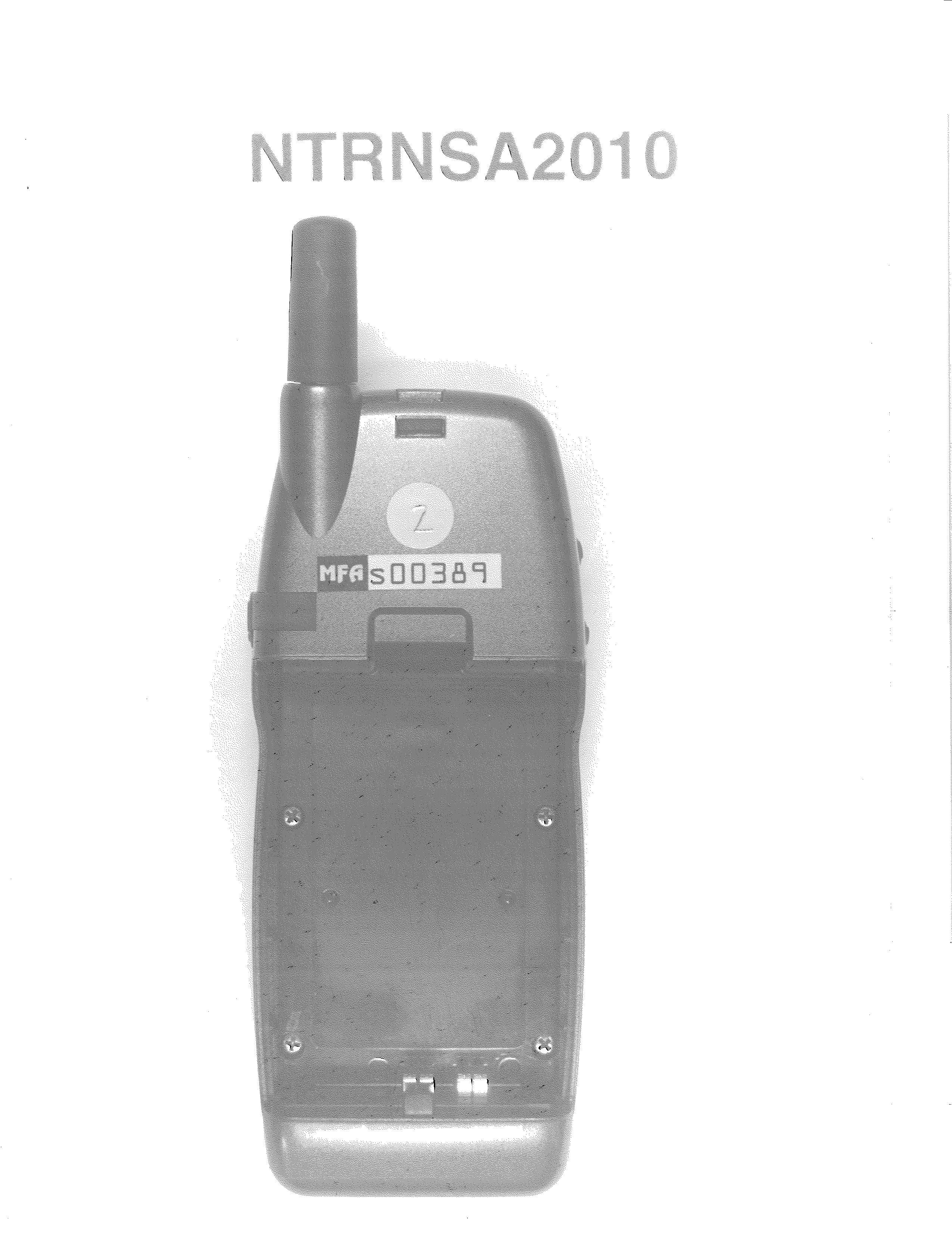
Click to zoom
Application Details
- Equipment Class
- TNE - Licensed Non-Broadcast Transmitter Held to Ear
- Date of Grant
- Nov 14, 1999
- Application Purpose
- Original Equipment
- Date of Application
- Sep 26, 1999
- Frequency Range
- 824.04000000 - 848.97000000
- Company
- Niigata Seimitsu Co Ltd
- Country
- Japan
Documents & Files
Document Text
Text extracted from the exhibit documents filed with the FCC. Open a document above to read the original.
ID Label/Location Info
COMPLIANCE STATEMENT: This device complies with Part 15 of the FCC Rules. Operation is subject to the condition that this device does not cause harmful interference. THIS DEVICE COMPLIES WITH PART 15 OF FCC RULES AND WITH RSS- 210 OF INDUSTRY AND SCIENCE CANADA. OPERATION IS SUBJECT TO THE FOLLOWING TWO CONDITIONS: (1) THIS DEVICE MAY NOT CAUSE INTERFERENCE, AND (2) THIS DEVICE MUST ACCEPT ANY INTERFERENCE, INCLUDING INTERFERENCE THAT MAY CAUSE UNDESIRED OPERATION OF THIS DEVICE. ISC: RSS/CNR 210
ID Label/Location Info
FCC ID: NTRNSA2010 COMPLIANCE STATEMENT LABEL POSITION REQUEST Gentlemen: In regards to the compliance statement label placement, Niigata Seimitsu requests placing the compliance label onto the manual due to extreme size limitations of the NSA2010 portable cellular telephone. Best regards, Royce Fowler
Operational Description
NSA2010 System Description (refer to the block diagram) 1.1 Receiver (RX) section 1.1.1 Input ( receiving frequency) fri=869.040 to 893.970 MHz, 30KHz step 1.1.2 Description The RX signal caught by Helical antenna is fed to RX RF amplifier and mixer (Q101,Q121) through the duplexer (F100) with band-pass filtering. ‡ See characteristics of the duplexer (DFYGR836CR881NHA). Then the RX signal amplified by Q101 and applied to RX mixer1, Q121 (RX MIX1) through the SAW band-pass filter (F102) which reduces out of band noises and spurious. ‡ See characteristics of the SAW band-pass filter. The signal of input is mixed with the local frequency (fo1) which is generated by the VCO (X911) that works as a frequency synthesizer combined with phase locked loop IC, U900, at the first mixer Q121. The output of the first mixer generates first IF frequency (fi1) , 86.460MHz and this signal is delivered to the first IF filter (F102). The fi1 and fo1 is calculated as below; The second IF frequency fi2=60KHz The second local frequency fo2= 14.4MHz(TCXO frequency) x6 =86.400MHz Therefore, fi1= fi2 + fo2 =86.460 MHz Therefore, fo2=fri + fi1 =955.500 to 980.430MHz, 30KHz step The F102 is a SAW filter with 86.460MHz of center frequency that has very good shape factor. This filter works to eliminate alternate frequency (fi1+/- 60KHz) and image frequency of second mixer (fi1+120KHz=86.58MHz) that rejection ratio should satisfy the specification. ‡ See characteristics of the SAW IF filter. The fi1 signal is amplified by Q131 in order to obtain enough gain of RX section. The IC, U101, is incorporating the following function; Second Mixer with image frequency cancellation circuit, Band-pass filter with 60KHz of center frequency Second IF amplifier FM detector RSSI (Receiving Signal Strength Indicator) output) ‡ See block diagram and characteristics of TA31181FN. The second local frequency (fo2=86.460MHz) is obtained to be multiplied by six(6) of TCXO frequency (f TCXO=14.4000MHz). The f TCXO is fed to tuned amplifier inside of U900 and Q171. The about 86 MHz tuning circuit, L171, L172, C174 and C175, picks up the 86.400MHz which is a six times harmonics of f TCXO. The second mixer inside of U101 generates a second IF signal which frequency is 60KHz The fo2 is split into 2 path inside of U101, one for in-phase signal and other for quadrature signal. These signals are applied to two second mixers. The output of second mixers is synthesized with 90 degrees phase shifting for quadrature mixer side. This function works to make cancellation of the image frequency, about 30dB rejection ratio. About 75 dB total image rejection ratio for fi2 can be obtained to combine with F102, even though such lower IF frequency. The sharp narrow (+/-15KHz) BPF having 60KHz-center frequency inside U101 works to eliminate adjacent channel. The center frequency of 60KHz BPF is synchronizing to its clock frequency, 14.400MHz that is fed from TCXO. So very stable filter characteristics can be obtained due to very stable frequency of TCXO. After 60KHz filtering, the signal is amplified and limiting its amplitude by limiter. Then quadrature detector that is incorporated into U101 demodulates the FM signal. The center frequency is also synchronizing to 14.4 MHz like 60KHz filter. RSSI (DC level) is obtained to gather second IF signal. 1.2 Transmitting (TX) section 1.2.1 TX frequency ftx= 824.040 to 848.940MHz, 30KHz step 1.2.2 Activation control for the transmitter When TX starts to activate, TX VCO and TX section of the U101 simultaneously. The TX VCO is switched by Q701 that is controlled by CPU with active high level, and TX section synthesizer of U101 can be controlled by data from CPU through its serial data transmission line, SYE, SYD and SYC. After a few milliseconds waiting, the TX switch, Q606 and Q607 work to turn on. Then all TX sections as U201 (buffer amplifier), Q603 (TX driver), Q604 ( TX final power amplifier), U241 (APC circuit) Q607 and Q606 (power switch) become to activate. Note that TX switch circuit, Q606 and Q607 are not switched on if TX synthesizer circuit including VCO has already activating. The synthesizer must be priority in order to activate all TX circuits. The emitter of Q607 detects whether synthesizer is activating, i.e., Q607 must be low level for activation. Usually it is switched on; then, enough current capacity is applied to final stage of TX power amplifier VCC (6.0V). 1.2.3 TX VCO and Modulator The basic TX VCO circuit is built of X931. It is controlled by applied DC voltage that is the output of the synthesizer, U900, through low pass filter, C939, C935, R932, R933 and C933. The controlled voltage is within 0.8 to 2.2V to cover the TX frequency range. The CPU is monitoring synthesizer lock-upped DC voltage through the TVL line. If this voltage is out of 0.8 to 1.0 volt at minimum frequency, CH0991, the DC voltage to TX V.C.O applied from CPU through TVA line is adjusted until becoming specified range since this loop works as negative feedback circuitry. After fixing DC voltage at CH0991, the synthesizer frequency moves to upper frequency, CH0799 and monitored this frequency by CPU through TLV line. If this DC voltage is lower than 2.2volt, this VCO is accepted, otherwise, higher than 2.2V, this is failure VCO and rejected. At the same time, lock condition is monitored by CPU and unconditionally is rejected if unlocked condition occurs. TX V.C.O is also used for the modulator. The modulation signal comes from the base band processor through MOD line. R401 and R934 to be obtained optimized modulation level divide this signal. ‡ Refer to paragraph of Modulation 1.2.4 TX power stage The fig.1.2.4.1 shows block diagram of TX power stage for NSA2010. The modulated FM signal generated by TX VCO is amplified by U201 and obtained about 10mW (10dBm) output power on U201. And about 5mW (7 dBm) that drives driver transistor, Q603, is obtained at the output F201 which has about -3 dB gain. SMOOTHER VCO MOD MATCH NET. M…
Text truncated - open the document above for the full version.
Parts List/Tune Up Info
POWER OUTPUT 2.985 FCC PART 22,SUBPART H 50 OHM LOAD RF COMMUNICATIONS TEST SET ATTENUATOR RF POWER METER ANT. OUT E.U.T. INTERFACE CONNECTOR VARIABLE POWER SUPPLY BATTERY PACK PROJECT No.NSA2010 FCC ID:NRTNSA2010 (Vcc 3.8V) (3.8V) PAGE No.37 50 OHM LOAD AUDIO FREQUENCY RESPONSE 2.987(a) MODULATION LIMITING 2.897(b) ANT. OUT MODULATION METER ATTENUATOR RF COMMUNICATIONS TEST SET AUDIO GENERATOR VARIABLE POWER SUPPLY FCC PART 22,SUBPART H E.U.T. Interface Connector BATTERY PACK PROJECT NO,NSA2010 FCC ID:NRTNSA2010 External Audio input Vcc 3.8V PAGE No.38 3.8V E.U.T. Interfase Connector AC VOLTAGE MATER AUDIO GENERATOR RF COMMUNICATIONS TEST SET VARIABLE POWER SUPPLY BATTERY PACK PROJECT NO,NSA2010 FCC ID:NTRNSA2010 Extermal Audio input Vcc 3.8V Moduiation signal moniter output PAGE No.39 3.8V OCCUPIED BANDWIDTH 2.989(c)(1) SPURIOS EMSSIONS 2.991 6dB ATTENUATOR SPECTRUM ANALYZER OR TEST RECEIVER ANT. OUT E.U.T. AUDIO GENERATOR Interfase Connector RF COMMUNICATIONS TSET SET VAARIABLE POWER SUPPLY BATTERY PACK PROJECT No.NSA2010 FCC ID:NTRNSA2010 External Audio Input Vcc 3.8V PAGE No.40 3.8V PAGE No.42 CLIMATE CRAMBER RF COMMUNICATIONS TEST SET ATTENUATOR FREQUENCY COUNTER E.U.I. ANT. OUT VARIABLE POWER SUPPLY FCC PART 22,SUBPART H BATTERY PACK PROJECT No.NSA2010 FCC ID:NRTNSA2010 Vcc 3.8V 3.8V PAGE No.41 How to use test command for NSA2010 This paper describes test command operation for the AMPS cellular phone, NSA2010. 1. To enter test mode 1.1 The unit must be standing at idling mode before entering test mode. 1.2 Press the key pads as following sequence when entering test mode. [5][4][#][3][MENU][2][#]; [ ] means key pad 1.3 You can see a message , shown in below, on the LCD after completed above key entry. " TEST MODE " Now, you are in test mode and can start test the unit using test command in accordance with TEST COMMAND LIST on attacked. 2. To set command for making test conditions The test command set can be achieved as following key operations; [c][d][SEND][nn] where;c = first digit of the Command d = second digit of the Command SEND = key of STR nn = added any bits sub data (if required) The codes are assigned to key pads as following; Code assigned key Codeassigned key 0 - 9 0 - 9 D MAIL A * E MEM B # F MENU C CLR PAGE No.43 Mode: M0 ; Send command without sub code (nn) M1 ; Send command with sub code (nn) M2 ; Send command and display data status on the LCD note: the data on test command list, "1d" means 0.5 byte (= 1 digit) for key entry and 1 byte for data input by UART. 3. Example You want to obtain; transmitting with , channel = 383, RF attenuation (power level )= 0, modulation = Signaling Tone , ST The setting sequence is; * Load synthesizer with channel 383 * Set attenuation * Set ST * Carrier on The key sequence is; [8][3][SEND][0][3][8][3][8][4][SEND][0][8][F][SEND][8][1][SEND] Note that set commands remain until release command added PAGE No.44 PAGE No.45 Interface Connector STATUS (5F,0,3) FORMATSTATUS (5F,0,3) FORMAT Bit76543210 Byte1S7S6S5S4S3S2S1S0 Byte2C1C20CARRTN0S9S8 Byte3PL2PL1PL0BIMODEWSRXMTXM S9..S0S9..S0Channel Number bits(Binary coded representation of Channel number S9 = MSB Pl2,1,0Pl2,1,0Power level bits(PL0 - 7, PL2=MSB, Carrier=1(ON)) CARRCARRCarrier(1=ON) TNTNSignaling Tone (ST: 1=ON) TXMTXMTX Audio Mute (1=muted) TXMTXMRX Audio Mute (1=muted) WSWSWord Synchronization (1=WS acquired) MODEMODE1=Control Channel, 0=Voice channel) BIBICurrent state of the majority voted B/I bit (0=Busy, 1=Idle) C1,C2C1,C2SAT Frequency is encoded as follows; C1C2Frequency 005970Hz 016000Hz 106030Hz 11No SAT Lock DTMF FREQUENCYDTMF FREQUENCY Lable ofAssigned Frequencies KeyHT(Hz)LT(Hz) 11209697 21336697 31447697 41209770 51336770 61477770 71209852 81336852 91477852 *1209941 01336941 #1477941 Connection pin # Function 1VD(Digital voltage) 2SWEV(External voltage switch) 3RST(System reset) 4VSNS(Voltage sense) 5VP(Programming voltage 6VCC (3.8V Power Supply) 7RMUTO ( Radio mute control output) 8RSSIV( RSSI DC voltage output) 9AFI(Audio input) 10Mode (Modulation signal monitor output) 11IGNS( Ignition sense input for Hands free operation) 12AFO (Audio output) 13RXD (UART reception) 14TXD (UART transmission) 15HFS (Hands Free sense) 16GND (Ground) I/F ConnectorI/F Connector Cable to TU
Parts List/Tune Up Info
NSA2010 ADJUSTMENT AND MEASUREMENT GUIDE <Key operation> <Function/LCD indication> 1: [Power Switch]..............................No Service 2: ~KeyRubberSwitch~ [5]+[4]+[#]+[3]+[MENU]+[2]+[#]......Test Mode 3: [MENU]+[MEM]+[SEND] ...............Align Mode 4: [CLR] ........................................01-255 5: [CLR] ........................................02-255 6: [CLR] ........................................03-TCXO-F Then, transmit output power (CH0799), 848.970000MHZ is generated. In case of generating a frequency shift, adjust the frequency according to the following method. ADJUSTMENT PROCEDURES: Generating high shift, → push [<∗] key (the frequency goes down) Generating low shift, → push [#>] key (the frequency goes up) →To fix the adjustment, push [MENU] key. 7: [CLR]........................................04-DEMOD Adjust SG Input to 50dBm CH0384 (881.52MHZ). Deviation-2.9kHZ DeviationFrequency-1kHZ Adjust AF output to 110mA±5mA 8: [CLR]........................................05-PL0-LOW Adjust output to 620mW±10mW c.f How to adjust 9: [CLR] ........................................06-PL3-LOW Adjust output to 250mW±10mW c.f How to adjust 10: [CLR] ........................................07-PL4-LOW Adjust output to 100mW±10mW c.f How to adjust 11: [CLR] ........................................08-PL5-LOW Adjust output to 40mW±0.5mW c.f How to adjust 12: [CLR] ........................................09-PL6-LOW Adjust output 16mW±0.8mW c.f How to adjust 13: [CLR] ........................................10-PL7-LOW Adjust output 6.0mW±0.6mW c.f How to adjust 14: [CLR]........................................11-PL0-MID Adjust output to 620mW±10mW c.f How to adjust 15 [CLR] ........................................12-PL3-MID Adjust output to 250mW±10mW c.f How to adjust 16: [CLR] ........................................13-PL4-MID Adjust output to 100mW±10mW c.f How to adjust 17: [CLR] ........................................14-PL5-MID Adjust output to 40mW±0.5mW c.f How to adjust 18: [CLR] ........................................15-PL6-MID Adjust output 16mW±0.8mW c.f How to adjust 19: [CLR] ........................................16-PL7-MID Adjust output 6.0mW±0.6mW c.f How to adjust 20: [CLR].........................................17-PL0-HI Adjust output to 620mW±10mW c.f How to adjust 21: [CLR].........................................18-PL3-HI Adjust output to 250mW±10mW c.f How to adjust 22: [CLR] .........................................19-PL4-HI Adjust output to 100mW±10mW c.f How to adjust 23: [CLR] .........................................20-PL5-HI Adjust output to 40mW±0.5mW c.f How to adjust 24: [CLR] .........................................21-PL6-HI Adjust output 16mW±0.8mW c.f How to adjust 25: [CLR] .........................................22-PL7-HI Adjust output 6.0mW±0.6mW c.f How to adjust 26: [CLR] ........................................23-LIMIT-L 27: [CLR].........................................24-LIMIT-M 28: [CLR].........................................25-LIMIT-H LIMIT has three channels LIMIT- Low, Middle, High. Adjust Max Deviation in this channel to 10.8khz±0.5khz. <Test Condition> ~H/P 8920B~ Input level: 121dBmV IF Filter: 230KHz Filter1: 50HZ HPF Filter2: 15KHZ LPF De-Emphasis: OFF 29: [CLR] ........................................26-ST-LOW 30: [CLR].........................................27-ST-MID 31: [CLR].........................................28-ST-HI ST has three channels ST-Low, Middle, High. In this channel (low), adjust signal tone deviation. Adjust Max Deviation 8.0±0.2Khz. <Test Condition> ~H/P 8920B~ External Input: OFF IF Filter: 230KHz Filter1: 300HZ HPF Filter2: 15KH LPF De-Emphasis: OFF 32: [CLR] ........................................29-SAT-LOW 33: [CLR].........................................30-SAT-MID 34: [CLR].........................................31-SAT-HI SAT has three channels SAT-Low, Middle, High. In this channel, adjust SAT Deviation to 2.0kHz/2.3kHz <Test Condition> ~H/P 8920B~ External Input: OFF IF Filter: 15 kHz Filter1: less than 20 HZ HPF/300Hz HPF Filter2: 6KBPF/15kHz LPF De-Emphasis: OFF 35: [CLR]...........................................32-VOICE-L 36: [CLR]...........................................33-VOICE-M 37: [CLR]...........................................34-VOICE-H Voice has three channels VOICE-Low, Middle, High. In this channel, adjust VOI-EXT Deviation to 2.9kHz. <Test Condition> ~H/P 8920B~ Input level: 99dBuV IF Filter: 15kHz Filter1: C MESSAGE Filter2: 99K LPF De-Emphasis: OFF 38: [CLR]............................................35-DTMF-LO 39: [CLR]............................................36-DTMF-MI 40: [CLR]............................................37-DTMF-HI DTMF has three channels, Low, Middle, High. In this channel, adjust Deviation to 8.6kHz. <Test Condition> ~H/P 8920B~ External Input: OFF IF Filter: 230kHz Filter1: 300HPF Filter2: 3K LPF De-Emphasis: OFF 41: [CLR]............................................40-ANT-2 Antenna display 2: –110dBm 42: [CLR]............................................41-ANT-3 Antenna display 3: -100dBm 43: [CLR]............................................42-ANT-4 Antenna display 4: -90dBm That is all to adjust for NSA2010. The other channels have nothing to do with this function set, so please do not touch them.
Parts List/Tune Up Info
ACTIVE DEVICE 1/2 Ref. No.Part TypeDescription B551PAS614-VL3BATTERY D2411SS345 DIODE D401DA221 DIODE D402DA221 DIODE D403DAP222 DIODE D404DAP222 DIODE D405UMN1N DIODE D406RB715F DIODE F100TDPF-836E-12 DUPLEXER, AMPS F102EFCH86MMQW2 IF SAW FILTER F201SAFC836.5MA90N RF SAW FILTER F202PTHM1616C-FR80A Coupler F203SAFC881.5MC90T RF SAW FILTER L101LC8N2 INDUCTOR L401LQG21C470N00 INDUCTOR Q1012SC5185 TRANSISTOR Q1022SC5186 TRANSISTOR Q1032SC4725 TRANSISTOR Q1042SC4725 TRANSISTOR Q1052SC4081 TRANSISTOR Q1062SA1774 TRANSISTOR Q107NE5500479AFET Q1082SC5288 TRANSISTOR Q1092SC4617 TRANSISTOR Q110DTA123YEA TRANSISTOR Q111DTC114EEA TRANSISTOR Q112UMC2N TRANSISTOR Q113DTA114EEA TRANSISTOR Q4012SC4617 TRANSISTOR Q402DTD123YK TRANSISTOR Q403DTD123YK TRANSISTOR Q404DTC114EEA TRANSISTOR Q405UMC2N DIGI-TRA PNP/NPN Q4062SB1386 TRANSISTOR Q4072SC4617 TRANSISTOR Q652IMZ4 TRANSISTOR U101TA31181FN AMP. 60KHz IF IC Ref. No.Part TypeDescription U102MB15F07SL-BCC(2) DUAL 1.1 GHz PLL IC U103LMV358MMA.P.C. IC U104UPC2771T MMIC U401TK11129SCL 2.9V REG IC U402TK11129SCL 2.9V REG IC U501AK2336 IC U530NJM2135RAUDIO AMP. IC U551H8/3048 CPU (FLASH)5V U555S-3511AIC U561S-80827AN RESET IC 2.7V (OPEN DRAIN) U571AT24C32 EEPROM U581LC73884MD.T.M.F. IC X101VCO-MQH-004-967 RX VCO X102VCO-MQE-918-836-T7 TX VCO X451TCX-TTS10V TCXO X551X32KX’tal Z501MIC-WM64ECTMIC Z502SP-15G03DNESP Z651TR-8530BUZZER
RF Exposure Info
Certification Report on Specific Absorption Rate (SAR) Experimental Analysis M. Flom Associates Inc. for Niigata Seimitsu Co. Ltd. Single Band Cellular Phone Date: 16 September, 1999 51 Spectrum Way Nepean ON K2R 1E6 Tel: (613) 820-2730 Fax: (613) 820-4161 email: [email protected] This report shall not be reproduced, except in full, without the express written approval of APREL Laboratories. Page 1 of 20© APREL Project #: MFAB-NSA2010-3281 51 Spectrum WayTel. (613) 820-2730 Nepean, Ontario, K2R 1E6Fax (613) 820 4161 e-mail: [email protected] This report shall not be reproduced, except in full,without the express written approval of APREL Laboratories. CERTIFICATION REPORT Subject:Specific Absorption Rate (SAR) Experimental Analysis Product:Single Band Cellular Telephone Model:Niigata NSA 2010 Client:M. Flom Associates Inc. for Niigata Seimitsu Co. Ltd. Address:3356 North San Marcos Place Suite 107 Chandler, Arizona, 85224-1571 Project #:MFAB-NSA2010-3281 Prepared by:APREL Laboratories 51 Spectrum Way Nepean, Ontario K2R 1E6 Tested by___________________________Date: ________________ Heike Wünschmann, C.E.T. Submitted by____________________________Date: _________________ Dr. Paul G. Cardinal Director, Laboratories Approved by_____________________________Date: _________________ Dr. Jacek J. Wojcik, P. Eng. Page 2 of 20© APREL Project #: MFAB-NSA2010-3281 51 Spectrum WayTel. (613) 820-2730 Nepean, Ontario, K2R 1E6Fax (613) 820 4161 e-mail: [email protected] This report shall not be reproduced, except in full,without the express written approval of APREL Laboratories. FCC ID:NTRNSA2010 Applicant:Niigata Seimitsu Co. Ltd. Equipment:Single Band Cellular Telephone Model:NSA 2010 Standard:FCC 96 –326, Guidelines for Evaluating the Environmental Effects of Radio- Frequency Radiation ENGINEERING SUMMARY This report contains the results of the engineering evaluation performed on a Niigata cellular phone, NSA 2010. The measurements were carried out in accordance with FCC 96-326. The phone was evaluated for its maximum power level of 380 mW (25.8 dBm). The NSA 2010 was tested at high, middle, and low frequencies, with the maximum SAR coinciding with the peak performance RF output power of channel 991 (low, 824 MHz). Test data and graphs are presented in this report. Based on the test results, it is certified that the product meets the requirements as set forth in the above specifications, for uncontrolled RF exposure environment. Page 3 of 20© APREL Project #: MFAB-NSA2010-3281 51 Spectrum WayTel. (613) 820-2730 Nepean, Ontario, K2R 1E6Fax (613) 820 4161 e-mail: [email protected] This report shall not be reproduced, except in full,without the express written approval of APREL Laboratories. TABLE OF CONTENTS 1.Introduction........................................................................................................................4 2.Applicable Documents.......................................................................................................4 3.Equipment Under Test.......................................................................................................4 4.Test Equipment..................................................................................................................5 5.Test Methodology..............................................................................................................5 6.Test Results........................................................................................................................6 6.1.Transmitter Characteristics........................................................................................6 6.2.SAR Measurements....................................................................................................7 7.Conclusions........................................................................................................................9 Appendix A..............................................................................................................................10 Appendix B..............................................................................................................................15 Appendix C..............................................................................................................................16 Appendix D..............................................................................................................................17 Appendix E...............................................................................................................................20 Page 4 of 20© APREL Project #: MFAB-NSA2010-3281 51 Spectrum WayTel. (613) 820-2730 Nepean, Ontario, K2R 1E6Fax (613) 820 4161 e-mail: [email protected] This report shall not be reproduced, except in full,without the express written approval of APREL Laboratories. 1. INTRODUCTION Tests were conducted to determine the Specific Absorption Rate (SAR) of a sample of a Niigata NSA 2010 cellular phone. These tests were conducted at APREL Laboratories’ facility located at 51 Spectrum Way, Nepean, Ontario, Canada. A view of the SAR measurement setup can be seen in Appendix A Figure 1. This report describes the results obtained. 2. APPLICABLE DOCUMENTS The following documents are applicable to the work performed: 1) FCC 96-326, Guidelines for Evaluating the Environmental Effects of Radio- Frequency Radiation 2) ANSI/IEEE C95.1-1992, IEEE Standard for Safety Levels with Respect to Human Exposure to Radio Frequency Electromagnetic Fields, 3 kHz to 300 GHz. 3) ANSI/IEEE 95.3-1992, IEEE Recommended Practice for the Measurement of Potentially Hazardous Electromagnetic Fields – RF and Microwave. 4) OET Bulletin 65 (Edition 97-01) Supplement C (Edition 97-01), “Evaluating Compliance with FCC Guidelines for Human Exposure to Radio Frequency Electromagnetic Fields”. 3. EQUIPMENT UNDER TEST • Niigata NSA 2010, pre-production sample The antenna is a 2 dB fixed helical stub antenna and is located on the righ…
Text truncated - open the document above for the full version.
RF Exposure Info
* Consulting * Research * Training * Certification Testing Since 1981 51 Spectrum Waytel: (613) 820-2730 Nepean, Ontariovisit our Web Pages: www.aprel.comfax: (613) 820-4161 Canada K2R 1E6email: [email protected] 03 November, 1999 Mr. William Graff M. Flom Associates Inc. for Niigata Seimitsu Co. Ltd 3356 North San Marcos Place, Suite 107 Chandler, Arizona, 85224-1571 Re:Questions from the FCC FCC ID:NTRNSA2010 Correspondence Reference Number:10242 731 Confirmation NumberEA95505 Date of Original E-Mail:10/18/1999 Dear Mr. Graff: Pursuant to your e-mail and some investigation on our part I am forwarding to you our responses and a bit of additional support information to the FCC’s points 1 & 2 as requested in your original e-mail (inserted below): > -----Original Message----- > From: William Graff [mailto:[email protected]] > Sent: Monday, October 18, 1999 6:11 PM > > Received the following today from the FCC engineer. > Can you please address these issues ASAP? The relevant portions of the FCC’s e-mail follow with our responses inserted in the appropriate place: > >-------- Original Message -------- > >Date: Mon, 18 Oct 1999 17:01:14 -0400 > >From: [email protected] (OET) > >To: Morton Flom, M. Flom Associates, Inc > >From: Greg Czumak [email protected] > > FCC Application Processing Branch > > > >Re: FCC ID NTRNSA2010 > >Applicant: Niigata Seimitsu Co Ltd > >Correspondence Reference Number: 10242 > >731 Confirmation Number: EA95505 > >Date of Original E-Mail: 10/18/1999 > > > >The following question(s) pertain to the RF exposure information > >in your application. Please note that the application has not yet > >undergone technical review. Additional questions may be asked at * Consulting * Research * Training * Certification Testing Since 1981 51 Spectrum Waytel: (613) 820-2730 Nepean, Ontariovisit our Web Pages: www.aprel.comfax: (613) 820-4161 Canada K2R 1E6email: [email protected] > >that time. > > > >1. Device output is around 350 mW. The slopes for temperature rise > >and compensated voltages indicated in the E-field probe > >calibration data do not seem to be very consistent at less than 400 > >mW, which could significantly affect the SAR results. Please clarify > >and refit the data if necessary, to obtain tissue conversion factor > >that is more appropriate for the output power range of this device. All the probes that we use for SAR measurements are calibrated once a year per simulated tissue mixture per frequency. The products we test vary in radiated/conducted power between 17dBm (50mW) and 33.5dBm (2.25W). We therefore perform a single calibration to cover all the potential projects. The whole data set is then used to determine the calibration coefficient. The data collection is not yet automated so the timing and thermal change data are manually determined with the possibility of human error. Normally two of these calibrations can be performed in a day (rarely three). Two other calibrations were done with the same probe on muscle tissue the day before. Their charts follow: Figure 1. Thermal calibration chart for Probe E-009 s/n 115 at 835 MHz with Muscle Tissue RF Power vs Compensated Voltage (left scale) and 30 Second Thermal Change (right scale) y = 0.0477x + 0.0028 R 2 = 0.9991 y = 6458x + 4951.6 R 2 = 0.9916 0 5000 10000 15000 20000 25000 00.511.522.5 RF Power (Watts) Voltage (uV) 0 0.02 0.04 0.06 0.08 0.1 Temperature Rise (deg. C) Compensated Voltage 30 sec Thermal Change Linear (30 sec Thermal Change) Linear (Compensated Voltage) * Consulting * Research * Training * Certification Testing Since 1981 51 Spectrum Waytel: (613) 820-2730 Nepean, Ontariovisit our Web Pages: www.aprel.comfax: (613) 820-4161 Canada K2R 1E6email: [email protected] Figure 2. Thermal calibration chart for Probe E-009 s/n 115 at 899 MHz with Muscle Tissue These two figures show that the E-field probe calibration data is usually very consistent, with the expected increased relative scatter at the low RF powers. Therefore, we have to conclude that measurement error is responsible for the point at ~300mW input RF power that does not lie near the thermal line (see Figure 3). However the effect of this single point on the calibration is negligible. If we eliminate this data point from the calibration then the thermal conversion factor (γ) will be 7.96 instead of 8.00. Since the maximum 1g SAR is inversely proportional to γ, this means that it will increase by 0.5% (i.e. 1.218 => 1.224 W/kg, which to two decimal places is still 1.22 W/kg). We can also look at the effect of using a subset of our calibration data for lower RF powers. Since the diode behaviour is not linear we have also fitted a quadratic curve to the data in Figure 3. As you can see this produced an excellent fit. Since the thermal conversion factor (γ) is linearly proportional to the slope of this curve, it is obvious that if we use a subset of the data for lower RF powers that γ will be larger and consequently the maximum 1g SAR will be reduced. As an example, using only the voltage data below 600 mW, while using all the thermal change data, will produce a γ of 8.9 (maximum 1g SAR of 1.10 W/kg) compared to using the whole set of data which results in a γ of 8.0 (maximum 1g SAR of 1.22 W/kg). Consequently, we are being conservative in using the whole set of data to determine the thermal conversion factor. RF Power vs Compensated Voltage (left scale) and 30 Second Thermal Change (right scale) y = 0.0402x + 9E-05 R 2 = 0.999 y = 11257x + 595.19 R 2 = 0.9984 0 5000 10000 15000 20000 25000 00.511.522.5 RF Power (Watts) Voltage (uV) 0 0.02 0.04 0.06 0.08 0.1 Temperature Rise (deg. C) Compensated Voltage 30 sec Thermal Change Linear (30 sec Thermal Change) Linear (Compensated Voltage) * Consulting * Research * Training * Certification Testing Since 1981 51 Spectrum Waytel: (613) 820-2730 Nepean, Ontariovisit our Web Pages: www.aprel.comfax: (613) 820-4161 Canada K2R 1E6email: [email protected] Figure 3. Thermal calibration chart for Probe E-009 s/n 11…
Text truncated - open the document above for the full version.
Schematics
12345678 A B C D 87654321 D C B A Title NumberRevisionSize A3 Date:16-Jul-1999Sheet of File:E:\RoyceWorkBackup\..\Dig03PL.schDrawn By: 1 2 3 45 6 7 8 U571 M24C32 C…
Text truncated - open the document above for the full version.
Contact Information
Applicant
Hiroshi Miyagi
03 3437-3570Fax: 03 3437-5622
Technical Contact
M. Flom Associates, IncMorton Flom
[email protected]480 9263100
3356 N. San Marcos Pl., Suite 107 · Chandler, Arizona · United States
Non-Technical Contact
M. Flom Associates, IncMorton Flom
[email protected]480 9263100
Technical Specifications
| # | Rule Parts | Frequency Range | Power Output | Emission | Tolerance |
|---|---|---|---|---|---|
| 2 | 22 | 824.04 MHz - 848.97 MHz | 360.00 mW | 40K0F1D | 2.5 ppm |
Other Applications from Niigata Seimitsu Co Ltd
NTRNSA1800
May 02, 2001AMPS Band Cellular Modem
Equipment Class
TNB - Licensed Non-Broadcast Station TransmitterNTRNST-100
Mar 22, 1998TNF - Licensed Non-Broadcast Transmitter Held to Face
Equipment Class
TNF - Licensed Non-Broadcast Transmitter Held to Face