NXHMT100100 Watt FM Transmitter
Richardson Electronics Ltd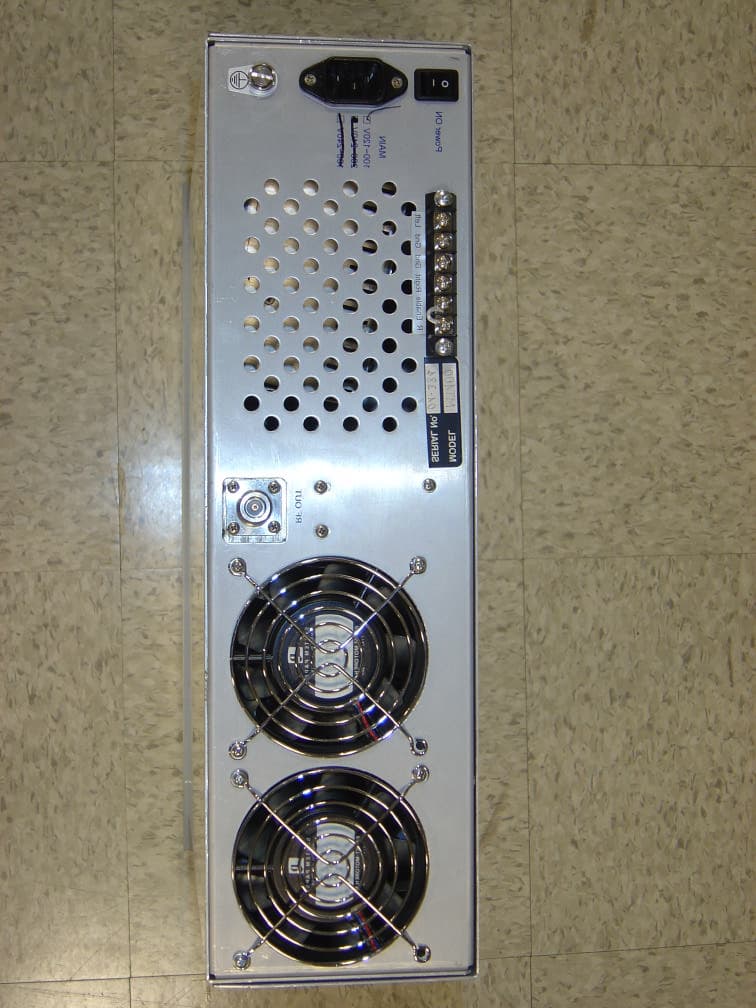
Click to zoom
Application Details
- Equipment Class
- TBC - Licensed Broadcast Station Transmitter
- Date of Grant
- Jul 07, 2004
- Application Purpose
- Original Equipment
- Date of Application
- Jul 07, 2004
- Equipment Note
- 100 Watt FM Transmitter
- Frequency Range
- 88.00000000 - 108.00000000
- Company
- Richardson Electronics Ltd
- Country
- United States
Documents & Files
Document Text
Text extracted from the exhibit documents filed with the FCC. Open a document above to read the original.
Users Manual
RFCAST – MT100. Rev. 2: 06-12-04 1/16 OWNERS MANUAL Model MT100 (-E & -U) 100 WATT FM STEREO TRANSMITTER RFCAST – MT100. Rev. 2: 06-12-04 2/16 USER NOTICES IT IS VERY IMPORTANT TO READ THE FOLLOWING MANUAL SECTIONS PRIOR TO OPERATION OF THIS TRANSMITTER! Notice 1 The transmitter main operating voltage setting is marked on the rear of the MT100 chassis. It may be necessary to change this setting for your operating condition. Please refer to AC Main Voltage Setting in section 6.0 Set Up Procedure. Notice 2 The transmitter operating frequency from the factory may not be set for your authorized frequency as it is normally set for a mid band value such as 98.0 MHz. Please refer to Frequency Of Operation Change in section 6.0 Set Up Procedure. Notice 3 For adjusting the RF output power setting a qualified technician should employ the use of an RF Wattmeter and a calibrated dummy load. Please refer to the section entitled RF Power Control in section 3.4 of this manual. Notice 4 The factory settings of this manual for such this as Input Selection, preemphasis, and input sensitivity may not be correct for your application or installation requirements. Please refer to the other exciter settings in section 6.0 Set Up Procedure where you will be directed where else to reference in this manual. GENERAL COMMENTS THIS PRODUCT DOES NOT INCLUDE A DETAILED TECHNICAL MANUAL, RATHER AN ENHANCED OPERATORS MANUAL. WHAT THIS DOCUMENTATION IS INTENDED TO DO IS TO GIVE THE USER THE CORRECT INSTRUCTIONS AND INDICATIONS ABOUT HOW TO OPERATE AND PERFORM PERIODIC CHECKS AND DETERMINE IF THE TRANSMITTER IS FUNCTIONING PROPERLY. WE ARE AWARE THAT THE TRANSMITTER DOCUMENTATION MAY PRESENT SOME SMALL AMBIGUITIES AND IMPERFECTIONS, MANY OF WHICH HAVE ALREADY BEEN NOTED AND RESOLVED IN THE NEXT RELEASE AND PRODUCTION. FOR THIS REASON, EVERY OBSERVATIONS/SUGGESTIONS OR PARTICULAR COMMENTS ARE WELCOME. RFCAST – MT100. Rev. 2: 06-12-04 3/16 ELECTRONIC FILES OF THE SCHEMATIC DIAGRAMS IN THIS MANUAL ARE AVAILABLE. SHOULD A LARGER MORE VIEWABLE VERSION OF ANY DIAGRAM BE REQUIRED NOTIFY RICHARDSON ELECTRONICS, LTD. TO CALL OUR TECHNICAL SUPPORT CENTER OR FOR OTHER CUSTOMER SERVICE ISSUES AT RICHARDSON ELECTRONICS IN LA FOX, ILLINOIS REFER TO THE FOLLOWING NUMBERS: TECHNICAL SUPPORT: 630-208-2790 CUSTOMER SERVICE: 630-208-2304 RFCAST – MT100. Rev. 2: 06-12-04 4/16 Returns and Exchanges Equipment (Damaged or undamaged) should not be returned unless written approval and a Merchandise Return Authorization (MRA Number) is received from your Richardson Sales representative or Richardson Customer Service. Special shipping instruction will be provided which will assure proper handling. The circumstances and reasons for the return must be included in the request for return. Equipment that is special or “custom” ordered may be not returnable. In situations where return or exchange is at the request of the customer a restocking fee may be charged. All returns must be sent freight prepaid and properly insured by customer. When communicating with Broadcast Richardson please refer to your Order or Invoice Number. Unpacking Use care when unpacking the equipment. First perform a visual inspection of the item(s) to determine if any damage occurred during shipment. Be sure to retain all the shipping materials (crates and boxes or cartons) until such time that it has been determined that the received equipment arrived undamaged. Find all PACKING LISTS and keep them to assist in locating and identifying any components or assemblies that may have been removed for shipping and might need to be reinstalled in the equipment. Make sure that all shipping straps, supports and packing materials are completely removed from the equipment prior to initialization and use. Technical Support Should you need technical assistance or trouble shooting guidance contact Broadcast Richardson in your local area or you can reach assistance from Broadcast Richardson in La Fox, Illinois at telephone +1 (630) 208-2782, Fax +1 (630) 208-2551 or Customer Service at +1 630-208-2304. Throughout the world there are many Richardson Electronics, Ltd. offices that are also able to assist in contacting our technical support team. RFCAST – MT100. Rev. 2: 06-12-04 5/16 WARNING! THE VOLTAGES AND CURRENTS IN THIS EQUIPMENT ARE DANGEROUS. PERSONEL MUST, AT ALL TIMES, OBSERVE SAFETY WARNINGS, INSTRUCTIONS, AND ANY REGULATIONS. This owner’s manual is intended as a general guide for trained and qualified personnel who are aware of the dangers that are inherent in the handling and operation of potentially hazardous electrical and electronic circuits. It is not the intent of this manual to provide a complete set of safety instructions or precautions that should already be understood by trained or experienced personnel in using this or other types of electronic equipment. The installation, operation, and maintenance of this equipment involves risks to personnel and also to the equipment. Broadcast Richardson or Richardson Electronics, Ltd. shall not be responsible for injury or damage that is the result of improper procedures or use by persons improperly trained or lacking the knowledge to perform associated tasks. All local codes for building, safety, fire, or related standards must be observed. Consult local authorities for the standards for the area or region where the equipment will be installed and put in use. WARNING! AT ALL TIMES DISCONECT AC/MAINS POWER BEFORE OPENING COVERS, DOORS, ENCLOSURES, PANELS, OR PROTECTIVE SHIELDS THAT EXPOSE LIVE CIRCUITS. USE ANY GROUNDING STICKS OR OTHER SHORTING PROBES TO DRAIN ENERGY FROM CIRCUITS BEFORE SERVICING. NEVER PERFORM MAINTENANCE, MAKE ADJUSTMENTS, OR SERVICE THE EQUIPMENT WHEN ALONE OR FATIGUED. WARNING! IF ELECTROLYTIC OR OIL FILLED CAPACITORS ARE UTILIZED IN THE EQUIPMENT AND THE COMPONENT APPEARS LEAKY, OR IS BULGING, OR IF THE CASE OR COVERING OF THE COMPONENT APPEARS DAMAGED OR DISTRESSED ALLOW SUFFICIENT TIME FOR THE UNIT TO COOL OR FUL…
Text truncated - open the document above for the full version.
Block Diagram
FANS FUSE 28 Vdc -V +V LED (DISPLAY) ENABLE 110 or 220Vac L.P.F. π Delay line RF out LOW PASS FILTER andDIRECTIONAL COUPLER RF AMPLIFIER SECTION REFL1 REFL2 FWD RF PROTECTION TEMPERATURE RF CONTROL CIRCUIT RF Monitor AC/DC CONVERTER DC/DC CONVERTER 28 Vin 28 Vdc 15 Vdc FANs EXTERNAL ENABLE OME-1T FM Exciter RFout 1Wmax Left Rigth Ext/MPX SCA/RDS AUX +15Vdc FINALSTAGE DRIVERSTAGE Not Used M T100 Block D iagr am
Operational Description
The MT100 RF Module, Final Power Stage The RF amplifier section provides to amplify the RF signal coming from the RF control circuit. It is composed by: • 2 way 90 deg. hybrid splitter • driver stage • final stage • 2 way 90 deg. hybrid combiner The 2way splitter is made by a 90 deg. Hybrid structure and provides to split in quadrature the input signal. Below, the technical specifications: Frequency 87.5 – 108 MHz Input power 50W Max Return Loss (S11) <-17 dB Return Loss (S22 ed S33) <-15 dB Isolation (S32) >15 dB Insertion Loss (S21=S31) <0.6 dB The driver stage provides the first step of amplification of minimum 14dB gain in order to correctly drive the final stages. It is composed by a pair of SINGLE END stages operating in class AB. Below, the technical specifications: VCC 28V Idq 50 mA per section Frequency range FM ( 87.5-108 MHz ) Gain > 16 dB typ. Output Power > 5 W The final stage is an amplifier stage for FM signal operating in band II (87.5 – 108 MHz), with nominal output power of 100 Watt CW. Normally it works up to 150 Watt, in order to win the Insertion loss of the circuitry that follows the amplifiers, as the 2 Way Combiner, Directional couplers, and Low Pass Filter. It is a balanced amplifier, including a pair of “push – pull” sections, each one using a medium power MOSFET with the input / output matching network, and balancing to unbalancing transformer (balun). The RF MOSFET‘s bias are integrated on this printed circuit board. The polarization is in class B, with a 25 mA quiescent current per section. VCC 28V IDC (@ Full Power) 7 A typ. Idq (total per 2 sections) 50 mA typ. Frequency range FM ( 87.5-108 MHz ) Power Gain > 17 dB typ. Output Power > 100 W The 2 way Combiner is a 2 way in quadrature structure, and it provides to sum each two final stage sections to have 250 W power at the common port. One unbalancing 50 Ohm resistor warranties the isolation between the input ports, in order to maintain the Transmitter on duty, in case one of the final stages will be on fault (- 6dB derating). Below, the technical specifications: Frequency 87.5 – 108 MHz Power handling 400 W Max Return Loss (S11) <18 dB Return Loss (S22 ed S33) <18 dB Isolation (S32) >18 dB Insertion Loss (S21=S31) < 0.4 dB
Parts List/Tune Up Info
MT100 STEREO LOW POWER FM TRANSMITTER 100 WATT 1.0 OVERVIEW MT100 is a 100 Watt FM Low Power Transmitter. It is very simple and easy to use. It is composed of a mechanical frame (19 inches std., 3 RU high and 500mm depth), an exciter (OME-1T), a RF section, which comprises a RF control board and an amplifier section, a directional coupler and a low pass filter, a display, a power supply with a AC/DC converter and a DC/DC converter. 2.0 MT100 BASIC BLOCK DIAGRAM FANS FUSE 28 Vdc -V +V LED (DISPLAY) ENABLE 110 or 220Vac L.P.F. Delay line RF out LOW PASS FILTER and DIRECTIONAL COUPLER RF AMPLIFIER SECTION REFL1 REFL2 FWD RF PROTECTION TEMPERATURE RF CONTROL CIRCUIT RF Monitor AC/DC CONVERTER DC/DC CONVERTER 2 8 V i n 2 8 V d c 1 5 V d c F A N s EXTERNAL ENABLE OME-1T FM Exciter RFout 1Wmax Left Rigth Ext/MPX SCA/RDS AUX +15Vdc FINAL STAGE DRIVER STAGE N o t U s e d 3.0 SUBASSEMBLIES DESCRIPTION 3.1 MT100 AC/DC Power Supply The AC/DC power supply is a vendor-supplied product. The input voltage is manually selectable for 220V or 110V, while the regulation range of the output voltage is 28V. The input voltage selector switch is located on the front of the power supply inside the MT100 chassis. The VADJ control is used to stabilize the output power. Below, are the power supply technical specifications: Input 110 Vac or 220 +/- 15% (manually switched) Output 28 to 30 Vdc I max 10 A operating; 15 A short circuit Efficiency 85% typ. Isolation 4 KV (In/out or In/GND) Weight (Typ.) 1500 g Size (WxHxD) 120x80x200 3.2 MT100 DC/DC Power Supply The MT100 uses a DC/DC converter. It provides a voltage of 15V to the exciter and power to the fan circuits. Below, the technical specifications: Vdc Input 20 up to 53 Vdc Output 1 15 Vdc/1.5 A Output 2 28 Vdc/3 A 3.3 FM Stereo Exciter The exciter is RFCast model OME-1T. The declared nominal RF output power is 1 Watt; this signal arrives to the RF final stage through the RF protection circuit. All the input connections are arranged on the front panel. Please refer to the annex datasheet at the back of this manual for more detailed specifications and for operational settings. 3.4 MT100 RF Control Circuit The RF input circuit has 3 main functions: 1) RF power control 2) RF protection 3) Measurement/status indication RF Power Control. A pin diode attenuator controls the RF input power coming from the exciter (OME-1T). RT3 trimmer may manually control this attenuator located on the internal control panel, in order to adjust for the output power requirement. The AGC control regulates the power, manually set, versus frequency and/or temperature changes. Moreover, the input attenuator includes a soft start, activated at the switching on or after any RF protection intervention. To access RT3 the operator engineer will need to remove the transmitter top cover. When the MT100 works at a very high temperature and/or high reflected output power, a derating circuit is provided to decrease the output power in order to allow the equipment on function at a reduced power. RF Protection. A fast comparator switches when the output detected reflected power exceeds a pre-set threshold. The regulation of this threshold is made by RT2 trimmer, adjusted in factory for a value of 20 Watts. When the protection is switched on, the protection circuitry removes the RF signal applied to the final stage amplifier very quickly, in about 1 microsecond. Measurement/status indication. The two main measurements, FWD and REF power, are displayed by two BAR LEDs. The MT100 status is indicated with 3 LED's: RF nominal, RF fault, RF derating. The RF fault is on when the output power is lower than 3 dB related to the nominal output power. If the power decreases in derating conditions, the fault is off in all cases. The “enable” switch (SW1) is located on the front panel. It is possible to operate the enable switch by using the contacts on the rear chassis panel of MT100. The enable mode of the amplifier is realized when switch SW1 is on and the rear panel contacts (jumper) are closed. WARNING: with enable off, there is no RF out but all the internal circuits are powered (stand by condition). Remember to switch off the main on / off switch on the transmitter rear panel and remove the power cord before opening the top cover or operating any inside circuits. Operating with the transmitter cover removed also affects the proper cooling of the RF amplifier. 3.5 MT100 RF Amplifier The RF amplifier section provides to amplify the RF signal coming from the RF control circuit. It is composed by: • 2 way 90 deg. hybrid splitter • driver stage • final stage • 2 way 90 deg. hybrid combiner The 2way splitter is made by a 90 deg. Hybrid structure and provides to split in quadrature the input signal. Below, the technical specifications: Frequency 87.5 – 108 MHz Input power 50W Max Return Loss (S11) <-17 dB Return Loss (S22 ed S33) <-15 dB Isolation (S32) >15 dB Insertion Loss (S21=S31) <0.6 dB The driver stage provides the first step of amplification of minimum 14dB gain in order to correctly drive the final stages. It is composed by a pair of SINGLE END stages operating in class AB. Below are the technical specifications: VCC 28V Idq 50 mA per section Frequency range FM ( 87.5-108 MHz ) Gain > 16 dB typ. Output Power > 5 W The final stage is an amplifier stage for FM signal operating in band II (87.5 – 108 MHz), with nominal output power of 100 Watts CW. Normally, the amplifier operates up to 150 Watts in order to overcome the Insertion loss of the circuitry that follows the amplifiers, being the 2 Way Combiner, Directional couplers, and Low Pass Filter. It is a balanced amplifier, including a pair of “push – pull” sections, each one using a medium power MOSFET with input / output matching network, and balancing to unbalancing transformer (balun). The RF MOSFET‘s bias are integrated on this printed circuit board. The polarization is in class B, with a 25 mA quiescent current per section. VCC 28V IDC (@ Full Power) 7 A…
Text truncated - open the document above for the full version.
RF Exposure Info
MT100 ii WARNING: RF Hazard Information THE ANTENNA(S) USED FOR THIS TRANSMITTER MUST BE FIXED-MOUNTED ON OUTDOOR PERMANENT STRUCTURES. RF EXPOSURE COMPLIANCE IS ADDRESSED AT THE TIME OF LICENSING, AS REQUIRED BY THE RESPONSIBLE FCC BUREAU(S) INCLUDING ANTENNA CO-LOCATION REQUIREMENTS OF PARA. 1.1307(B)(3). WARNING! THE VOLTAGES AND CURRENTS IN THIS EQUIPMENT ARE DANGEROUS. PERSONNEL MUST, AT ALL TIMES, OBSERVE SAFETY WARNINGS, INSTRUCTIONS, AND ANY REGULATIONS. This owner’s manual is intended as a general guide for trained and qualified personnel who are aware of the dangers that are inherent in the handling and operation of potentially hazardous electrical and electronic circuits. It is not the intent of this manual to provide a complete set of safety instructions or precautions that should already be understood by trained or experienced personnel in using this or other types of electronic equipment. The installation, operation, and maintenance of this equipment involves risks to personnel and also to the equipment. Broadcast Richardson or Richardson Electronics, Ltd. shall not be responsible for injury or damage that is the result of improper procedures or use by persons improperly trained or lacking the knowledge to perform associated tasks. All local codes for building, safety, fire, or related standards must be observed. Consult local authorities for the standards for the area or region where the equipment will be installed and put in use. WARNING! AT ALL TIMES DISCONECT AC/MAINS POWER BEFORE OPENING COVERS, DOORS, ENCLOSURES, PANELS, OR PROTECTIVE SHIELDS THAT EXPOSE LIVE CIRCUITS. USE GROUNDING STICKS OR OTHER SHORTING PROBES TO DRAIN ENERGY FROM CIRCUITS BEFORE SERVICING. NEVER PERFORM MAINTENANCE, MAKE ADJUSTMENTS, OR SERVICE THE EQUIPMENT WHEN ALONE OR FATIGUED. MT100 iii WARNING! IF ELECTROLYTIC OR OIL FILLED CAPACITORS ARE UTILIZED IN THE EQUIPMENT AND THE COMPONENT APPEARS LEAKY, OR IS BULGING, OR IF THE CASE OR COVERING OF THE COMPONENT APPEARS DAMAGED OR DISTRESSED ALLOW SUFFICIENT TIME FOR THE UNIT TO COOL OR FULLY DISCHARGE BEFORE SERVICING. SERVICING HOT OR LEAKY CAPACITORS CAN CAUSE A RUPTURE OF THE CASE AND POSSIBLE INJURY. Should accident or injury occur, personnel engaged in the installation, operation, or service of the equipment should seek proper medical attention. It is advisable that such personnel have familiarity with first-aid practices.
Schematics
A A B B C C D D E E 44 33 22 11 x1MHz 16 1 F/64 Prescaler 14 x 47k Ingenium - Pianopoli - Italy 2 - Synthetizer Stereo Coder PMBT 2222A PMBT 2222A 3 "100MHz" 15Vcc VCO & Buffer 1-2=Stereo 2-3=Mono x10MHz 3 PMBT 2222A "Lock" x100kHz RF OUT Peak Detector Loop Filter Led Bar #B Indicator Phase Comparator L&R Input and Preemphasis + 1 Reference Oscillator Virtual Ground Limiter 12.8MHz 2 Led Bar #A Indicator RF Power Amplifier PMBT 2222A Audio Filter 4x BAT46 L Input Sensitivity 1-2 = 6..9 dBm 2-3 = 3..6 dBm 3-4 = 0..3 dBm 1234 2134 2134 213 1 2 3 Preemphasis 1-2 = 75 uSec 2-3 = Linear 3-4 = 50 uSec Sensitivity See Left Ch. Preemphasis See Left Ch. R Input 0..3dB Fine Adj. 0..3dB Fine Adj. RDS 0dBm AUX 0dBm Mpx Ext +3..+9 dBm Limiter 1-2 =On 2-3 =Off Input selector 1-2 = Ext Mpx/Mono 2-3 = Int. Mpx 1-2 = +50kHz 2-3 = 0 Sync 1 2 17T/ 0C315/ 3D0 "Limit" 1-2 = RF Inhibit 2-3 = Lock Detector Inh. No Jumper= Normal Operation MonoStereo 4 MPX Adj Input |JP6|JP5 Mono |1-2|2-3 Mpx Int |1-2|1-2 Mpx Ext |2-3|2-3 123 1 23 1 2 3 MPN10 MPN10 A3 11 Wednesday, September 29, 1999 00 SE99012.DSN SizeDocument NumberRev Date:Sheetof App.DateApp.Sig.Dwg.Sig.Dwg. Date P7V5 P15V P7V5 P15V P15V P15V P15V P15V P7V5 P7V5 P7V5 P15V P15V P15V P15V P15V P15V P15V P15V P15V P15V P15V P15V P15V P15V P15V P7V5 P7V5 P7V5 LD13 Red R21 2k2 C76 100n R64 470k R125 2M2 R126 R109 2M2 C77 470p R119 Q4 BFR96S Q10 BC807 R143 1M0 R52 220 JP9 +- IC13A LM339 54 2 312 R43 470 L3 150n C32 220p2% C17 4p7 R29 2k2 R3 150 TP5 LD6 Green R138 C43 470p L8 150n R7533k R57 10R L1 R30 47R R814k7 DV6 BB153 R135 1k0 R114 47R T2 13 4 25 R27 1k8 T1 13 4 25 R324k7 C10 220n D10LL4148 C79 100u 35V C58 47p C57100p R11R0 C28 10n 2% R15 470k D16 LL4148 C4 2n2 C91 47p R176 470 C2 100n R10418k C74100n R155 2k2 CV1 5-20p D3 LL4148 R50 1k0 R161 6k8 H3 TCXO 1 2 3 Vdd Out Gnd R35 1k8 JP10 D4 LL4148 C5 10n 2% Vss IC10B 40107B 6 57 4 C20100p R89 TBD +- IC14D LM339 1110 13 Q6 BC817 R5633k JP1 L14 1T/0C5/3D0 Q7 BC807 IC8 SAB6456A 26 4 5 3 8 79 R68 150 D1 LL4148 R103 820 R6533k R145 10k LD4 Green JP7 D7 LL4148 CN4 +- IC13C LM339 98 14 R170TBD D9 SW3 321 5 4 BCD Com A JP2 R1746k8 IC5A 4027B 61 3 52 7 48 16 JQ CLK KQ S RVss Vdd JP6 C84 100n R19 1k8 R106 33k C86 10u 35V R13 150 +- IC13D LM339 1110 13 RT4 1k0 C49 2n2 C102 100n C94100n C15 6p8 R159 6k8 C39 47p R151 10k RT1 5k0 R428k2 R2 10k C44 47p LD7 Green R110 220 CN2 R121 2k2 CN1 C7 100n DZ1 9V1 C27 2n2 C53 470n R100 2k2 R882k C2910u25V Q19 BC807 R84 4k7 D12 C72 10u 35V R96 560 C100 10u 35V R1893k3 R2027k C65 100n C75 10u 35V C78 22n R123 2M2 L9 150n LD9 Red H2CTC30_01 1413121110987654321 27262524232221201918171615 m/sCTGndSync1216kGndGndLLeft inGndVssGndRight inR MPU 19k in CR CL Comp RComp C GndGnd C int MPX Vdd 19k out C trim R94 560 C70 100n R169 680 L20 Bead Neosid XT1 6400k Q17 BC817 C1 100u 35V R45 1M0 C87 47p R79 560 CN5 C83 100n C48 470p IC5B 4027B 1015 13 1114 9 12 JQ CLK KQ S R L11 220n R636k8 R51 22k CN8 C85 470n R191TBD R162 6k8 R80 1k0 C33 100n J3 BNC R556k8 L10 3u3 C50 100u 35V R177 10k R1576k8 C13 2n2 R168 3k3 C21 10u 35V R17 1M0 C59 10u 35V L12 180n C31 100n R12 10R C41 TBD C37 100u 63V C63 100n SW2 321 5 4 BCD Com A TP4 Q14 BC807 IC2A TL072 2 3 8 4 1 CN7 LD11 Green C12 100u 35V R173 470 C25 10u 35V R28 6k8 R40 150 R93 10R R147 470k DZ4 5V1 R172 10k DZ8 5V1 R77 2k2 Q12 BC817 C16 6p8 C24 10u 35V IC3A TL072 2 3 8 4 1 Q20 IC7B LM833 6 5 7 R6710k R113 1k8 R134 L15 150n IC4A OP275 2 3 1 IC9A 4027B 61 3 52 7 48 16 JQ CLK KQ S RVss Vdd R16 820 Q16 CN11 R5433k J5 R182 1k0 R166220 C30 10u 35V H1 FTC30_01 10987654321 16151413121117181920 Input A GndGnd -Vs GndGnd Output A GndGnd +Vs GndGndOutput BGndGnd+Vs-VsGndGndinput B IC4B OP275 6 5 7 R7610k SW1 321 5 4 BCD Com A L16 1u0 D6 LL4148 R41 22k R921M0 CN3 IC9B 4027B 1015 13 1114 9 12 JQ CLK KQ S R R610R R137 470k R2322k DV4 BB153 C101 2n2 J1 BNC C3 100n R108 2M2 TP3 R66 100 1W0 R59 6k8 DZ6 3V9 R122 2M2 C98 10u 35V D11 R105 33k C6 100n R911M0 IC7A LM833 2 3 1 R85 82k D13 JP5 R117 2k2 C67 2n2 R129 C80 100p L2 150n Q1 2 31 R190 1k0 LD3 Green R183 22R R181 33k LD10 Green R118 2k2 R180 33k R131 R5 4k7 R128 47k DZ2 3V9 LD2 Red R132 Q2 2 31 C60 1p0 R73 150 LD8 Yellow R98 82k R9 270 R4 47R R87 470k DZ3 3V9 C9 220p 2% R187150 R10 820 L5 DV1 BB153 C38 100u 35V C18 2n2 R163 6k8 R160 6k8 R78470 C69470n IC11A LM358 2 3 8 4 1 Vss IC10A 40107B 2 31 J4 R186 39R R33 47R DV2 BB153 C55 100n CN12 C34 100n R4627k CN10 R167 150 R185 150 +- IC14B LM339 76 1 DV3 BB153 C19 470p CN14 C54 10u 35V C81 100n JP8 R38 820 R60 47k L4 150n RT2 5k0 C97 10u 35V C71 10u 35V R31 10k R3647k R144 10k D15 R112 2k2 L7 2T/0C5/3D0 R39 220 R25 82k C62 15p C35 100n Q11 BC817 R10110k R175 10k C45 22n R37 270 R111 22k C96 470n R34 1M0 R49 1k0 C64 22n R47 2k2 R53 1k8 IC11B LM358 6 5 7 IC1 LM723 5 4 2 3 137 12 10 911 6 Pos In Neg In ILim ISen CompGnd Pwr Vout VZVC Vref IC6 4059B 345622212019181716151098712141311 231224 J1J2J3J4J5J6J7J8J9J10J11J12J13J14J15J16CLKLENKAKBKC NOUT VSSVCC R70 2k2 R188 3k3 J7 BNC R44 68R R133 R8822k L19 470n R901M0 C73 100n C90 47p +- IC14C LM339 98 14 R71 82k C40 6p8 C42 1p0 R61 47k R82 22R R136 R102 10k C36 2n2 R241M0 CN13 JP4 LD1 Green JP3 D14 C92 100n IC2B TL072 6 5 7 +- IC14A LM339 54 2 312 C89 470n R146 2k2 LD12 Yellow R171 560 R116 22R R139 470k J6 IC3B TL072 6 5 7 R62470 TP2 R127 47R R154 220k C68 470n DZ5 3V9 C51 2n2 C99 22n R178 1k0 CN9 L131u0 TP1 C14 470p CN15 R156 220k L18 220n C52 22n Q13 BC807 C82 100u 35V R164 6k8 R18 330 C11 47p R142 R95 560 C47 470p R165 6k8 Q21 BC807 C56 560p Q18 BC807 R22 1k8 C93 10u 35V L6 22u R149 18k L17150n R8333k C23 1u0 63V C88 470n Led Circuit Board R140 C8 100n +- IC13B LM339 76 1 D8 J2 BNC RT5 5k0 C46 22n R69 TBD R150 2k2 Q9 C61 8p2 R141 R179 10k R115 1k0 C22 1u0 63V CN6 DZ7 3V9 R48 2k2 IC12 4060B 1112 7546141315123910 8 PIRST Q4Q5Q6Q7Q8Q9 Q10Q12Q13Q14 POPO VSS R26 6k8 R130 22k LD5 Red R99 82k C66 2n2 DV5 BB153 R184 82k R148 18k C95 2n2 R74 39R RT3 10k Q22 BC817 R158 5M6 R97 470 R120 R58 470 Q8 D17 LL4148 R107 22k R86 82k Q5 BFG135 R148k2 Q3 …
Text truncated - open the document above for the full version.
Schematics
5 5 4 4 3 3 2 2 1 1 DD CC BB AA ANAREN 1-H0280-3 GR00201BSE.DSN B MT100 INGENIUM A3 11Thursday, January 31, 2002 Title SizeDocument NumberRev Date:Sheetof DWG.Sig.Dwg. DateApp.Sig.App.Date RF OUT RF IN ENABLE1 Vdd Vdd VD1 ENABLE1 VD2 Vdd VD1 VD2 TEMPERATURE SENSOR R10 22R Q4 D1018UK 3 41 2 6 5 L14 5T0/0C5/3D5 R18 2k2 C12 47n C47 1n0 H1 L10 1u0 R3 1R0 C21 1n0 L6 4T0/0C2/R10R35 22R 2W0 C19 1n0 C40 47n C1 47n C22 470p L9 4T0/0C2/ su R24 C20 470p C45 27p L1 1u0 R5 68R R8 2k2 L5 5T0/0C5/3D5 R11 100 R16 2k2 C39 4n7 Q2 Q2 D1083UK 2 31 R40 220 C4 47n C8 150p R41 220 Q5 Q5 D1083UK 2 31 D5 BAS16 C17 27p C48 470p ATC C15 150p C43 150p R34 680 C11 4n7 C16 470p ATC C5 1n0 R6 680 C38 TBD TR2 30 CM RG316-BU 50R + FB2 C37 4n7 100V C7 470p ATC L12 3T0/0C8/4D0 C6 1n0 C9 4n7 100V C35 470p ATC L18 6T0/0C8/SU R36 R13 50R 60W L13 4T0/0C5/3D0 H2 C49 100u 35V 1 2 C2 4u7 35V 1 2 C44 470p ATC R1 2k2 C42 18p C10 TBD RT1 10k L4 4T0/0C5/3D0 TR3 20 CM RG316-BU 50R + FB3 D1 BAS32 C14 18p R29 2k2 R9 2k2 R33 68R C3 47n R32 10R R7 1k0 C32 47n TR1 20 CM RG316-BU 50R + FB1 C18 47n C36 150p DZ3 9V1 C31 47n R42 10k NTC L2 220n D4 BAS16 DZ2 15V Q1 D1018UK 3 41 2 6 5 DZ4 6V8 RT4 10k R12 1k8 L3 3T0/0C8/4D0 L17 6T0/0C8/SU R35 R26 10k D6 BAS32 R14 68R R15 1k8 RT2 10k C30 4u7 35V 1 2 R20 68k C51 1n0 C27 1n0 R27 10k R25 10k R4 10R C52 1n0 C50 100u 35V 1 2 D2 BAS16 RT3 10k R30 12k C24 1n0 C28 470p C41 1n0 C23 1n0 DZ5 15V C25 470p C59 1n0 R23 2k2 C46 470p ATC R21 100 R2 12k C29 47n R22 2k2 C53 27p ATC R24 22R R19 22R D3 BAS16 C54 22p ATC L11 220n C55 27p ATC R28 51R 1W0 L7 4T0/0C2/ su R19 C56 22p ATC C33 1n0 C57 10p ATC C58 6p8 ATC C34 1n0 C26 1n0 C60 10p ATC R17 22R R31 1R0 L15 1T0/1C1 SU FB08 R38 0R0 L16 1T0/1C1 SU FB08 R36 22R 2W0 L8 4T0/0C2/R17 TR4 30 CM RG316-BU 50R + FB4 DZ1 15V Q3 BC807 R39 0R0
Schematics
5 5 4 4 3 3 2 2 1 1 DD CC BB AA Refl Threshold DERATINGRF NOMINALFAULT Refl. Level Setting ENABLE MAIN 7- Refl2 1- V_ADJ CN1 pins description function 3- REfl1 2- GND 10- +15V 6- Main_Led 4-T_Sensor 5- FWD 9- +15V 8- GND lefty lefty right right Forward Power Reflected Power 5k 5k Power Control GR00221ASE C LOGIC CONTROL BOARD MT100 INGENIUM A3 11Friday, January 25, 2002 Title SizeDocument NumberRev Date:Sheet of DWG.Sig.Dwg. DateApp.Sig.App.Date +15V +15V +15V RF INPUT +10V +15V +10V +10V +15V +15V +15V +15V +15V +10V+10V +10V+15V +10V +10V +10V +15V +15V+15V +15V 10k R72 100n C19 BAT46 D10 270 R31 D16 BAT46 6k8 R86 470p C24 390 R82 RT1 5k0 1 3 2 BAT46 D13 2k2 R71 100n C9 C36 100u 25V 1 2 BC817 Q1 1 2 3 BAT46 D6 LD19 LED 12k R87 220p C4 10k R20 22p C13 1k0 R41 100k R75 IC6A LM358 2 3 8 4 1 IC5A LM358 2 3 8 4 1 10kR39 220p C11 100n C29 2V7 DZ5 33k R89 1k0 R35 220p C53 IC1LM3916 1 2 3 4 5 6 7 8 910 11 12 13 14 15 16 17 18 1 2 3 4 5 6 7 8 910 11 12 13 14 15 16 17 18 220k R45 220p C6 IC8B LM358 6 5 7 + - LM311 U1 2 3 4 1 7 85 6 IC4LM3916 1 2 3 4 5 6 7 8 910 11 12 13 14 15 16 17 18 1 2 3 4 5 6 7 8 910 11 12 13 14 15 16 17 18 2V7 DZ3 C35 10u 25V 1 2 HSMP3810 D1 LD2 LED 270 R23 470 R59 220p C5 100n C25 CN2 BARST M2 D18 BAT46 HSMP3810 D2 CONFLAT_10 CN1 12345678910 330 R34 LD3 LED BAT46 D5 RT3 1 3 2 22p C22 5k6 R26 HSMP3810 D3 xx R47 39k R84 10u L2 LD4 LED 1k0 R96 100u C32 1 2 2k2 R76 680 R58 390 R50 LD15 LED 470p C44 4k7 R93 4k7 R88 BC817 Q2 1 23 470 R64 100n C48 LD5 LED 22p C49 3k9 R70 12k R77 33k R30 390 R48 100n C50 9V1 DZ1 2 1 470 R67 2k2 R14 LD6 LED 12k R100 330 R28 5k0 RT2 13 2 9V1 DZ2 470p C47 10u C28 1 2 220p C14 LD17 LED BAT46 D7 10u L1 LD7 LED 2V7 DZ4 470p C1 LD8 LED 470p C42 100n C37 8k2 R95 220p C15 680 R49 LD11 LED 470p C46 22p C43 3k9 R68 51R 1W0 R3 LD9 LED 10u C17 1 2 22p C41 220p C16 BAT46 D17 2k2 R60 IC3B LM358 6 5 7 1n C20 0R0 DZ7BAS16 D24 22p C45 IC7B LM358 6 5 7 1k0 R42 470p C2 51R 1W R7 LD10 LED 9V1 DZ10 470p C40 2k7 R17 12k R81 9V1 DZ6 1k0 R22 330k R92 D20 RA-LED LD13 LED 2k2 R24 220k R32 LD1 LED 12kR46 100n C27 4k7 R13 D22 RA-LED LD14 LED IC3A LM358 2 3 8 4 1 10k R61 IC6B LM358 6 5 7 SW1 SW KEY-Y1011 1 23 IC7A LM358 2 3 8 4 1 470p C8 IC5B LM358 6 5 7 D21 RA-LED 1k0 R63 6k8 R97 LD18 LED BAT46 D8 470 R66 6k8 R54 100n C3 51 1WR44 D19 RA-LED 6k8 R37 xx R53 220p C10 4k7 R27 D15 BAT46 680 R55 4k7 R25 51 1WR43 4k7 R101 100n C34 xx R83 4k7 R91 100n C51 470p C7 4k7 R65 3k3 R36 100 R10 100n C26 220p C21 D14 BAT46 xx R11 100n C38 SW277 IC2 3 5 76 8 2 14 3 5 76 8 2 14 8k2 R62 CN3 C54 470u 35V 1 2 22p C18 3k9R38 10u L3470 R8 12k R73 J1 1 2 BAT46 D11 5k6 R51 LD20 LED 220 R18 220p C52 100 R9 51 1WR1 470p C39 LD12 LED 220 R15 1k0 R90 10k R16 22 R4 51 1WR2 150k R74 33k R85 10k R40 12k R69 100n C33 Q13 BC807 xx R6 RT1 1 3 2 2k2 R57 12k R80 10k R12 10k R94 100 R78 390 R19 BAT46 D9 100u C23 1 2 220 R33 BC817 Q3 1 2 3 470p C31 IC8A LM358 2 3 8 4 1 22k R79 220 R99 BC817 Q12 1 2 3 56k R98 BAT46 D4 4k7 R5 LD16 LED 100n C12 10u C30 12 33 R29 10k R52 6k8 R56
Schematics
5 5 4 4 3 3 2 2 1 1 DD CC BB AA GR00175ASEA GR00175 - 250W Low Pass Filter A4 22Monday, November 26, 2001 INGENIUM Title SizeDocument NumberRev Date:Sheet of DWG.Sig.Dwg. DateApp.Sig.App.Date C19 1p2 C17 12p L4 2T0/2C0/18D0 C2 1p2 C16 15p CN1 C18 1p2 SOLDER_POINT1 C1 1p2 CC1 300 mm RG316/25ohm su Balun core FB.... 12 C6 15p C7 15p C4 12p C8 15p L1 2T0/2C0/18D0 L2 2T0/2C0/16D5 C5 15p C10 6p8 L3 2T0/2C0/16D5 C11 15p C12 15p C14 15p C3 12p C13 15p C15 15p
Schematics
5 5 4 4 3 3 2 2 1 1 DD CC BB AA 2x GR00219ASEC 100W Directional Coupler A4 11Tuesday, February 12, 2002 INGENIUM Title SizeDocument NumberRev Date:Sheet of DWG.Sig.Dwg. DateApp.Sig.App.Date +15V +15V RF OUT (to Filter) R10 2k2 R12 2k2 RF IN CN1 R9 82R RT1 10k C7 12p H1 120 D2 MA4CS103A CC2 . . R2 560 D4 MA4CS103A C16 100p L3 47n L2 47n C10 100p D6 MA4CS103A C9 12p C22 100p R17 3k3 C19 100p C20 100p H2 R5 56 D1 MA4CS103A C3 2p2 R4 100 L4 47n C21 100p C6 68p R1 120 C11 100p R8 47R RF Monitor CN3 CN2 1 2 3 4 5 6 7 8 9 10 C17 100p R3 82R LM358 IC1 2 3 8 4 1 CC1 .. C13 100p C12 100p R18 180 R13 1k R11 2k2 D5 MA4CS103A L1 47n C8 6p8 R6 100 C14 100p C23 100p C24 100n D3 MA4CS103A R7 47R C4 68p R14 10k R16 10k C18 100n C5 82p L5 47n C15 100p R15 10k
Schematics
5 5 4 4 3 3 2 2 1 1 DD CC BB AA Supply Input 37 to 52V + V_ADJ - NC 8- GND 2- GND 7- Refl2 6- Main_Led CN5 pins description function 1- V_ADJ 10- +15V 9- +15V 4- T_Sensor From AC/DC 5- FWD 3- REfl1 Output 15.7V Nom. 1 +15V To FANS To Temp. Sensor 1 +28V 3- -28V CN4 pins description function 1- +28V 10- T_Sensor 9- GND 2- +28V 4- -28V 5- +28V 6- +28V 7- -28V 8- -28V GR00193BSE.DSNB DC/DC 90W Converter A4 11Tuesday, November 27, 2001 INGENIUM Title SizeDocument NumberRev Date:Sheet of DWG.Sig.Dwg. DateApp.Sig.App.Date A A R24 82K R4 1k5 C1 220u 55V 1 2 C18 100n R26 47k C12 100n R91k8 C41 100n CN5 1 2 3 4 5 6 7 8 9 10 C37 100n R20 47K L3 13T/Yellow Balun Core R18 4k7 CN6 C22 470n R19 1k C17 220u 35V 1 2 D4 ES2A 21 R51k8 C25 100n R7 10k CN1 L5 13T/Yellow Balun Core IC2B 6 5 7 CN2 R11 22kR12 22k L4 150u Q1 MTH35N15 2 31 R16 3M9 C38 100n C20 1000u 50V 1 2 R22 18k Q2 BC817 1 2 3 C26 100n C43 100n CN3 R1510k C19 1000u 50V 1 2 C44 100n …
Text truncated - open the document above for the full version.
Contact Information
Applicant
Peter Reinhard
630-208-2423Fax: 630-208-2551
Test Firm
Elite Electronic Engineering Co.Daniel Crowder
Technical Specifications
| # | Rule Parts | Frequency Range | Power Output | Emission | Tolerance |
|---|---|---|---|---|---|
| 2 | 73 | 88 MHz - 108 MHz | 100 W | 180KF8E | 40 Hz |
Other Applications from Richardson Electronics Ltd
NXHMT300
Jun 09, 2004300W FM Transmitter
Equipment Class
TBC - Licensed Broadcast Station Transmitter