O6E713050BVHF Fixed Station Transceiver
Midland Radio Corporation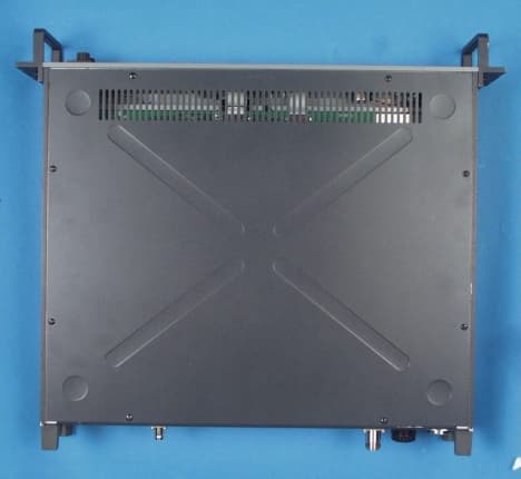
Click to zoom
Application Details
- Equipment Class
- TNB - Licensed Non-Broadcast Station Transmitter
- Date of Grant
- Dec 04, 2000
- Application Purpose
- Original Equipment
- Date of Application
- Dec 04, 2000
- Equipment Note
- VHF Fixed Station Transceiver
- Frequency Range
- 150.00000000 - 174.00000000
- Company
- Midland Radio Corporation
- Country
- United States
Documents & Files
Document Text
Text extracted from the exhibit documents filed with the FCC. Open a document above to read the original.
Users Manual
OPERATORS MANUAL KYODO KG510 BASE/REPEATER KYODO KG510 OPERATORS MANUAL 128194Page #2 of 26 Pages11 December, 2000 CONTENTS SECTIONDESCRIPTIONPAGE 1INTRODUCTION 4 2PRODUCT DESCRIPTION 4 2.1 Features 4 2.2 Product Description 4 2.3 Standard Inclusions 5 CONTROLS, INDICATORS, & CONNECTORS 5 3 3.1 Front Panel Controls5-7 3.2 Rear Panel Connectors7 OPERATION 4.1 Installation and Programming 8 4.2 Basic Operation8 4.2.1 Switch On 4.2.2 Adjust the Volume Setting 4.2.3 Adjust the Squelch Setting 4.2.4 Select the Channel 4.2.5 Receiving 4.2.6 Transmitting 8 8 8 8 8 8 4 4.3 Front Panel Operation 4.3.1 Keypad Operation 4.3.2 Keypad Operation using the SHIFT Key 4.3.3 Changing Channels 9 9 10 11 4.4 Signalling 11 4.4.1 5-Tone Signalling 11 4.4.1.1 Available Tones11 4.4.1.2 Entering 5-Tone Encoding Sequences 11 4.4.1.3 Recalling the Last Encode Sequence12 4.4 2 DTMF Signalling 12 4.4.2.1 Available Tones12 4.4.2.2 DTMF Tone Entry 12 KYODO KG510 OPERATORS MANUAL 128194Page #3 of 26 Pages11 December, 2000 CONTENTS SECTIONDESCRIPTIONPAGE 4.4.2.3 Redialling with DTMF 13 4.4.2.4 Restoring the Last DTMF Numbers to the LCD Display 13 4.4 3 Single Tone Encoding13 4.4.4 Kill Signalling 14 4.4.4.1 Kill Signalling Operation14 4.5 Channel Scanning 15 4.5.1 All Channel Scan Operation 15 4.5 2 Program Channel Scan Operation16 4.5.3 Exiting Scan Modes 16 4.5.4 Priority Scanning16 4.5.5 Removing Channels from Scan List 17 4.5.6 Restoring Channels to the Scan List17 4.6 Locking the Key Pad 17 4.7 Changing Tone Signalling Systems 18 4.8 Displaying Channel Information 18 4.9 Displaying Received Tone Frequencies 19 4.10 Bar Graph Displays 20 4.11 LCD Display Back Light 20 4.12 Transmit Power Change 20 4.13 Calling Party ID Display 21 4.14 Displaying any Radio's ID Number 21 4.15 Emergency Caller Display 22 4.16 Automatic Transmit in Repeater Mode 22 4.17 TX Test Mode 23 4.18 Key Pad Test Mode 23 4.19 Frequency Band Test Mode 24 4.20 Starting Message24 4.21 Serial Number Display25 4.22 EEPROM Data Check Mode25 4.23 Hardware Error Detection26 4.24 RS232C Communications Error Messages26 KYODO KG510 OPERATORS MANUAL 128194Page #4 of 26 Pages11 December, 2000 1.0INTRODUCTION Thank you for purchasing a KYODO KG510 Base or Repeater. We trust that it will operate reliably and give you years of service. If not, or if you wish to suggest ways of improving the KG510's operation, or features, we would welcome your comments. 2.0 FEATURES & PRODUCT DESCRIPTION 2.1Features ! Simplex or two frequency Duplex operation ! EEPROM programmable with a PC computer ! Single Channel and 99 Channel Versions available ! Full Dot Matrix Liquid Crystal Display ! All FM Frequency Bands from 30 to 520 MHz ! Front Facing Speaker ! Transmit Time Limiter to prevent channel jamming ! TX and RX Encryption ! Two Channel Scanning Modes ! 5 Tone Encoder & Decoder plus DTMF Encoder & Decoder ! 22, 26, or 35 MHz switching bandwidth (model dependant) ! Up to 99 channels with Channel Labels ! Two-Stage Front End allows mixed Simplex and Duplex operation ! Channel selectable Wide or Narrow channel spacing ! CTCSS/DCS on a per channel basis ! 5 X 4 Keypad for Channel Change etc ! 2RU Equipment Cabinet ! Step-Up VCO Voltage for Superior Selectivity ! Low Stand-by Current is ideal for Solar Installations ! Watch Dog Timer 2.2Product Description The Kyodo KG510 transceivers represent a quantum advance on the previous rugged & time proven KG110 transceiver. They comprise of separate modules all housed within one 2RU equipment cabinet. The receiver, the transmitter, and the PA Unit are each enclosed within their own diecast housing, that are then directly mounted on the large upper heat-sink. A μProcessor controlled interface module controls the channel selection, LCD Display, timers, interfaces, and signalling features. Models are available for all FM commercial and military frequency bands from 30 MHz to 520 MHz, with channel selectable 12.5, 20, 25, or 30KHz channel spacing arrangements. The RF Power Output is 1 - 50 Watts on a continuous duty basis. The CTCSS module supports all EIA tones. All tones and different encode and decode tones can be set on a per channel basis during radio programming. The KG510 includes 5 tone Selective Calling encoder/decoder with non-predictive decoder, as well as a DTMF encoder, and voice encryption. It supports normal all channel scanning and programmed channel scanning for base use. The KG510 is fitted with a large full dot matrix LCD that is used to display the Channel Numbers & Names, frequency & tone programmed information, and signalling information. All user interface keys and knobs are conveniently located on the front of the radio. All user entered functions are easily activated in a logical manner via the keypad. The KG510 is supplied with an "N" Type connector for the transmitter, and a TNC Connector for the Receiver to allow easy connection to the diplexer or feeder cables. The rear panel includes a 9 way D sub connector for fitment of an external shared tone panel. Also included is a 25 way D sub connector that enables external interface to other radios or control equipment. KYODO KG510 OPERATORS MANUAL 128194Page #5 of 26 Pages11 December, 2000 2.3 Standard Inclusions The KG510 transceiver is supplied complete with the following items: KG510 transceiver DC Cable Operators Manual KD561 Hand Microphone 3.0 CONTROLS, INDICATORS, & CONNECTORS 3.1 Front Panel Controls 1. 1.1. 1. Headphone Socket This socket is provided to allow users to listen to the KG510 using headphones. Plugging a headphone into this socket will disconnect the built-In speaker. It does NOT include a microphone input, or TX PTT facility. 2. 2.2. 2. High TX Power This is a service point and is not used by the radio operators 3. 3.3. 3. Low TX Power This is a service point and is not used by the radio operators 4. 4.4. 4. Loud Speaker* The receiver audio signals are heard from this speaker (provided that the volume setting is loud enough and provided that th…
Text truncated - open the document above for the full version.
Cover Letter(s)
Mr. Frank Coperich Re: FCC ID: 06E713050B; Securicor Wireless 731 Confirmation Number TC99431 Correspondence Reference Number 1115 Per referenced inquiry: 1. The transceiver uses PLL technology based on EPROM frequency selection. The EPROM can only be programmed by a programmer available only to authorized technicians. The equipment can only be operated on internally preset discrete frequencies authorized by applicable license. 2. Noted. Response from Hyak on 1/9/01 Gretchen Torres
External Photos
Front View Botto m View Left Side View Right Side View Rear View Top View
Internal Photos
Exciter Interior Interior Logic Interior Receiver Interior PA Interior
Operational Description
CIRCUITS TO SUPPRESS SPURIOUS RADIATION, LIMIT MODULATION AND CONTROL POWER 1) VCO section The oscillator circuit formed by L303, D305 and D306 generates transmitter frequencies. Then this signal is fed to the 3-stage of amplifiers, buffer amplifier Q302, pre,-ampufler IC301 and post amplifier Q303 and lead to the final amplifier. 2) PLL section Basically, the circuit description is the same as Rx. PLL IC inclusive with pre-scaller IC205 compares the phase between the VCO signal and reference oscillator frequency (12.00NMz) by method of dividing the frequency, and produces VCO control signal. Then this VCO control signal is fed to the charge pump, consisting of Q206, Q207 and Q208, and fed to the LPF. The supply voltage of charge pump is amplified by IC206 (approx. 15V) to achieve greater C/N ratio. 3) Modulator section The modulation signal is fed to both VCO and the reference oscillator (TCVXO), this permits a very flat modulation characteristics against low frequency (DC). This is the advantage when KG510 is used for POCSAG transmitter. 4) Tx younger section The VCO signal is amplified by Q215 and Q216 to achieve 250mW. But VHF bands (136-174MHz) has only stage of amplifier Q215 to achieve l00mW. 5) PA section The signal from younger stage is fed to PM510 and Q510 (VHF bands have no Q501) to achieve 50W output power. Then, signal is fed to the LPF to eliminate the harmonics spurious frequencies. An APC circuit formed by IC502, IC503, Q504 and Q505 stabilizes the output power at the set level. An IC501 protects PM501 and Q501 from the reverse power caused by the unmatched aerials. CIRCUITS TO SUPPRESS SPURIOUS RADIATION, LIMIT MODULATION- AND CONTROL POWER FCC ID: O6E713050B
Parts List/Tune Up Info
ALIGNMENT PROCEDURES KYODO KG510 BASE/REPEATER RECEIVER PART 1) BPF-1 and BPF-2 alignment Connect the signal generator to the Rx antenna connector of KG510. Align the BPF-1 and BPF-2 to obtain the maximum sensitivity. For better alignment, if yo u have spectr um a nal yzer a nd trac king ge nerator, co nnect the trac king ge ne- rator to the Rx antenna connector and pick up the output signal from J101 to connect spectrum analyzer. Align the BPF-1 and BPF-2 to have cover the desired bandwidth of receiving frequencies. 2) FVR101 alignment This is to adjust the squelch tihgt level. 3) VCO alignme nt Set the VCO voltage at 10.5V by L303 at the highest receiving frequency. TRANSMITTER PART 1) FVR201 alignment This potentiometer determines the modulation level. Carefully aling this potentiometer to obtain flat deviation from the lowest to the highest frequency installed n the transmitter. 2) FVR202 alignment This potentiometer determines the low frequency (below 300Hz) deviation. When POCSAG, CTCSS or DCS are used, necessary to align to have enough deviation at low freque nc y. 3) FVR203 alignment This potentiometer sets the maximum deviation, normally set at 5KHz. 2KHz or 2.5KHz deviation for narrow spacing can be set by programming software. 4) FVR204 alignment This is to adjust the transmitter output power. 5) VCO alignme nt Set the VCO voltage at 10.5V at the highest channel frequency. LOGIC PART 1) FVR1 alignment This potentiometer is to obtain 600 ohm 0dBm output of the RF signal. 2) FVR2 alignment This is to set the deviation level when KG510 is used for a repeater. 3) FVR3 alignment This is to set the Tx output power level indicating on the LCD. 1) FVC1 alignment This is to shift the CPU clock frequency when necessary. A beat interference sometimes happens at certain frequency. In such case, shifting the CPU clock frequency may eliminate the interference. FRONT CONTROL PANEL PART 1) VR401 alignment This is a volume controller. 2) VR402 alignment This is a squelch level controller. 3) FVR401 alignment This is to set the HI-POWER-LEVEL of the Tx output power. 4) FVR402 alignment This is to set the LO-POWER=LEVEL of the Tx output power. 5) FVR403 alignment This is to set the contrast of the LCD back light.
Schematics
2SC2412KQ504 FVR504 100K A M68702L C517PM1C516 4P 68P C536 1.5PC537R509 1P270ƒ¶ R546 4.7K 1KR545 ¦ R527 270ƒ¶ 1WR532 100KR533 1 2 3 M5237ML IC503 2.2KR548 R530100K 1SS355 D508 R52947K C551 ¦ 2KFVR503 4 1 23 BAM4558F IC501:A C5500.1ƒÊ D5071SS355 R526100K 100KR525 3 1 4 2 5 TA75S01F IC502 3.9KR523 1KR520 1 3 IC504 AN78L05M 470ƒ¶R513 10K R519 D506UDZ2.4B R517100K C547 1n 6.8K R518 R5145.6K 56 7 8 BAM4558F IC501:B 2KFVR502 C5460.22ƒÊ R515 47K C548 1n C5560.1ƒÊ 0.1ƒÊC553 270ƒ¶R531 12KR534 2.2ƒÊ/16VC555 33ƒÊ/25V C554 4.7KR535 2SB1018AQ505 1KR537 R502470ƒ¶ 1.8KR501 PWIN CN501 2SC1947Q501 D5011SS356 C5021n470PC501 R50656ƒ¶ 39PC517 C504150P C505 1n 150PC503 R5033.3ƒ¶ R507 1.5K 470ƒ¶ 1/8WR538 R544 4.7ƒ¶ 1/8W PM1 M68702H 0.29ƒÊL501 C514UC23 ¦ UC23C511 ¦ 470PUC34C513 C506 1n C512 150P C507 ¦ C508 1n C509 ¦ C510 1n 33ƒÊ/25V C552 5.6KR524 5.6KR522 C5491n FBA04.900BL518 4.7ƒ¶ 1/8W R528 BL515 FBA04.900 BL512FBA04.900 BL519FBA04.900 FC501IHB340 C5414.7ƒÊ C542 GRM40 0.01ƒÊ D509 1SS355 1K R521 2SK2731Q507 270ƒ¶R539 DTB143EKQ503 10KR512 R51010K Q502DTC124EKA 470KR516 180KR536 R51110K TP501RCT BL514FBA04.900 FBA04.900BL506 1nC527 1nC525 C5261n FBA04.900 BL505 RB501VD503 RB501V D504 HM501BL507 47ƒ¶R547 C5401n TP502RCT C515 UC23 ¦ C516UC23 ¦ C522UC23 ¦ ¦ C523 0.5P C521 D505 RB501V FVC505 ¦ C5281n C530 1n C529 1n L502 FVR501200ƒ¶ 150ƒ¶R509 C5241.5P BL509FBA04.900 L503 R546 ¦ ¦ C536UP050 C558UC233P C532 UC23 15P C531 820P UC34 HM501 BL508 C559UC2315P C533UC2318P R5402.7K SML-210VT D510 C5451n R542 4.7K 2.7K R543 R541 4.7K HM501BL510
Schematics
A 680ƒ¶R233 C2260.1ƒÊ BU4S66 IC207 4 352 1 UMC2NQ209 R227 27K R22947ƒ¶ 47ƒ¶R230 C2281.5ƒÊGRM42 D207:A DA204U D207:B 15n C218 2SK3018 Q208 47n C227 2SJ166 Q207 18K R228 1KR232 2SK3018Q206R2244.7K R2251KC256 22n C222 10ƒÊ 39K R231 R21312K 1ƒÊ C209 GRM42 2 5 3 1 4 UMC2NQ203 15nC220 6.8K R214 D2021SS355 MB1511 IC205 10KR215 10KR216 10KR217 0.22ƒÊC208 R20468K C204 100P 100KR210GRM421ƒÊC205 56 7 8 TS272CD IC203:B 4 23 1 TS272CD IC203:A ¦ C206 R21215K 100KFVR203 C207 47P TA75S01F IC204 R211180K FVR201 10K PW.CONT SIMP ERR REF VCO TCXO CK DATA LE TX.OUT TX2 R242 ¦ 16 15 14 13 12 11 10 4 5 6 7 8 9 3 2 1 CN202 FLC202 R23647K 2.7KR234 R28547K Q2172SK880 1M R286 100KR284 R21910K 10ƒÊ C224 1 6 CS201 C219 2.2ƒÊ/16V C229 ¦ C236470P D205 1SS355 IC206 NJU7662M R221 100K 100ƒ¶ R222 2SD2351Q205 4.7KR223 D206:A DA204U D206:B 10n C255 10ƒÊ C221 10ƒÊC223 10ƒÊ C225 V C O 12 CS202 R26410ƒ¶ R265270ƒ¶ 15PC240 10ƒÊ C213 10P C217 150PC215 47n C214 BLM21BL203 C211 47n BL206HM501 BL205BLM21 BLM21BL204 C212 10ƒÊ 1 3 IC201 AN78L05M 200KFVR202 15KR205 4.7KR206 4.7ƒÊ C202 R20710K C210 1n 100KR209 DC OUT GND V.C. 12.00MHzOSC201 2SB1184Q212 270ƒ¶R239 1 2 IC202 TA78M05F D201 UDZ2.4B C203 1ƒÊ 10ƒÊ C201 BL202HM501 BL201HM501 C257 1ƒÊ R244 47K Q214 IMX1 R 2 1 5 5KFVR204 R240470ƒ¶ 1/8W R1 R24615K 10KR241 10KR243 0.15ƒÊC230 C243 1n R270 470ƒ¶ L201:A#1091L201:B R2694.7ƒ¶ C242 ¦ R2674.7ƒ¶ 4.7KR268 1SS356 D212 C241 1n 2SC2954 Q215 150ƒ¶R266 C244 33P 10ƒ¶ 1/8W R271 C250 ¦ 33P C248 2.2ƒ¶R274 R2720ƒ¶ 1/8W C23933ƒÊ BL207BLM21 R2371.5K +12V GND +12V TX1 R235 ¦ R27710K R238 ¦ 1n C238 Q201DTC124EKA 10KR203 Q202 FMG9A FMG2AQ210 3 12 IC208 M5237ML C231 1n R20110K R20210K 10KR261
Schematics
R326470K ¦ R304 L30668nH 1 6 CP301 68K R303D303 1SV231 0.5P C306C307C308 10P33P A No C303 47P RCT TP301 C304 ¦ 82n C302 1SV232D303 D304 ¦ ¦ D302 0ƒ¶R305 1ƒÊHL301 ¦ R302 C307 8P R30147K R32447K GRM390.3PC306 D301 1SV239 R3031M 33P C303 D3051SV232 1SV239D306 L303#3073 C305 0ƒ¶ 27P C308 4.7K R309 C312 1n 56ƒ¶R306 470ƒ¶R311 R312100ƒ¶ C309 7P 0.82ƒÊL304 2SK508Q301 R3084.7K R310470ƒ¶ 1.5KR307 2.5PC311 C3105P TH301 ¦ 1ƒÊHL305 Q302 2SC4250 R325100K D309 UDZ2.0 ~2 L30715ƒ¶ D310 C321 22P R323 100ƒ¶ C315 3P C314 15P D308 1SS356 IC301 ƒÊPC1688 C320 1nBLM21BL302 R3163.3KR317 1K 1nC329 1n C313 Q304 DTA124EKA Q305 2SD2351 R31310K 2.2K R314 D311 UDZ5.6B 10ƒÊ C318 10ƒÊC319 D1 Q306DTA124EKA C325 1n 4.7KR315 R320820ƒ¶ R3194.7ƒ¶ 1nC323 470PC322 L308: B #1092 L308:A Q303 2SC3583 56ƒ¶R318 ÝŒ v ³”F 15ƒ¶R321 C316 10P C317 1n HM501BL301
Test Report
ENGINEERING STATEMENT For Type Certification of SECURICOR WIRELESS Model No: 71-3050B FCC ID: O6E713050B I am an Electronics Engineer, a principal in the firm of Hyak Laboratories, Inc., Springfield, Virginia. My education and experience are a matter of record with the Federal Communications Commission. Hyak Laboratories, Inc. has been authorized by Secuicor Wireless to make type certification measurements on the 71-3050B transceiver. These tests made by me or under my supervision in our Springfield laboratory. Test data and documentation required by the FCC for Type Certification are included in this report. The data verifies that the above mentioned transceiver meets FCC requirements and Type Certification is requested. ______________________________ Rowland S. Johnson Dated: October 30, 2000 A. INTRODUCTION The following data are submitted in connection with this request for Type Certification of the 71-3050B transceiver in accordance with Part 2, Subpart J of the FCC Rules. The 71-3050B is a multi-bandwidth, VHF, frequency modulated transceiver intended for fixed station applications in the 150 - 174 MHz band. It operates from a nominal 13.8 volt supply. Output power rating is 25-70 watts. Both 25 kHz and 12.5 kHz channel operation is provided. B. GENERAL INFORMATION REQUIRED FOR TYPE CERTIFICATION (Paragraph 2.983 of the Rules) 1. Name of applicant: Securicor Wireless 2. Identification of equipment: O6E713050B a. The equipment identification label is submitted as a separate exhibit. b. Photographs of the equipment are submitted as a separate exhibit. 3. Quantity production is planned. 4. Technical description: a. 16k0F3E; 11k0F3E emission b. Frequency range: 150-174 MHz. c. Operating power of transmitter is fixed at the factory at 70 watts and can be reduced to 25 watts. d. Maximum power permitted under Part 90 of the FCC is 350 watts, and the 71-3050B fully complied with those power limitations. e. The dc voltage and dc currents at final amplifier: Collector voltage: 13.6 Vdc Collector current: 8.7 A f. Function of each active semiconductor device: See Appendix 1. g. Complete circuit diagram is submitted as a separate exhibit. h. A draft instruction book is submitted as a separate exhibit. i. The transmitter tune-up procedure is submitted as a separate exhibit. j. A description of circuits for stabilizing frequency is included in Appendix 2. 2 B. GENERAL INFORMATION... (Continued) k. A description of circuits and devices employed for suppression of spurious radiation and for limiting modulation is included in Appendix 3. l. Not applicable. 5. Data for 2.985 through 2.997 follow this section. C. RF POWER OUTPUT (Paragraph 2.985(a) of the Rules) RF power output was measured with a Bird 4421 RF power meter and a Bird 8325 power attenuator as a 50 ohm dummy load. Maximum power measured was 70 watts; and with internal adjustments minimum power was 25 watts. D. MODULATION CHARACTERISTICS 1. A curve showing frequency response of the transmitter is shown in Figure 1. Reference level was audio signal output from a Boonton 8220 modulation meter with one kHz deviation. Audio output was measured with a Audio Precision System One TRMS voltmeter and tracking generator. 2. Modulation limiting curves are shown in Figures 2a and 2b for wide or narrow channel operation respectively, using a Boonton 8220 modulation meter. Signal level was established with a Audio Precision System One TRMS voltmeter. The curves show compliance with paragraphs 2.987(b), and 90.211(c). 3. Figure 3 is a graph of the post-limiter low pass filter which meets the requirements of paragraph 90.211(d)(1) in providing a roll-off of 60Logf/3 dB where f is audio frequency in kHz. Measurements were made following EIA RS-152B with an Audio Precision System One selective voltmeter on the Boonton 8220 modulation meter audio output. 3 D. MODULATION CHARACTERISTICS (Continued) 4. Occupied_Bandwidth (Paragraphs 2.989(c), 90.209(b)(4) and 90.210(d) of the Rules) Figures 4a, 4b, 4c and 4d are plots of the sideband envelope of the transmitter for both 70 and 25 watt output taken with a Advantest R3361A spectrum analyzer. Modulation corresponded to conditions of 2.989(c)(1) and consisted of 2500 Hz tone at an input level 16 dB greater than that necessary to produce 50% modulation at 2450 Hz, the frequency of maximum response. Measured modulation under these conditions was 3.9 kHz, or 1.9 kHz for 25 or 12.5 kHz channelization respectively. For the 12.5 kHz channelization, RBW was 100 Hz, VBW 100 Hz, max hold, multiple scan per 90.210(d)(4). All plots have unmodulated carrier as 0 dBm reference. 4 FIGURE 1 MODULATION FREQUENCY RESPONSE MODULATION FREQUENCY RESPONSE FCC ID: O6E713050B FIGURE 1 5 FIGURE 2a AUDIO LIMITER CHARACTERISTICS AUDIO LIMITER CHARACTERISTICS FCC ID: O6E713050B FIGURE 2a Wideband (5 kHz) 6 FIGURE 2b AUDIO LIMITER CHARACTERISTICS AUDIO LIMITER CHARACTERISTICS FCC ID: O6E713050B FIGURE 2b Narrow band (2.5 kHz) 7 FIGURE 3 AUDIO LOW PASS FILTER RESPONSE AUDIO LOW PASS FILTER RESPONSE FCC ID: O6E713050B FIGURE 3 8 FIGURE 4a OCCUPIED BANDWIDTH ATTENUATION IN dB BELOW MEAN OUTPUT POWER Required On any frequency more than 50% up to and including 100% of the 25 authorized bandwidth, 20 kHz (10-20 kHz) On any frequency more than 100%, up to and including 250% of the 35 authorized bandwidth (20-50 kHz) On any frequency removed from the assigned frequency by more 43+10LogP = 61 than 250% of the authorized (P = 70 W) bandwidth (over 50 kHz) OCCUPIED BANDWIDTH (70 W) FCC ID: O6E713050B FIGURE 4a (5 kHz) 9 FIGURE 4b OCCUPIED BANDWIDTH ATTENUATION IN dB BELOW MEAN OUTPUT POWER Required On any frequency more than 50% up to and including 100% of the 25 authorized bandwidth, 20 kHz (10-20 kHz) On any frequency more than 100%, up to and including 250% of the 35 authorized bandwidth (20-50 kHz) On any frequency removed from the assigned frequency by more 43+10LogP = 57 than 250% of the authorized (P = 25 W) bandwidth (over 50 kHz) OCCUPIED BA…
Text truncated - open the document above for the full version.
Contact Information
Applicant
Jeff Brame(Director of Engineering)
Test Firm
Hyak Laboratories, Inc.Rowland Johnson
703-451-1188
Technical Specifications
| # | Rule Parts | Frequency Range | Power Output | Emission | Tolerance |
|---|---|---|---|---|---|
| 2 | 9 | 150 MHz - 174 MHz | 70 W | 11K0F3E | 0.00025 % |
Other Applications from Midland Radio Corporation
O6E710150B
Jan 25, 2001VHF Base Station/Repeater
Equipment Class
TNB - Licensed Non-Broadcast Station Transmitter
O6E710150C
Jan 16, 2001VHF Base Station/ Repeater
Equipment Class
TNB - Licensed Non-Broadcast Station Transmitter
O6E714050B
Dec 04, 2000UHF Fixed Station Transceiver
Equipment Class
TNB - Licensed Non-Broadcast Station Transmitter
O6E70112B
Sep 10, 2000Multibandwidth portable transceiver
Equipment Class
TNF - Licensed Non-Broadcast Transmitter Held to Face