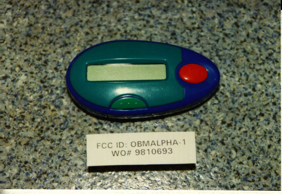
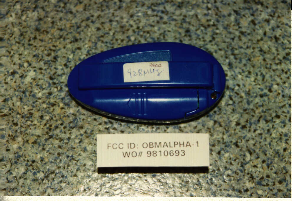
OBMALPHA-1Alpha-numeic pager
VTech Connect Limited
Click to zoom
Application Details
- Equipment Class
- CXX - Communications Rcvr for use w/ licensed Tx and CBs
- Date of Grant
- Mar 02, 1999
- Application Purpose
- Original Equipment
- Date of Application
- Jan 18, 1999
- Equipment Note
- Alpha-numeic pager
- Frequency Range
- 932.00000000 - 932.00000000
- Company
- VTech Connect Limited
- Country
- Hong Kong
Documents & Files
Document Text
Text extracted from the exhibit documents filed with the FCC. Open a document above to read the original.
Block Diagram
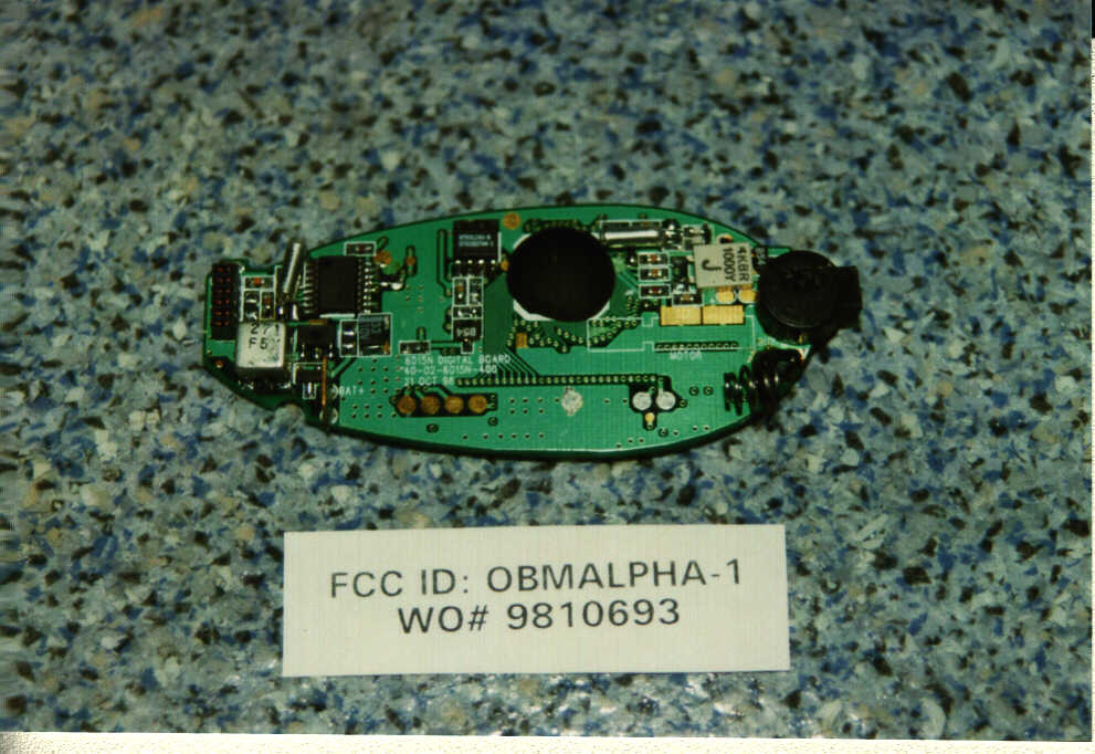
Cirkisys Electronics Limited All Rights Reserved KS57C21116 4 bits MCU (ROM 16 K) (RAM 3584 x 4) 2.7 V POCSAG decoder 93C46 EEPROM SEG0-SEG31 & COM0-COM7 LCD Bus I/O port Lamp buzzer motor 4 bit interrupt 2.1V Volt. detector Timer RF Board 1.5 V BatteryDC/DC convertor 76.8K Hz clock 32.768K Hz Clock 1M Hz Clock reset 16 character + icon key key Function Read I/O port & Interrupt & SPI FSK LVA BS1 BS2 Block diagram of 6015N digital board Cirkisys Electronics Limited All Rights Reserved cascode amp saw filter mixer crystal oscillator 21.4M Crystal filter FM-IF regulated 1V BS1 FSK data BS2 or QC battery LVA loop antenna Block diagram of 2-level FSK RF demodulation architecture
Operational Description
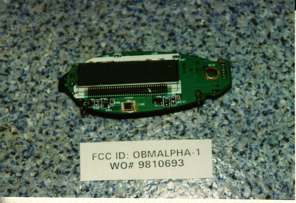
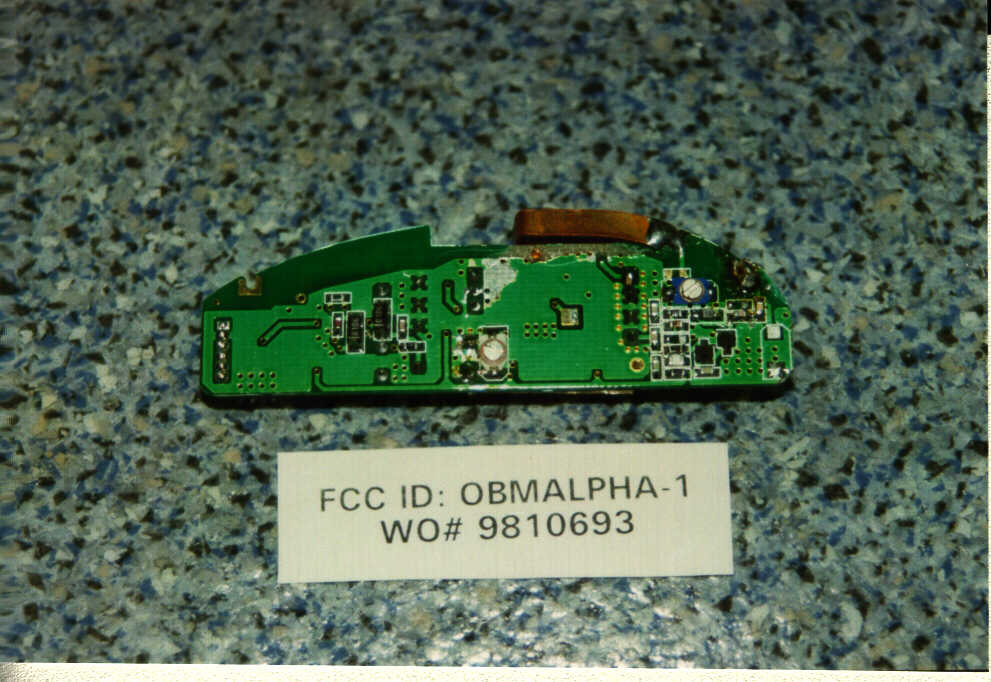
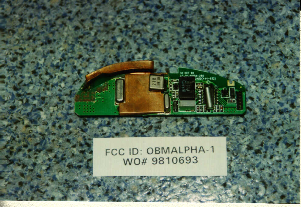
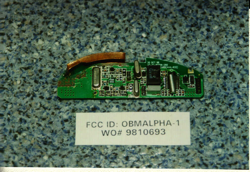
Cirkisys Electronics Limited All Rights Reserved Digital Board Hardware description A)Overview The Alpha One Pager is a POCSAG alpha-numeric pager. It has two key and 16 character (14- segment type) LCD display. It is controlled by Samsung KS57C21116 4-bit MCU. The POSCAG data is received by the decoder SM8212B and will store to the memory (RAM) of the MCU. The user can use the key to read the received message. The message will display the LCD glass and will scroll if more than 16 character. When the new user message is arrived, the pager can set the alert signal to user such as buzzing sound or vibration from vibrator. B)POCSAG decoder The POCSAG decoder SM8212M is used to connect the RF board to MCU of the digital board. The decoder will control the RF board ON & OFF and receive the FSK data. The decoder will decode the FSK signal and acknowledge the MCU if CAP code is correct. When the new message arrive, the decoder will generate the interrupt to the MCU. The decoder will also generate the low battery signal to the MCU if voltage is below 1.1V. The 76.8K Hz crystal is used to drive the POCSAG decoder. C)MCU The core MCU is Sumsung KS57C21116 which will handle all the work of pager. The MCU will has a initial procedure that will read setting from EEPROM and setup the I/O device. The MCU will receive the RF signal thu RF board and POCSAG decoder. After MCU receive the signal with respect address, it will turn the buzzer on or motor on to acknowledge the user. The user can access the pager by the key input to read the message from the LCD. The 1M Hz and 32.768K Hz crystal is used to drive the MCU. The DC/DC convertor step up the 1.5V to 2.7V from battery to supply the MCU, decoder and EEPROM. A 2.1V voltage detector is used as reset circuit to the MCU. D)I/O DEVICE LCD -The fully ON LCD display profile is shown on the block diagram. It contains 16 14-segment character and five icon on the top. It can check in the test mode. EEPROM - 93C46, 1K bit serial EEPROM, is used to save the configuration information. Buzzer & Motor -is used to acknowledge the user. Lamp -is used to see the LCD in darkness place. Cirkisys Electronics Limited All Rights Reserved Page 2 KS57C21116 4 bits MCU (ROM 16 K) (RAM 3584 x 4) 2.7 V POCSAG decoder 93C46 EEPROM SEG0-SEG31 & COM0-COM7 LCD Bus I/O port Lamp buzzer motor 4 bit interrupt 2.1V Volt. detector Timer RF Board 1.5 V BatteryDC/DC convertor 76.8K Hz clock 32.768K Hz Clock 1M Hz Clock reset 16 character + icon key key Function Read I/O port & Interrupt & SPI FSK LVA BS1 BS2 Block diagram of 6015N digital board Cirkisys Electronics Limited All Rights Reserved Technical Description and Block diagram of 6015 pager - RF part A)Theory of Operation The RF demodulation process is based on conventional double conversion superheterodyne method. The first IF (intermediate frequency) is selected to be 21.4MHz. The second IF is 455KHz. The demodulation process is done by the FM-IF IC (KA8514) or TA31145. The FM-IF IC includes voltage regulator, low battery detection circuit, mixer, oscillator, FSK comparator and limiting IF amplifier. The operation principles of this paging receiver are depicted in Fig. 1 and the schematics. B)Antenna Circuit and Amplifier Antenna of the pager is constructed by silver plated copper loop. By proper tuning a variable capacitor, the loop antenna will be matched to the amplifier and hence the signal picked up would be amplified. The amplified RF signal is then applied to a mixer through a wide-band SAW filter. The SAW filter is mainly used for first image signal suppression. C)First Local Oscillator and Mixer The oscillating signal is generated by a crystal oscillator with one stage of frequency multiplier. The LO signal is then mixed with the RF signal by mixer to generate the 21.4MHz IF signal. The 21.4MHz crystal filter is used to filter the 21.4MHz IF signal with second image rejection purpose. D)FM-IF Circuit The FM-IF IC converts the 21.4MHz IF signal to 455KHz second IF by the internal second mixer with externally connected crystal of either 20.945MHz. Ceramic filters are used to improve the adjacent channel rejection response. The 455KHz IF signal will then be amplified, limited and discriminated by a ceramic resonator to the base-band analogue signal. Inside the chip there is a level comparator for converting the analogue signal to the digital data. Besides, the chip can power up the whole RF front end with a regulated 1Vdc. With the low voltage alarm function, the MCU can detect the battery from running flat. cascode amp saw filter mixer crystal oscillator 21.4M Crystal filter FM-IF regulated 1V BS1 FSK data BS2 or QC battery LVA loop antenna Figure 1: Block diagram of 2-level FSK RF demodulation architecture. Cirkisys Electronics Limited All Rights Reserved E)Frequency of the first and second local oscillator Here attached the frequency of the first local oscillator, e.g. 1. for 928MHz pager sample, the frequency generated from the local oscillator is 75.550MHz and its harmonic. 2. for 932MHz pager sample, the frequency generated from the local oscillator is 75.883MHz and its harmonic. The second local oscillator is fixed at 20.945MHz.
Test Report
• The test results reported in this test report shall refer only to the sample actually tested and shall not refer or be deemed to refer to bulk from which such a sample may be said to have been obtained. • This report shall not be reproduced except in full without prior authorization from Intertek Testing Services Hong Kong Limited FCC ID: OBMALPHA-1 Cirkisys Electronics Limited Application For Certification (FCC ID: OBMALPHA-1) Superheterodyne Receiver WO# 9810693 CKL/at January 12, 1999 INTERTEK TESTING SERVICES FCC ID: OBMALPHA-1 i LIST OF EXHIBITS INTRODUCTION EXHIBIT 1:General Description EXHIBIT 2:System Test Configuration EXHIBIT 3:Emission Results EXHIBIT 4:Equipment Photographs EXHIBIT 5:Product Labelling EXHIBIT 6:Technical Specifications EXHIBIT 7:Instruction Manual EXHIBIT 8:Miscellaneous Information INTERTEK TESTING SERVICES FCC ID: OBMALPHA-1 ii MEASUREMENT/TECHNICAL REPORT Cirkisys Electronics Limited - MODEL: 6015N FCC ID: OBMALPHA-1 This report concerns (check one:)Original Grant X Class II Change Equipment Type: Superheterodyne Receiver (example: computer, printer, modem, etc.) Deferred grant requested per 47 CFR 0.457(d)(1)(ii)?Yes No X If yes, defer until: date Company Name agrees to notify the Commission by: date of the intended date of announcement of the product so that the grant can be issued on that date. Transition Rules Request per 15.37?Yes No X If no, assumed Part 15, Subpart B for unintentional radiator - the new 47 CFR [10-1-96 Edition] provision. Report prepared by:Wilbur Ng Intertek Testing Services Hong Kong Ltd. 2/F., Garment Centre, 576, Castle Peak Road, Kowloon, Hong Kong Phone:852-746-8680 Fax:852-785-5487 INTERTEK TESTING SERVICES FCC ID: OBMALPHA-1 iii Table of Contents 1.0 General Description................................................................................................................. 2 1.1 Product Description ................................................................................................................ 2 1.2 Related Submittal(s) Grants .................................................................................................... 2 1.3 Test Methodology ................................................................................................................... 3 1.4 Test Facility ............................................................................................................................ 3 2.0 System Test Configuration...................................................................................................... 5 2.1 Justification............................................................................................................................. 5 2.2 EUT Exercising Software ....................................................................................................... 5 2.3 Special Accessories ......................................................................................................................5 2.4 Equipment Modification ......................................................................................................... 6 2.5 Support Equipment List and Description ....................................................................................6 3.0 Emission Results....................................................................................................................... 8 3.1 Field Strength Calculation....................................................................................................... 9 3.2 Radiated Emission Configuration Photograph ...................................................................... 10 3.3 Radiated Emission Data ........................................................................................................ 11 4.0 Equipment Photographs........................................................................................................ 15 5.0 Product Labelling................................................................................................................... 17 6.0 Technical Specifications......................................................................................................... 19 7.0 Instruction Manual................................................................................................................ 21 8.0 Miscellaneous Information.................................................................................................... 23 8.2 Discussion of Pulse Desensitization...................................................................................... 24 8.3 Calculation of Average Factor ..............................................................................................25 8.4 Emissions Test Procedures.................................................................................................... 26 INTERTEK TESTING SERVICES FCC ID: OBMALPHA-1 iv List of attached file Exhibit typefilename Test Reportreport.doc Test Setup Photoradiated.jpg External Photoophoto1.jpg to ophoto2.jpg Internal Photoiphoto1.jpg to iphoto5.jpg Block Diagramblock.pdf Schematicscircuit.pdf ID Label/Locationlabel.pdf User Manualmanual.pdf Cover Letterletter.pdf Circuit Descriptiondescri.pdf INTERTEK TESTING SERVICES FCC ID: OBMALPHA-1 1 EXHIBIT 1 GENERAL DESCRIPTION INTERTEK TESTING SERVICES FCC ID: OBMALPHA-1 2 1.0General Description 1.1Product Description The Alpha One Pager is a POCSAG alpha-numeric pager. It can operate at frequency 928MHz or 932 MHz by choosing corresponding value of X1. Detailed information can refer to circuit diagram. It has two key and 16 character (14-segment type) LCD display. It is controlled by Samsung KS57C21116 4-bit MCU. The POSCAG data is received by the decoder SM8212B and will store to the memory (RAM) of the MCU. The user can use the key to read the received message. The message will display the LCD glass and will scroll if more than 16 character. When the new user message is arrived, the pager can set…
Text truncated - open the document above for the full version.
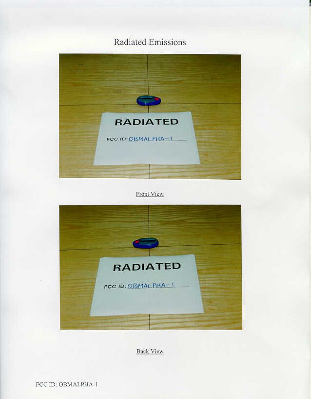
Test Setup Photos
• The test results reported in this test report shall refer only to the sample actually tested and shall not refer or be deemed to refer to bulk from which such a sample may be said to have been obtained. • This report shall not be reproduced except in full without prior authorization from Intertek Testing Services Hong Kong Limited FCC ID: OBMALPHA-1 Cirkisys Electronics Limited Application For Certification (FCC ID: OBMALPHA-1) Superheterodyne Receiver WO# 9810693 CKL/at January 12, 1999 INTERTEK TESTING SERVICES FCC ID: OBMALPHA-1 i LIST OF EXHIBITS INTRODUCTION EXHIBIT 1:General Description EXHIBIT 2:System Test Configuration EXHIBIT 3:Emission Results EXHIBIT 4:Equipment Photographs EXHIBIT 5:Product Labelling EXHIBIT 6:Technical Specifications EXHIBIT 7:Instruction Manual EXHIBIT 8:Miscellaneous Information INTERTEK TESTING SERVICES FCC ID: OBMALPHA-1 ii MEASUREMENT/TECHNICAL REPORT Cirkisys Electronics Limited - MODEL: 6015N FCC ID: OBMALPHA-1 This report concerns (check one:)Original Grant X Class II Change Equipment Type: Superheterodyne Receiver (example: computer, printer, modem, etc.) Deferred grant requested per 47 CFR 0.457(d)(1)(ii)?Yes No X If yes, defer until: date Company Name agrees to notify the Commission by: date of the intended date of announcement of the product so that the grant can be issued on that date. Transition Rules Request per 15.37?Yes No X If no, assumed Part 15, Subpart B for unintentional radiator - the new 47 CFR [10-1-96 Edition] provision. Report prepared by:Wilbur Ng Intertek Testing Services Hong Kong Ltd. 2/F., Garment Centre, 576, Castle Peak Road, Kowloon, Hong Kong Phone:852-746-8680 Fax:852-785-5487 INTERTEK TESTING SERVICES FCC ID: OBMALPHA-1 iii Table of Contents 1.0 General Description ................................................................................................................. 2 1.1 Product Description ................................................................................................................ 2 1.2 Related Submittal(s) Grants .................................................................................................... 2 1.3 Test Methodology ................................................................................................................... 3 1.4 Test Facility ............................................................................................................................ 3 2.0 System Test Configuration ...................................................................................................... 5 2.1 Justification............................................................................................................................. 5 2.2 EUT Exercising Software ....................................................................................................... 5 2.3 Special Accessories ......................................................................................................................5 2.4 Equipment Modification ......................................................................................................... 6 2.5 Support Equipment List and Description ....................................................................................6 3.0 Emission Results ....................................................................................................................... 8 3.1 Field Strength Calculation....................................................................................................... 9 3.2 Radiated Emission Configuration Photograph ...................................................................... 10 3.3 Radiated Emission Data ........................................................................................................ 11 4.0 Equipment Photographs ........................................................................................................ 15 5.0 Product Labelling ................................................................................................................... 17 6.0 Technical Specifications ......................................................................................................... 19 7.0 Instruction Manual ................................................................................................................ 21 8.0 Miscellaneous Information .................................................................................................... 23 8.2 Discussion of Pulse Desensitization...................................................................................... 24 8.3 Calculation of Average Factor ..............................................................................................25 8.4 Emissions Test Procedures.................................................................................................... 26 INTERTEK TESTING SERVICES FCC ID: OBMALPHA-1 iv List of attached file Exhibit typefilename Test Reportreport.doc Test Setup Photoradiated.jpg External Photoophoto1.jpg to ophoto2.jpg Internal Photoiphoto1.jpg to iphoto5.jpg Block Diagramblock.pdf Schematicscircuit.pdf ID Label/Locationlabel.pdf User Manualmanual.pdf Cover Letterletter.pdf Circuit Descriptiondescri.pdf INTERTEK TESTING SERVICES FCC ID: OBMALPHA-1 1 EXHIBIT 1 GENERAL DESCRIPTION INTERTEK TESTING SERVICES FCC ID: OBMALPHA-1 2 1.0 General Description 1.1Product Description The Alpha One Pager is a POCSAG alpha-numeric pager. It can operate at frequency 928MHz or 932 MHz by choosing corresponding value of X1. Detailed information can refer to circuit diagram. It has two key and 16 character (14-segment type) LCD display. It is controlled by Samsung KS57C21116 4-bit MCU. The POSCAG data is received by the decoder SM8212B and will store to the memory (RAM) of the MCU. The user can use the key to read the received message. The message will display the LCD glass and will scroll if more than 16 character. When the new user message is arrived, the page…
Text truncated - open the document above for the full version.
Contact Information
Applicant
Ricky K. W. Chan(Engineering Manager)
852-2409-2022Fax: 852-2612-0661
Technical Contact
INTERTEK TESTING SERVICES HONG KONG LTDWILBUR NG
[email protected](852) 2746-8211
2/F., GARMENT CENTRE, · KOWLOON · Hong Kong
Non-Technical Contact
INTERTEK TESTING SERVICES HONG KONG LTDWILBUR NG
[email protected](852) 2746-8211
Test Firm
Intertek Testing Services Hong KongBilly Chow
Technical Specifications
| # | Rule Parts | Frequency Range | Power Output |
|---|---|---|---|
| 2 | 15B | 932 MHz - 932 MHz | - |
Other Applications from VTech Connect Limited

OBM8003N-930
Mar 16, 2000Wireless Email Unit
Equipment Class
CXX - Communications Rcvr for use w/ licensed Tx and CBs
OBM8015-930
Mar 07, 2000Alphanumeric Flex Pager
Equipment Class
CXX - Communications Rcvr for use w/ licensed Tx and CBs
OBM6018-930
Feb 01, 2000Pager
Equipment Class
CXX - Communications Rcvr for use w/ licensed Tx and CBs
OBM8001-930
Nov 22, 1999Pager
Equipment Class
CXX - Communications Rcvr for use w/ licensed Tx and CBs
OBM8022-155
Oct 08, 1999CXX - Communications Rcvr for use w/ licensed Tx and CBs
Equipment Class
CXX - Communications Rcvr for use w/ licensed Tx and CBs