OC3BM1871Bluetooth module 4.0 single mode
NovaComm Technologies Inc.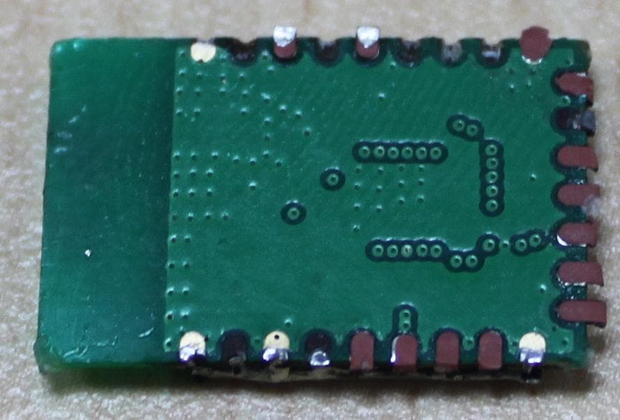
Click to zoom
Application Details
- Equipment Class
- DTS - Digital Transmission System
- Date of Grant
- Apr 21, 2013
- Application Purpose
- Original Equipment
- Date of Application
- Apr 01, 2013
- Equipment Note
- Bluetooth module 4.0 single mode
- Frequency Range
- 2402.00000000 - 2480.00000000
- Company
- NovaComm Technologies Inc.
- Country
- China
Documents & Files
Document Text
Text extracted from the exhibit documents filed with the FCC. Open a document above to read the original.
Users Manual
NovaComm Technologies Inc. Rev: 1.0 3/15/2013 NVC-MDCS71 Bluetooth Module OEM General User and Installation Guide I. OEM Usage Instructions Installation The NVC-MDCS71 is a surface mount Bluetooth module supplied are 22 and 13 pin, 4-layer PCB. The final assembly recommended reflow profiles are: For RoHS/Pb-free applications, Sn96.5/Ag3.0/Cu0.5 solder is recommended. Maximum peak temperature of 230° - 240°C (below 250°C). Maximum rise and fall slope after liquidous of < 2°C/second. Maximum rise and fall slope after liquidous of < 3°C/second. Maximum time at liquidous of 40 – 80 seconds. Layout The area around the NVC-MDCS71 module should be free of any ground planes, trace routings, or metal for at least 6mm from the antenna in all directions. Traces should not be routed underneath the module. Crystal Tuning and Power Calibration These steps are performed by the manufacturer, and must NOT be modified from the settings applied during manufacturing. Any changes to these settings may void the user’s authority to operate this equipment. Operating Conditions The permitted operating and storage temperatures, power supply requirements, and I/O tolerances are specified in the NVC-MDCS71 Datasheet. RF Exposure Warning This equipment complies with FCC radiation exposure limits set forth for an uncontrolled environment. This device's external antenna must be installed in accordance with provided instructions and it must be operated with a minimum of 20 cm spacing between antennas and all persons’ bodies (excluding extremities of hands, wrists and feet) during wireless mode of operation. Further, this transmitter must not be co-located or operated in conjunction with any other antenna or transmitter. II. Notice of FCC Regulatory Compliance This module has been tested and found to comply with the FCC Part15 Rules. These limits are designed to provide reasonable protection against harmful interference in approved installations. This equipment generates, uses, and can NovaComm Technologies Inc. Rev: 1.0 3/15/2013 radiate radio frequency energy and, if not installed and used in accordance the instructions, may cause harmful interference to radio communications. However, there is no guarantee that interference will not occur in a particular installation. This device complies with part 15 of the FCC Rules. Operation is subject to the following two conditions: (1) This device may not cause harmful interference, and (2) this device must accept any interference received, including interference that may cause undesired operation. Modifications or changes to this equipment not expressly approved by Amp’ed RF Technology Inc. may void the user’s authority to operate this equipment. III. Modular Approval FCC ID: OC3BM1871 In accordance with FCC Part 15, the NVC-MDCS71 is listed above as a Modular Transmitter device. In support of Modular Transmitter Approval, the following is stated: 1) The module does have buffered modulation / data inputs. 2) The module does regulate its own power supply. 3) The module does have a permanently attached antenna. 4) The module can be tested as a stand-alone device. 5) The module is labeled with the proper FCC ID, and labeling instructions are provided to OEM end users for external product labels. 6) The module does have instruction for proper use. 7) The module does meet the FCC RF regulations. IV. FCC Label Instructions The outside of final products that contain a NVC-MDCS71 device must display a label referring to the enclosed module. This exterior label can use wording such as the following: “Contains Transmitter Module FCC ID: OC3BM1871.” Any similar wording that expresses the same meaning may be used. An example of this label is figure 1 below: NovaComm Technologies Inc. Rev: 1.0 3/15/2013 Figure 1: External Device FCC Label Sample
Cover Letter(s)
NovaComm Technologies Inc. Part Number: NVC-MDCS71 FCC ID: OC3BM1871 Request for Modular Approval 15.3.2013 In accordance with FCC part 15, we, NovaComm technologies Inc, hereby request a modular level approval as outlined in FCC document DA001407, for the device listed above. In support of the Limited Modular Transmitter Approval, the following is stated: 1) The module does have buffered modulation / data inputs. 2) The module does regulate its own power supply. 3) The module does have a permanently attached antenna. 4) The module can be tested as a stand-alone device. 5) The module is labeled with the proper FCC ID, and labeling instructions are provided to OEM end users for external product labels. 6) The module does have instruction for proper use. 7) The module does meet the FCC RF regulations. Signature: Wang feng Director NovaComm technologies Inc. 902a,#560shengxia Rd.ZJ Innopark,shanghai,china
External Photos
Prüfbericht - Nr.: Test Report No.: 15059431 001 1. Photographs of EUT Photograph 1: Prüfbericht - Nr.: Test Report No.: 15059431 001 Backside
ID Label/Location Info
Label Location Explanation: As shown in the box behind the dotted yellow line is label location.
Internal Photos
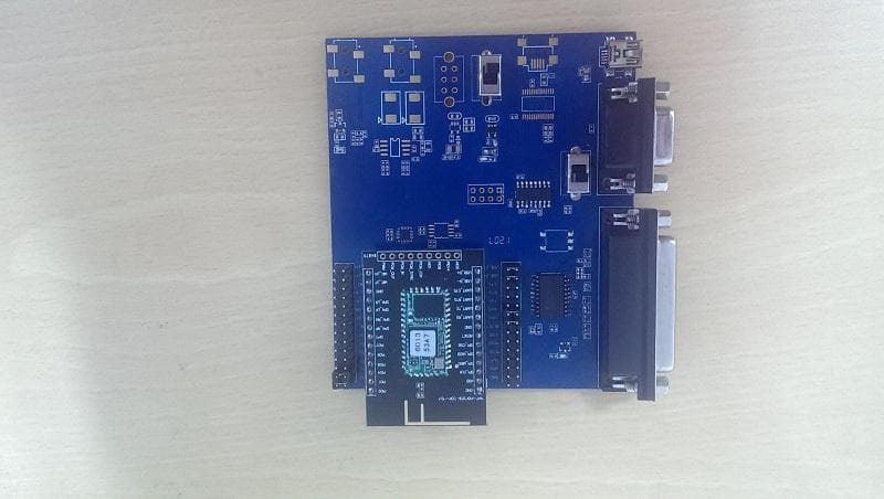
Prüfbericht - Nr.: Test Report No.: 15059431 001 1. Photographs of EUT Photograph 1: Prüfbericht - Nr.: Test Report No.: 15059431 001 Photograph 2: Without Shield cover Prüfbericht - Nr.: Test Report No.: 15059431 001 Host Photograph 3 : Host with the module installed
RF Exposure Info
Produkte Products RF Exposure Statement: Page 1 of 1 Client: NovaComm technologies Inc. 902a,#560shengxia Rd.ZJ Innopark,shanghai,china Test item: Bluetooth Module 4.0 single mode Identification: Mode name :NVC-MDCS71 FCC ID : OC3BM1871 FCC Requirement According to FCC 2.1091, mobile equipment must comply with the following applicable limit for maximum permissible exposure (MPE) specified in FCC 1.1310: Equipment Use Frequency Range Power Density [mW/cm 2 ] Average Time [min] General Population / Uncontrolled Exposure 1.5 – 100GHz 1 6 IC Requirement According to RSS-102 (Issue 4), clause 2.5.2, no routine RF exposure evaluation is required if the transmitter power (e.i.r.p.) is below the following threshold: Frequency Range SAR Limitation [W] Above 1.5GHz 5 Measurement Result The maximum measured transmitter power is the following: Conducted Output Power P out [mW] Maximum Antenna Gain [dBi] P out EIRP [mW] Power Density at 20cm [mW/cm 2 ] 3.3 2 5.23 0.00104 Note: The power density S in mW/cm 2 is calculated according to the Friis formula: S = (P S = power density in mW/cm 2 P out = antenna conducted output power in mW G = antenna gain in linear scale (here: 2dBi=10log(G)) D = distance between observation point and radiating structure in cm (here: 20cm) out · G) / (4π · D 2 ), where Conclusion The device complies with the FCC and IC RF exposure requirements since the maximum transmitter power density is below the FCC limit and the e.i.r.p. power is below the IC RF exposure evaluation exemption threshold. Refer to test repo rt 15059431 001 for more details. TÜV Rheinland (Shanghai) Co., Ltd. 10-15/F, Huatsing Building, No.88, Lane 777, Guangzhong Road West, Shanghai 200072, P.R. China
Test Report
TÜV Rheinland LGA Products Tillystrasse 2 D-90431 Nürnberg Tel.: +49 911 655 5225 Fax +49 911 655 5226 Mail: [email protected] Web: www.tuv.com QMA TRLP 6.1-350 Version: 1 01.08.2011 Produkte Products Prüfbericht - Nr.: 15059431 001 Test Report No.: Seite 1 von 37 Page 1 of 37 Auftraggeber: Client: NovaComm technologies Inc. 902a,#560shengxia Rd.ZJ Innopark,shanghai,china Gegenstand der Prüfung: Test item: Bluetooth Module 4.0 single mode Bezeichnung: Identification: NVC-MDCS71 FCC ID :OC3BM1871 Serien-Nr.: Serial No.: N/A Wareneingangs-Nr.: Receipt No.: 154014968 Eingangsdatum: Date of receipt: Zustand des Prüfgegenstandes bei Anlieferung: Condition of test item at delivery: Test sample(s) is/are not damaged and suitable for testing. Prüfort: Testing location: TÜV Rheinland (Shanghai) Co., Ltd. QuieTek Technology(Suzhou)Co., Ltd. (Detailed address refer to clause 2.1) Prüfgrundlage: Test specification: FCC 47 CFR Part 15, Subpart C, §15.247 ANSI C63.4-2009 ANSI C63.10-2009 KDB 558074 D01 DTS Meas Guidance v02 Prüfergebnis: Test Result: Der Prüfgegenstand entspricht oben genannter Prüfgrundlage(n). The test item passed the test specification(s). Prüflaboratorium: Testing Laboratory: TÜV Rheinland (Shanghai) Co., Ltd. Building 2, No. 777 Guangzhong Road West, Shanghai 200072, P.R. China geprüft/ tested by: 2013-03-19 Shili / Inspector kontrolliert/ reviewed by: 2013-03-19 Jesse Huang / Reviewer Datum Date Name/Stellung Name/Position Unterschrift Signature Datum Date Name/Stellung Name/Position Unterschrift Signature Sonstiges/ Other Aspects: Abkürzungen: P(ass) = entspricht Prüfgrundlage F(ail) = entspricht nicht Prüfgrundlage N/A = nicht anwendbar N/T = nicht getestet Abbreviations: P(ass) = passed F(ail) = failed N/A = not applicable N/T = not tested Dieser Prüfbericht bezieht sich nur auf das o.g. Prüfmuster und darf ohne Genehmigung der Prüfstelle nicht auszugsweise vervielfältigt werden. Dieser Bericht berechtigt nicht zur Verwendung eines Prüfzeichens. This test report relates to the a. m. test item. Without permission of the test center this test report is not permitted to be duplicated in extracts. This test report does not entitle to carry any safety mark on this or similar products. Produkte Products Prüfbericht - Nr.: Test Report No.: 15059431 001 Seite 2 von 37 Page 2 of 37 TEST SUMMARY 3.2.1 VOLTAGE REQUIREMENTS, FCC 15.31(E) RESULT: PASS 3.2.2 ANTENNA REQUIREMENTS, FCC 15.203, FCC 15.204 AND RSS-GEN 7.1.4 RESULT: PASS 5.1.1 CONDUCTED OUTPUT POWER, FCC 15.247(B)(3) AND RSS-210 A8.4(2) RESULT: PASS 5.1.2 6DB&99% BANDWIDTH, FCC 15.247(A)(2) AND RSS-210 A8.2(A) 5.1.3 POWER SPECTRAL DENSITY (PSD), FCC 15.247(E) AND RSS-210 A8.2 RESULT: PASS 5.1.4 CONDUCTED SPURIOUS EMISSION, FCC 15.247(D) AND RSS-210 A8.5 RESULT: PASS 5.1.5 BAND EDGE COMPLIANCE OF RF CONDUCTED EMISSION, FCC 15.247(D) AND RSS-210 A8.5 RESULT: PASS 6.1.1 BAND EDGE RADIATED EMISSION, FCC 15.205, FCC 15.209, FCC 15.247(D), RSS-210 2.2, RSS-210 2.6 AND RSS-210 A8.5 RESULT: Pass 6.1.2 RADIATED SPURIOUS EMISSION OF TRANSMITTER, FCC 15.205, FCC 15.209, FCC 15.247(D), RSS-210 2.2, RSS-210 2.6 AND RSS-210 A8.5 RESULT: PASS Produkte Products Prüfbericht - Nr.: Test Report No.: 15059431 001 Seite 3 von 37 Page 3 of 37 CONTENTS 1. GENERAL REMARKS ............................................................................................... 5 1.1 COMPLEMENTARY MATERIALS ................................................................................. 5 2. TEST SITES ............................................................................................................ 5 2.1 TEST FACILITIES ..................................................................................................... 5 2.2 LIST OF TEST AND MEASUREMENT INSTRUMENTS ...................................................... 6 2.3 MEASUREMENT UNCERTAINTY ................................................................................. 6 3. GENERAL PRODUCT INFORMATION ........................................................................... 7 3.1 PRODUCT FUNCTION AND INTENDED USE .................................................................. 7 3.2 SYSTEM DETAILS .................................................................................................... 7 3.2.1 Voltage Requirements, FCC 15.31(e).......................................................................................... 7 3.2.2 Antenna Requirements, FCC 15.203, FCC 15.204 and RSS-Gen 7.1.4 ..................................... 7 3.3 INDEPENDENT OPERATION MODES ........................................................................... 8 3.4 NOISE SUPPRESSING PARTS .................................................................................... 8 4. TEST SET-UP AND OPERATION MODES ..................................................................... 9 4.1 TEST METHODOLOGY .............................................................................................. 9 4.2 PHYSICAL CONFIGURATION FOR TESTING ................................................................. 9 4.3 TEST OPERATION AND TEST SOFTWARE ................................................................... 9 4.4 SPECIAL ACCESSORIES AND AUXILIARY EQUIPMENT ................................................. 9 4.5 COUNTERMEASURES TO ACHIEVE EMC COMPLIANCE ................................................ 9 5. TEST RESULTS OF CONDUCTED MEASUREMENTS AT ANTENNA PORT ....................... 10 5.1 TRANSMITTER PARAMETERS .................................................................................. 10 5.1.1 Conducted Output Power, FCC 15.247(b)(3) and RSS-210 A8.4(2) ......................................... 10 5.1.2 6dB&99% Bandwidth, FCC 15.247(a)(2) and RSS-210 A8.2(a) ............................................... 12 5.1.3 Power Spectral Density (PSD), FCC 15.247(e) and RSS-210 A8.2 .......................................... 16 5.1.4 Conducted Spurious Emission, FCC 15.247(d) and RSS-210 A8.5 .…
Text truncated - open the document above for the full version.
Test Setup Photos
Prüfbericht - Nr.: Test Report No.: 15059431 001 1. hotographs of the Test Setup Photograph 1: Set-up for Radiated Emission, 30MHz-1000MHz Prüfbericht - Nr.: Test Report No.: 15059431 001 Photograph 2: Set-up for Radiated Emission, 1G-18GHz Photograph 3: Set-up for Conduct Power
Contact Information
Applicant
Feng Wang(Director)
Technical Contact
NovaComm technologies Inc.Thomas Wang
[email protected]86 21 60453799
902a, #560shengxia Rd., ZJ Innopark, · Shanghai · China
Non-Technical Contact
NovaComm technologies Inc.Thomas Wang
[email protected]86 21 60453799
Test Firm
DEKRA Testing and Certification (Suzhou) Co., Ltd.Jerry Pan
Technical Specifications
| # | Rule Parts | Frequency Range | Power Output |
|---|---|---|---|
| 1 | 15C | 2.40 GHz - 2.48 GHz | 5.23 mW |
Other Applications from NovaComm Technologies Inc.
OC3BM1856
Jul 28, 2013Bluetooth Module
Equipment Class
DSS - Part 15 Spread Spectrum TransmitterOC3BM1842
Jul 30, 2012Bluetooth module
Equipment Class
DSS - Part 15 Spread Spectrum Transmitter
OC3BM1845
Jul 01, 2012Spread Spectrum Transmitter
Equipment Class
DSS - Part 15 Spread Spectrum Transmitter