OOJOPENCELLV1-1
OpenCell Corp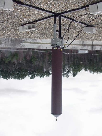
Click to zoom
Application Details
- Equipment Class
- TNB - Licensed Non-Broadcast Station Transmitter
- Date of Grant
- Aug 06, 2002
- Application Purpose
- Original Equipment
- Date of Application
- May 09, 2002
- Frequency Range
- 855.01250000 - 865.98750000
- Company
- OpenCell Corp
- Country
- United States
Documents & Files
Document Text
Text extracted from the exhibit documents filed with the FCC. Open a document above to read the original.
Users Manual
TRANSCEPT PROPRIETARY TRANSCEPT PROPRIETARY OPENCELL OPERATIONS AND MAINTENANCE MANUAL Document No. XXXXXXX Revision (DRAFT 2) April 10, 2002 T HIS DOCUMENT CONTAINS PROPRIETARY INFORMATION OF T RANSCEPT , I NC . AND IS NOT TO BE USED FOR ANY PURPOSE , EXCEPT IN ACCORDANCE WITH CONTRACTUAL NONDISCLOSURE TERMS . T HIS DOCUMENT IS NOT TO BE DUPLICATED IN WHOLE OR IN PART WITHOUT PRIOR WRITTEN PERMISSION FROM A DULY AUTHORIZED REPRESENTATIVE OF T RANSCEPT . OpenCellOperations and Maintenance ManualDoc. No. XXXXXXX - Page i T RANSCEPT P ROPRIETARY - DATA ON THIS PAGE SUBJECT TO RESTRICTIONS CITED ON COVER AND TITLE TABLE OF CONTENTS SectionPage 1.0INTRODUCTION.................................................................................................................. 1 1.1AB OUT THIS M ANU AL ............................................................................................................. 1 1.1.1Scope ............................................................................................................................ 1 1.1.2Manual Organization ..................................................................................................... 1 1.2T ERMINOLOGY , A CRONYMS AND ABBREVIATIONS .................................................................... 1 1.2.1Notations Conventions .................................................................................................. 1 1.2.2Acronyms and Abbreviations ........................................................................................ 1 1.3R EFERENCE D OCUMENTATION ............................................................................................... 2 1.4S YSTEM O VERVIEW ................................................................................................................ 2 1.4.1System Configuration.................................................................................................... 2 1.4.2General Description ...................................................................................................... 3 1.4.3Hub Subsystem Assemblies ......................................................................................... 4 1.4.3.1Base Station Interface Module (BIM) .................................................................... 5 1.4.3.2BIR Power Supply.................................................................................................. 5 1.4.3.3Central Processing Unit (CPU).............................................................................. 5 1.4.3.4System Interface (STF) ......................................................................................... 6 1.4.3.5Synchro nous Interface (SIF).................................................................................. 6 1.4.3.6Hub Down Converter (HDC).................................................................................. 6 1.4.3.7Forward Simulcast Card (FSC) ............................................................................. 6 1.4.3.8Reverse Simulcast Card (RSC)............................................................................. 6 1.4.3.9Hub Up Converter (HUC)...................................................................................... 6 1.4.3.10Hub Reference Module (HRM).............................................................................. 6 1.4.3.11Ethernet Hub.......................................................................................................... 6 1.4.3.12RF I/O Module (RFIO) ........................................................................................... 6 1.4.3.13Digital I/O Module (DIO) ........................................................................................ 7 1.4.3.14RF CompactPCI Chassis & Backplane ................................................................. 7 1.4.3.15Digital CompactPCI Chassis & Backplane............................................................ 7 1.4.3.16FIR CompactPCI Power Supply ............................................................................ 7 1.4.3.17Power Supply Interface (PSI) ................................................................................ 7 1.4.3.18Ethernet Hub Power Inverter (EHPI)..................................................................... 7 1.4.4RAN Subsystem Assemblies........................................................................................ 7 1.4.4.1Central Processing Unit (CPU).............................................................................. 7 1.4.4.2System Interface (STF) ......................................................................................... 7 1.4.4.3Synchro nous Interface (SIF).................................................................................. 7 1.4.4.4RAN Down Converter (RDC)................................................................................. 8 1.4.4.5RAN Up Converter (RUC)..................................................................................... 8 1.4.4.6RAN Chassis & Backplane .................................................................................... 8 1.4.4.7CompactPCI Power Supply (RPS)........................................................................ 8 1.4.4.8RAN Rectifier (RCT).............................................................................................. 8 1.4.4.9Power Amplifier (PA) ............................................................................................. 8 1.4.4.10PA Interface Co ntroller (PIC)................................................................................. 8 1.4.4.11Multiplexers ............................................................................................................8 1.4.4.12PA Fans .................................................................................................................8 1.4.4.13Fuses ...................................................................................................…
Text truncated - open the document above for the full version.
Cover Letter(s)
5/8/02 FCC ID: OOJOPENCELLV1-1 FCC ID: OOJOPENCELLV1-1 EXHIBIT 1 REQUEST FOR CONFIDENTIALITY
External Photos
5/11/02 FCC ID: OOJOPENCELLV1-1 FCC ID: OOJOPENCELLV1-1 6-1 EXHIBIT 6 PHOTOGRAPHS External Views Figure 6-1 RAN Front View 5/11/02 FCC ID: OOJOPENCELLV1-1 FCC ID: OOJOPENCELLV1-1 6-2 Figure 6-2 RAN Rear View 5/11/02 FCC ID: OOJOPENCELLV1-1 FCC ID: OOJOPENCELLV1-1 6-3 Figure 6-3 Detail of RF Connector Identification on Rear of RAN 5/11/02 FCC ID: OOJOPENCELLV1-1 FCC ID: OOJOPENCELLV1-1 6-4 Figure 6-4 RAN Side View 5/11/02 FCC ID: OOJOPENCELLV1-1 FCC ID: OOJOPENCELLV1-1 6-5 Figure 6-5 RAN Antenna 5/11/02 FCC ID: OOJOPENCELLV1-1 FCC ID: OOJOPENCELLV1-1 6-6 Figure 6-6 RAN Antenna Mounted on Pole 5/11/02 FCC ID: OOJOPENCELLV1-1 FCC ID: OOJOPENCELLV1-1 6-7 Figure 6-7 RAN Enclosure Mounted on Pole
ID Label/Location Info
5/11/02 FCC ID: OOJOPENCELLV1-1 FCC ID: OOJOPENCELLV1-1 EXHIBIT 2 PRODUCT LABELING Figure 2-1 Proposed RAN Label 5/11/02 FCC ID: OOJOPENCELLV1-1 FCC ID: OOJOPENCELLV1-1 Figure 2-2 Photo of Rear of RAN Showing Location of Proposed Label
Internal Photos
5/11/02 FCC ID: OOJOPENCELLV1-1 FCC ID: OOJOPENCELLV1-1 6-1 EXHIBIT 6 PHOTOGRAPHS Internal Views Figure 6-1 RAN, door open CPCI Chassis AC/DC Rectifiers Multiplexers Power Amp Compartment 5/11/02 FCC ID: OOJOPENCELLV1-1 FCC ID: OOJOPENCELLV1-1 6-2 Figure 6-2 RAN Compact PCI chassis 5/11/02 FCC ID: OOJOPENCELLV1-1 FCC ID: OOJOPENCELLV1-1 6-3 PCS Quadplexers 800 MHz Diplexer 800 MHz Triplexer PCS Primary PCS Diversity 5/11/02 FCC ID: OOJOPENCELLV1-1 FCC ID: OOJOPENCELLV1-1 6-4 Figure 6-3 Multiplexers installed in RAN Figure 6-4 Quadplexer, PCS Primary (Transmitting Blocks A/B/F) 5/11/02 FCC ID: OOJOPENCELLV1-1 FCC ID: OOJOPENCELLV1-1 6-5 Figure 6-5 Quadplexer, PCS Diversity (Transmitting Blocks C/D/E) 5/11/02 FCC ID: OOJOPENCELLV1-1 FCC ID: OOJOPENCELLV1-1 6-6 Figure 6-6 Cellular/SMR Triplexer 5/11/02 FCC ID: OOJOPENCELLV1-1 FCC ID: OOJOPENCELLV1-1 6-7 Figure 6-7 Cellular/SMR Duplexer 5/11/02 FCC ID: OOJOPENCELLV1-1 FCC ID: OOJOPENCELLV1-1 6-8 Figure 6-8 Power Amplifiers installed in RAN Figure 6-9 Power Amplifier 5/11/02 FCC ID: OOJOPENCELLV1-1 FCC ID: OOJOPENCELLV1-1 6-9 Figure 6-10 RUC Module, Top View 5/11/02 FCC ID: OOJOPENCELLV1-1 FCC ID: OOJOPENCELLV1-1 6-10 Figure 6-11 RUC circuit card (shield removed) 5/11/02 FCC ID: OOJOPENCELLV1-1 FCC ID: OOJOPENCELLV1-1 6-11 Figure 6-12 RUC Module, Bottom View
Operational Description
5/8/02 FCC ID: OOJOPENCELLV1-1 F C C ID: OOJOPENCELLV1-1 3-1 EXHIBIT 3 OPENCELL SYSTEM DESCRIPTION 3.1 Overview OpenCell is a cost-effective and flexible RF distribution system that is designed to simultaneously deploy the wireless services of several different carriers within a single unit. The OpenCell system consists of a centrally located Hub station and multiple Radio Access Nodes (RANs). The RANs are distributed throughout the target area to provide the desired coverage to mobile subscribers. RANs are installed at a roughly one-mile separation and are typically mounted on utility poles. RAN antennas are deployed on top of the pole at heights of 40-50 feet. The antenna radiates lower power than conventional sites (less than 10 watts), thus creating a microcellular footprint. Each RAN covers about a 0.5-mile range. Fiber optic cable interconnects each RAN to a centrally located OpenCell Hub. The Hub provides connectivity to the base transceiver station (BTS) of each wireless service provider that offers network service. The Hub converts the BTS RF signals to fiber optic backhaul. Each BTS can thus be interfaced to RAN sites up to 10 miles away. In a typical deployment, a tower company would complement its existing tower coverage "footprint" in a given area with a network of OpenCell systems. The tower company would normally own the OpenCell network equipment, and would lease access to its wireless service provider (WSP) tenants under long-term arrangements, similar to today’s conventional tower lease business. OpenCell operates across multiple frequencies and protocols, capable of the full range of digital services offered by WSPs. Each OpenCell RAN site can support up to 8 tenants simultaneously without interference or performance degradation. The OpenCell system is intended for service providers or tower aggregators. It is not intended for sale to the general public. 5/8/02 FCC ID: OOJOPENCELLV1-1 F C C ID: OOJOPENCELLV1-1 3-2 Figure 3-1 OpenCell Architecture FIBER RAN #N . . . Hub BTS Se ctor 1 Primary Diversity RF RF GPS RAN #1 GPS Mobile Subscribers Tx Figure 3-2 OpenCell Top Level Diagram 5/8/02 FCC ID: OOJOPENCELLV1-1 F C C ID: OOJOPENCELLV1-1 3-3 3.2 Frequency Plan and Output Power Each RAN equipment set can accommodate up to 8 tenants. Each tenant provides a specific service (cellular, PCS, or SMR) and a protocol associated with that service (i.e. GSM, TDMA, CDMA, etc). One tenant may reside within each available PCS, cellular, or SMR block. The minimum number of carriers per tenant is 1. The maximum number of carriers per tenant varies from 6 to 8, depending upon the selected protocol. Output power per tenant is approximately 4 watts nominal (the combined total of all carriers within a particular tenant’s block). The maximum output power may vary slightly, depending upon the selected protocol. Refer to Table 3-1 below. Where a tenant is employing multiple carriers, output power per tenant is divided equally among each carrier. Service/ Protocol Base Station Transmit Frequency Range, MHz Maximum # Tenants per Service per RAN location Maximum # Carriers per tenant Nominal Power per tenant (composite at RAN output, dBm) PCS CDMA635.2 1xRTT636.4 GSM836.4 TDMA835.7 Cellular TDMA834.7 GSM 869-894 835.4 CDMA634.2 1xRTT634.2 SMR iDEN855-866 3 ( for the combined SMR/ cellular services) 834.7 Table 3-1 OpenCell Frequency/Power Capability The valid range of channel center frequencies and carrier spacing within a band/block is dependent upon the selected protocol. The channel center frequency is selectable by the operator. The valid range of transmit center frequencies is set up such that all selectable channels, including those at the block edges, will not cause spurious or out- of-band requirements to be exceeded at maximum rated power levels. Center frequency spacing is controlled by the WSP BTS. The OpenCell system will support a minimum spacing shown for each protocol in Tables 3-2, 3-3 and 3-4. 5/8/02 FCC ID: OOJOPENCELLV1-1 F C C ID: OOJOPENCELLV1-1 3-4 Output power is primarily dictated by the BTS input level and preset gain settings. In addition, Forward Gain Control (FGC) within the OpenCell system will maintain a constant gain throughout the OpenCell forward path to within +/- 2 dB over all conditions. PCS Block Designator ABCDE F 1930-1945 1950-1965 1975-1990 1945-1950 1965-1970 1970-1975 ProtocolMin Carrier Spacing Valid Center Frequency Ranges (MHz) CDM A 1.25 MHz1931.250 to 1943.750 1951.250 to 1963.750 1976.250 to 1988.750 1946.250 to 1948.750 1966.250 to 1968.750 1971.250 to 1973.750 1xRTT 1.25 MHz1931.250 to 1943.750 1951.250 to 1963.750 1976.250 to 1988.750 1946.250 to 1948.750 1966.250 to 1968.750 1971.250 to 1973.750 GSM 800 kHz1930.200 to 1944.800 1950.200 to 1964.800 1975.200 to 1989.800 1945.200 to 1949.800 1965.200 to 1969.800 1970.200 to 1974.800 TDMA 360 kHz1930.020 to 1944.980 1950.020 to 1964.980 1975.020 to 1989.980 1945.020 to 1949.980 1965.020 to 1969.980 1970.020 to 1974.980 Table 3-2 PCS Tuning Ranges Cellular Block Designator AB 869-880 (A'', A) 890-891.5 (A') 880-890 (B) 891.5-894 (B') ProtocolMin Carrier Spacing Valid Center Frequency Ranges(MHz) TDMA 360 kHz869.020 to 879.980 890.020 to 891.480 880.020 to 889.980 891.520 to 893.980 GSM 800 kHz869.200 to 879.800 890.200 to 891.300 880.200 to 889.800 891.700 to 893.800 CDM A 1.25 MHz869.750 to 879.250 890.750 880.750 to 889.250 892.250 to 893.250 1xRTT 1.25 MHz869.750 to 879.250 890.750 880.750 to 889.250 892.250 to 893.250 Table 3-3 Cellular Tuning Ranges 5/8/02 FCC ID: OOJOPENCELLV1-1 F C C ID: OOJOPENCELLV1-1 3-5 ProtocolMin Carrier Spacing Valid Center Frequency Range (MHz) iDEN 350 kHz855.0125 to 865.9875 Table 3-4 SMR Tuning Range 3.3 System Interconnections OpenCell system interconnections include: • AC Power to RAN (240 VAC, 10 amps each, nominal) • 48VDC power to Hub • RF connections from RAN to antenna (PCS, cellular/SMR, and GPS) • Ethernet (from Hub to remotely located operator station) •…
Text truncated - open the document above for the full version.
Parts List/Tune Up Info
5/8/02 FCC ID: OOJOPENCELLV1-1 FCC ID: OOJOPENCELLV1-1 Tune-Up Information No special hardware adjustments are required to set or adjust the transmit frequency. The operating frequency is set by the operating software’s channel selection capability.
RF Exposure Info
5/8/02 FCC ID: OOJOPENCELLV1-1 FCC ID: OOJOPENCELLV1-1 EXHIBIT 8 RF EXPOSURE INFORMATION The OpenCell system is categorically excluded from routine environmental evaluation for radiofrequency hazards per 47 CFR 1.1307. When operated and installed in accordance with the instructions, the OpenCell system complies with regulations for radiofrequency radiation exposure limits in accordance with 47CFR 1.1310.
Test Report
Part 15 Laboratory Measurements and ANSI C63.4-1992 Project 3021924 Revision: April 26, 2000 Page 1 of 21 This document may not be reproduced except in its entirety without written permission from ITS. Emissions Testing Performed on the Transcept, Inc. Opencell RAN (Base and Expansion Unit) Part Number: 1000801G001 To FCC Part 15, Subpart B, Class A Date of Test: April 16, 2002 Project 3021924 Contact: Mr. Mike Prussel All services undertaken are subject to the following general policy: Reports are submitted for exclusive use of the client to whom they are addressed. Their significance is subject to the adequacy and representative character of the samples and to the comprehensiveness of the tests, examinations or surveys made. No quotations from reports or use of Intertek Testing Services NA Inc. name is permitted except as expressly authorized by Intertek Testing Services NA Inc. in writing. This report must not be used to claim product endorsement by NVLAP, NIST or any other agency of the U.S. Government. INTERTEK TESTING SERVICES NA, INC. Part 15 Laboratory Measurements and ANSI C63.4-1992 Project 3021924 Revision: April 26, 2000 Page 2 of 21 This document may not be reproduced except in its entirety without written permission from ITS. Table of Contents 1.0 Introduction and Conclusions........................................................................................3 2.0 Description of the Product.............................................................................................4 2.1 Brief Description and Received Condition...................................................................4 2.2 System Block Diagram....................................................................................................4 2.3 System Test Configuration.............................................................................................5 2.4 Justification.....................................................................................................................7 2.5 Description of how EUT was exercised during test.....................................................7 2.6 Modifications Required for Compliance......................................................................7 3.0 Radiated Emission..........................................................................................................8 3.1 Radiated Emissions Limits.............................................................................................8 3.2 Field Strength Calculation.............................................................................................9 3.3 Configuration Photographs - Worst-Case Radiated Emission.................................10 3.4 Test Data........................................................................................................................11 4.0 AC Mains Line-Conducted Emissions........................................................................12 4.1 Line-Conducted Emission Limits................................................................................12 4.2 Configuration Photographs - Worst-Case Line-Conducted Emission.....................13 4.3 Test Data........................................................................................................................14 5.0 Miscellaneous Information...........................................................................................16 5.1 Site Description.............................................................................................................16 5.2 Test Procedure Reference............................................................................................17 5.3 Labeling - USA..............................................................................................................18 5.4 Labelling - Canada........................................................................................................19 5.5 Test Report Certification.............................................................................................20 5.6 Equipment List..............................................................................................................21 INTERTEK TESTING SERVICES NA, INC. Part 15 Laboratory Measurements and ANSI C63.4-1992 Project 3021924 Revision: April 26, 2000 Page 3 of 21 This document may not be reproduced except in its entirety without written permission from ITS. This report is designed to show compliance with the FCC Part 15, Subpart B Rules for an unintentional radiator. The test procedures, as described in American National Standards Institute C63.4-1992, were employed. A description of the product and operating configuration, the various provisions of the rules, the methods for determining compliance, and a detailed summary of the results are included within this test report. 1.0 Introduction and Conclusions On April 16, 2002, we tested the Opencell RAN (Base and Expansion Unit), Part Number: 1000801G001, to determine if it was in compliance with the FCC Part 15, Subpart 15, Class B emissions limits. We found that the unit met the FCC Part 15 Subpart 15, Class B requirements when tested as received. This report is designed to show compliance with the following standards: FCC Part 15, Subpart B Rules for an Unintentional Radiator The test procedures described in American National Standards Institute C63.4: 1992, A description of the product and operating configurations, the various provisions of the rules, the methods for determining compliance and a detailed summary of the results are included within this test report. Configuration: In summary, this report verifies that the Opencell RAN (Base and Expansion Unit), Part Number: 1000801G001, is compliant with the FCC Part 15 Subpart 15, Class B requirements when production units conform to the initial sample. Please address all questions and comments concerning this report to Scott Lambert, Engineering Team Leader. INTERTEK TESTING SERVICES N…
Text truncated - open the document above for the full version.
Test Report
5/10/02 FCC ID: OOJOPENCELLV1-1 FCC ID: OOJOPENCELLV1-1 7-1 EXHIBIT 7 TEST RESULTS 7.1 Attestation 5/10/02 FCC ID: OOJOPENCELLV1-1 FCC ID: OOJOPENCELLV1-1 7-2 7.2 Test Instrumentation DescriptionModelManufacturer Spectrum Analyzer8593EHewlett Packard Power MeterE4418BHewlett Packard Power Sensor8481HHewlett Packard Vector Signal Generator CS2010Celerity Attenuator46-30-34Weinschel Attenuator ATT-0219-10- NNN-02 Midwest Microwave Attenuator ATT-0333-20- SMA-02 Midwest Microwave Coupler2202B-30Narda CouplerCK-48NMicrolab/FXR Digital Multimeter75Fluke Temperature ChamberT20C-3Tenney Table 7-1 Test Instrumentation 7.3 Description of Input Signals and Modulation Types The Celerity signal generator was used to accurately simulate RF input waveforms from the provider’s Base Transceiver Station (BTS). Signals were injected into the Hub at power levels within normal operating ranges. Each modulation type was tested separately. Peak/Average Ratio dB ProtocolMod TypeChannel Bit Rate Single carrierMax carriers TDMA π /4 DQPSK48.6 kbps3.29.7 CDMAQPSK1.228 Mcps (chip rate)11.511.5 CDMA2000QPSK1.228 Mcps (chip rate)11.511.5 GSMGMSK270.8 kbps0.26.1 iDEN16QAM64 kbps9.110.3 Table 7-2 Input Signal Description 5/10/02 FCC ID: OOJOPENCELLV1-1 FCC ID: OOJOPENCELLV1-1 7-3 7.4 General Test Setups Spectrum Analyzer Atten Directional Coupler Attenuator RAN Power Meter RF out Figure 7-1 Test setup for power output, occupied bandwidth, and emission mask Atten RAN Spectrum Analyzer RF out Figure 7-2 Test setup for conducted spurious emissions Test Antenna and Mast Ground Plane Hub Chassis RF in -48 VDC Power Signal Generator Ethernet RAN #1 RF Loads Computer AC Power (240 VAC, 60 Hz) Fiber Optic Battery Box RAN #2 Turntable EMI Measurement System Fiber Optic Figure 7-3 Test setup for radiated spurious emissions (also see separate report) 7.5 Power Output 7.5.1 Test Procedure The RAN transmitter output was connected to the power meter and spectrum analyzer using a directional coupler and RF attenuators as shown in Figure 7-1. The Celerity vector signal generator was used to inject actual system input signal levels and modulation types into the Hub. 5/10/02 FCC ID: OOJOPENCELLV1-1 FCC ID: OOJOPENCELLV1-1 7-4 Average power was measured using the power meter. Peak power was measured by setting the analyzer to peak detector, max hold, with resolution bandwidth and video bandwidth set to 3 MHz. Peak power measurements were performed on a single carrier basis for each protocol within the PCS band. 7.5.2 Results Maximum rated power at any RAN RF output port is as shown in the table below. Less power may be present, depending on the number of tenants served and the specific protocols used. RAN RF output port designation Measured power level, dBm Equivalent Power, watts Reference Figure PCS-P41.413.8Figure 7-49 PCS-D41.413.8Figure 7-51 Cell/SMR-D38.77.4Figure 7-52 Cell/SMR-P35.93.9Figure 7-32 Table 7-3 Measured Maximum Power per RF Port Maximum power per tenant is as shown below. Each tenant resides within one specific PCS, cellular or SMR block. Slightly less power is transmitted for other protocols. ServiceMaximum power level per tenant, dBm Equivalent Power, watts Reference Figures PCS36.94.9Figure 7-15 Figure 7-21 Cellular35.93.9Figure 7-31 Figure 7-32 SMR35.83.8Figure 7-45 Figure 7-48 Table 7-4 Measured Maximum Power per Tenant (per Block) 5/10/02 FCC ID: OOJOPENCELLV1-1 FCC ID: OOJOPENCELLV1-1 7-5 The table below summarizes the measured power output data. Measured power level, dBm ProtocolService# carriers AvgPeak Reference Figures CDMAPCS135.746.7Figure 7-5 CDMAPCS335.9Figure 7-6 CDMAPCS635.9Figure 7-7 CDMA2000PCS135.745.5Figure 7-9 CDMA2000PCS335.8Figure 7-10 CDMA2000PCS636.0Figure 7-11 GSMPCS136.637.0Figure 7-13 GSMPCS236.8Figure 7-14 Figure 7-15 GSMPCS436.6Figure 7-16 GSMPCS836.7Figure 7-17 TDMAPCS136.739.9Figure 7-19 TDMAPCS236.9Figure 7-20 Figure 7-21 TDMAPCS636.6Figure 7-22 Figure 7-23 TDMAPCS836.7Figure 7-24 CDMACell134.6Figure 7-26 CDMACell334.6Figure 7-27 CDMACell634.5Figure 7-28 GSMCell135.8Figure 7-30 GSMCell235.9Figure 7-31 GSMCell435.9Figure 7-32 GSMCell835.7Figure 7-33 TDMACell135.7Figure 7-35 TDMACell235.5Figure 7-37 TDMACell635.4Figure 7-39 TDMACell835.6Figure 7-41 TDMACell335.6Figure 7-38 iDENSMR135.7Figure 7-44 iDENSMR235.8Figure 7-45 iDENSMR435.7Figure 7-46 iDENSMR635.7Figure 7-47 iDENSMR835.8Figure 7-48 TDMAPCS6 each41.4Figure 7-49 Figure 7-51 5/10/02 FCC ID: OOJOPENCELLV1-1 FCC ID: OOJOPENCELLV1-1 7-6 TDMACell/SMR6 each38.7Figure 7-52 Table 7-5 Summary of Power Output Data 7.6 Occupied Bandwidth 7.6.1 Test Procedure The RAN transmitter output was connected to the power meter and spectrum analyzer using a directional coupler and RF attenuators. The Celerity vector signal generator was used to inject actual system input signal levels and modulation types into the Hub. 7.6.2 Results ProtocolServiceMeasured Occupied Bandwidth Reference Figure CDMAPCS1.33 MHzFigure 7-4 CDMA2000 1XRTT PCS1.32 MHzFigure 7-8 GSMPCS245 kHzFigure 7-12 TDMAPCS28 kHzFigure 7-18 CDMACellular1.27 MHzFigure 7-25 GSMCellular246 kHzFigure 7-29 TDMACellular28 kHzFigure 7-34 iDENSMR18 kHzFigure 7-42 Figure 7-43 (mask) Table 7-6 Occupied Bandwidth Results 7.7 Spurious Emissions at Antenna Terminals 7.7.1 Test Procedure Tests were performed using the test setup of Figure 7-2. Measurements were performed up to 9 GHz for fundamental in the cellular/SMR bands and to 20 GHz for fundamental emissions in the PCS band. All measurements at the carrier frequency and above were performed using average (sample) detection. Measurements at frequencies from 10 MHz up to the carrier frequency were performed using peak detection. 5/10/02 FCC ID: OOJOPENCELLV1-1 FCC ID: OOJOPENCELLV1-1 7-7 At measurement frequencies within 1 MHz of the carrier center, a resolution bandwidth equal to 1% or greater of the occupied bandwidth was used. At all other frequencies, measurements were performed using a 1 MHz resolution bandwidth. The RAN power output level was a…
Text truncated - open the document above for the full version.
Test Report
Responses to e-mail questions from Joe Dichoso of the FCC. Original e-mail From:[email protected] [SMTP:[email protected]] Sent:Thursday, June 20, 2002 4:09 PM To:[email protected] Subject: To:Ross Hicks, Transcept, Inc. From:Joe Dichoso [email protected] FCC Application Processing Branch Re:FCC ID OOJOPENCELLV1-1 Applicant:Transcept, Inc. Correspondence Reference Number:23187 731 Confirmation Number:EA288041 1) What was the input level of the signals to this amplifier? What it at the maximum input for all tests? What is the maximu gain? 2) Tests were performed only with multiple signals of the same modulation. Will this be the only case? Will the device be designed for simultaneous transmission of different modulation types? Additional review will commence once this is clarified? Transcept Response Question 1a What was the input level of the signals to the amplifier? Answer 1a The input levels to the Power Amplifier (PA) were not measured during the test. At room temperature, the gain of the PA is 57 dB (+/-0.5 dB). The PA outputs were tested 0.5 dB higher than our specified output levels to account for variations in PA gain. Question 1b Was it at the maximum input for all tests? Answer 1b Yes. The PA was at the maximum input level for all tests. Question 1c What is the maximum gain? Answer (1c) The maximum gain of the PA is 57.5 dB. Question 2a Tests were performed only with multiple signals of the same modulation. Will this be the only case? Answer 2a Any given PA will transmit only one modulation type. Question 2b Will the device be designed for simultaneous transmission of different modulation types? Answer 2b A RAN can have up to three PA outputs combined onto one RAN output port via the triplexer or quadplexer (passive devices). Each PA can have a different modulation type. Therefore, a single RAN output port will transmit different modulation types. The testing performed where multiple PAs where combined to a single RAN output port used TDMA signals. The intermod performance of the PA is worst case using narrowband signals, thus the reason for using TDMA signals. Respectfully submitted, Thomas G. Hebert Transcept, Inc
Test Report
Responses to e-mail questions from Joe Dichoso of the FCC dated 7/25/02. Original e-mail -----Original Message----- From:[email protected] [SMTP:[email protected]] Sent:Thursday, July 25, 2002 2:29 PM To:[email protected] Subject: To:Ross Hicks, Transcept, Inc. From:Joe Dichoso [email protected] FCC Application Processing Branch Re:FCC ID OOJOPENCELLV1-1 Applicant:Transcept, Inc. Correspondence Reference Number:23444 731 Confirmation Number:EA288041 Please explain/correct the discrepancy between the output power measured in Section 7.5 in the test report and the requested output power of 13.8 W in the PCS Band, 3.9 W in the Cellular band and 3.9 W in the SMR band. Transcept Response Question 1 Please explain/correct the discrepancy between the output power measured in Section 7.5 in the t…
Text truncated - open the document above for the full version.
Contact Information
Applicant
Steven Maniglia(Director of Engineering)
Technical Contact
Transcept, Inc.Ross Hicks
[email protected](603) 206 2311
955 Perimeter Rd. · Manchester, New Hampshire · United States
Test Firm
Intertek Testing Services NA Inc.Roland Gubisch
Technical Specifications
| # | Rule Parts | Frequency Range | Power Output | Emission | Tolerance |
|---|---|---|---|---|---|
| 7 | 9 | 855.0125 MHz - 865.9875 MHz | 3.8 W | 18K0D7W | 100 Hz |
Other Applications from OpenCell Corp

OOJOPENCELLV2-1
Feb 17, 2004OpenCell Radio Access Node Version 2
Equipment Class
PCB - PCS Licensed Transmitter
OOJTCELL1900TM
Jul 17, 2001TransCell 1900TM
Equipment Class
PCB - PCS Licensed Transmitter