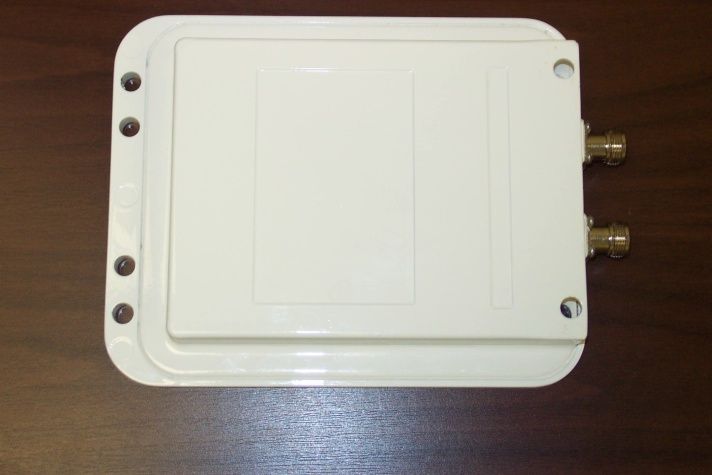
OQCWAF24-1000LWireless LAN Card with amplifier
Winncom Technologies Inc.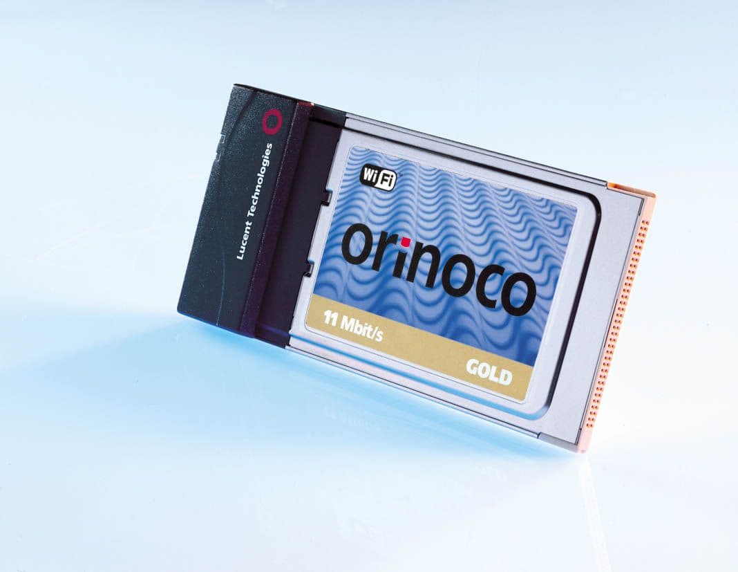
Click to zoom
Application Details
- Equipment Class
- DSS - Part 15 Spread Spectrum Transmitter
- Date of Grant
- Jun 28, 2001
- Application Purpose
- Original Equipment
- Date of Application
- Jan 05, 2001
- Equipment Note
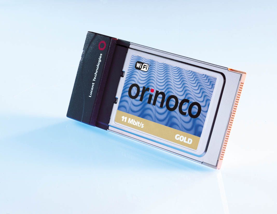
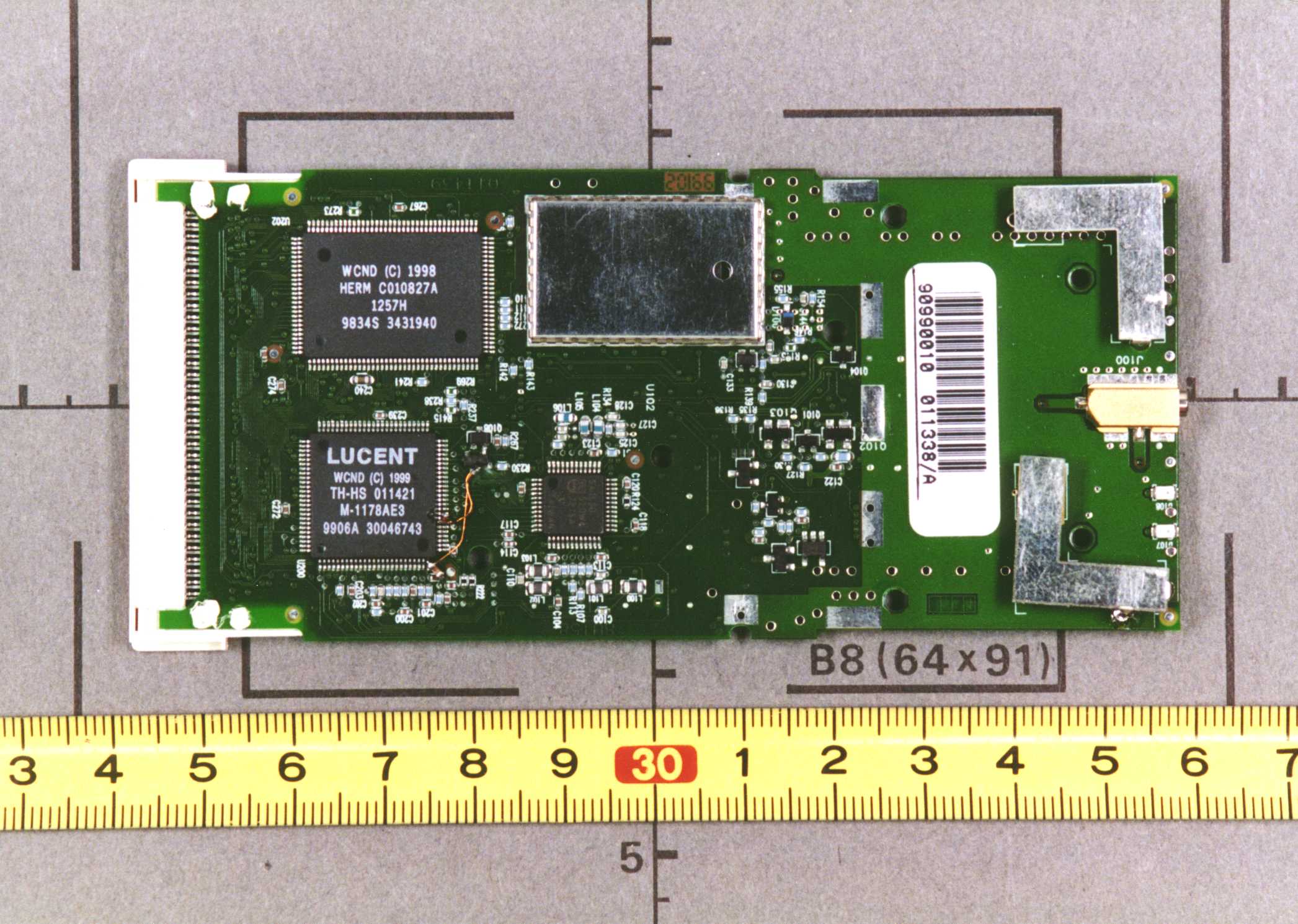
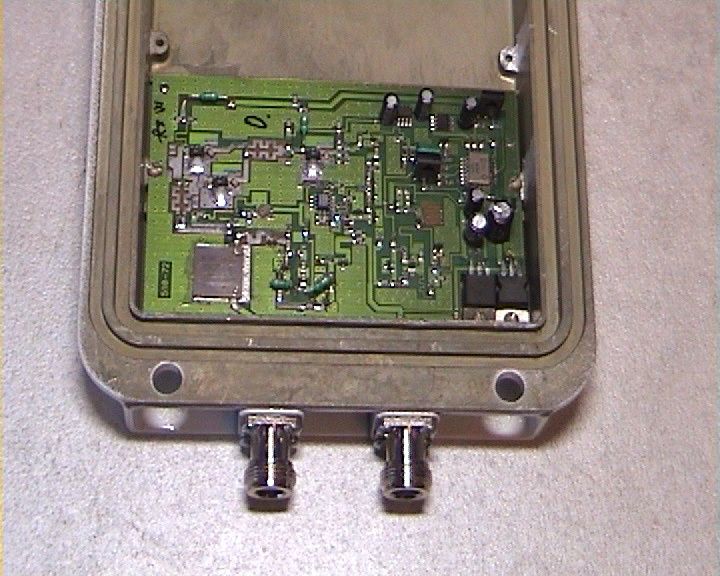
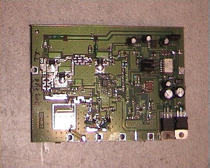
- Wireless LAN Card with amplifier
- Frequency Range
- 2412.00000000 - 2462.00000000
- Company
- Winncom Technologies Inc.
- Country
- United States
Documents & Files
Document Text
Text extracted from the exhibit documents filed with the FCC. Open a document above to read the original.
Users Manual
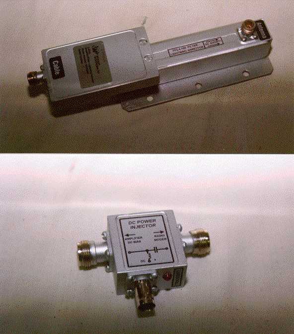
1 Product code WAF2400-1000L Antenna Amplifier, 2.4-2.4835 GHz, 0.250 W Output Caution: For use only with the provided Lucent Technologies ORiNOCO Model: PC24E-00-FC WaveLAN 2.4 GHz wireless card with FCC ID: IMRWLPC24. Use of other radio transmitters with this amplifier may cause interference, and is a violation of FCC Rules. The bi-directional RF amplifier greatly increases usable signal transmission range by increasing receiver sensitivity and compensating for various line losses (in the feeder, connectors and cable) and signal losses due to electromagnetic radiation. Receiver Performance Maximum Gain: 22dB Noise Figure: 2.8 dB Frequency Response: +/- 0.5 dB over operating range Output Saturation RF Power: 10 mW Transmitter Performance Automatic Gain Control Maximum Gain: 30 dB Intput RF Power: 0.5 - 100 mW Maximum Output RF Power: 250 mW Input/Output Impedance: 50 Ohm Switching Power: 0.2 - 0.4 mW Switch Delay Time: 0.5 - 0.8 mks Input/Output Connectors: N – Type Female Operating Temperature: -50°C - +50°C Power Supply Specifications Input Voltage: 110 - 240 VAC 50/60 Hz Output Voltage/Power: 12 VDC / 10 W DC Power Injector: - Radio Modem Connector: N – Type Female - Amplifier Connector: N – Type Female - 12 VDC Power Input Connector: BNC - Type Female Filter Specifications Filter Bandwidth: 100 MHz RF Range: 2.4 - 2.5 GHz Insertion Loss in 2.4-2.5 GHz: 0.5 dB Signal Attenuation: 50 dB @ 2 GHz Signal Attenuation: 50 dB @ 3 GHz Physical Characteristics Amplifier Weight: 2.0 lbs (0.9 kg) Amplifier Dimensions: 12 in x 4.8 in x 2.8 in (300mm x 120mm x 70mm) Power Supply Weight: 1.0 lb (0.45 kg) Power Supply Dimensions: 12 in x 4.8 in x 2.8 in (300mm x 120mm x 70mm) 2 FCC Notice: Use of RF amplifiers in the United States is subject to FCC regulations. This device cannot be used with any transmitter other than the one it has been supplied with. This device requires professional installation. User is responsible for compliance with applicable laws and regulations Installation and Operation Manual The entire transceiver station assembly consists of seven main components: 1.Low-noise receive amplifier, transmit amplifier, bandpass filter, and switching control unit assembled in a sealed enclosure. 2. DC power injector. The power injector connects to the transmitting device and the amplifier assembly with a 10 ft. RF 50 Ohm coaxial cable. 3. 110-220 VAC Power supply with DC output BNC connector. 4. 10 ft. 50 ohm RF cable assembly. 5. One of 4 antenna models (omni, yagi, dish) as appropriate for installation. 6. Lucent Technologies Model: PC24E-00-FC WaveLAN 2.4 GHz wireless PCMCIA card. 7. Computer system. The amplifier kit contains the following equipment: ItemQuantity Amplifier1 DC Power injector1 Power supply1 Mounting brackets1 U-bolt1 Installation Instructions Important Notice: Read the following installation instructions and all warnings carefully prior to installing the amplifier. Failure to follow installation instructions or tampering with the amplifier or the power supply will void the warranty. 3 1. Install the amplifier on a mast near the external antenna, using a U-shaped bracket (included). The amplifier can be installed vertically or horizontally. 2. Connect the side of the amplifier labeled “Modem” to the DC power injector, and the side labeled “Antenna” to a surge protector (not included) with the 10 ft., 50 Ohm coaxial cable. Important: In order for the amplifier to operate properly, and to avoid damage to the amplifier and the power supply, the maximum input power to the amplifier must not exceed 100mW. User must check for proper attenuation. 3. Connect the DC power injector to the external antenna port of the wireless modem card via a 50 Ohm coaxial jumper cable (included). 4. Following installation, a weather sealant must be applied to all external connectors to protect them from moisture (moisture can cause increased signal losses in the feeder, diminished transmission quality, and possible damage to the connectors and the amplifier). 5. Grounding. Ensure that the mounting mast is properly grounded. Check the ground on the amplifier assembly with a Ω-meter. 4 Warning: Improper grounding can adversely affect amplifier performance and may lead to equipment damage or personal injury. Failure to properly ground the amplifier will void the warranty. The amplifier does not have built-in surge protection, and is not designed to withstand a lightning strike. Use of a surge protector is highly recommended for outdoor installations. Amplifier warranty does not cover damage caused by lightning or static electricity. Operation of the Amplifier • On power up, the amplifier will be in a "receive" mode. The mode switches to "transmit" when the amplifier receives a signal from a radio modem. A Green light on the DC injector indicates that the amplifier has power. A red light on the DC injector indicates that the amplifier is in a "transmit" mode. The red light blinks when the amplifier is connected to a bi-directional RF device. • A constant red light indicates that the amplifier is continuously in "transmit" mode and is not communicating properly. This is an abnormal condition that can be caused by any of the following: - High noise level in the feeder of the transmitting device. With time, some radio modems develop elevated natural noise levels, even in the "receive" mode. This noise can cause the amplifier to switch from "receive" to "transmit" mode, causing interruptions in communications. If this problem is detected, the transmitting device should be replaced. - External interference. If the amplifier is not properly grounded, external interference can cause the amplifier to intermittently switch to "transmit" mode. This condition has been observed with some radio modems, due to the modems' poor shielding characteristics. Thus, if the transmitting device is not adequately shielded, several such devices operating in close proximity can interfere with the amplifier's operation. • If t…
Text truncated - open the document above for the full version.
Attestation Statements
Nederland B.V. Zadelstede 1-10 3431 JZ Nieuwegein The Netherlands Phone: +31 30 6097666 Fax: +31 30 6097556 FCC... Nieuwegein, 27 September 2000 Re: Processing Gain WaveLAN PC Cards - For Chip/symbol rate etc. see the table below: Bit rateChip/symbol rateBit/symbol rateChip/bit rate 1 Mbit/sec111, DBPSK11 2 Mbit/sec112, DQPSK5.5 5.5 Mbit/sec84, CCK2 11 Mbit/sec88, CCK1 Sincerely yours, Bert Vos, Certifications Support, Email: [email protected] Encl. cc:
Block Diagram
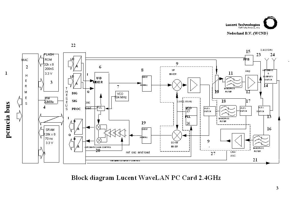
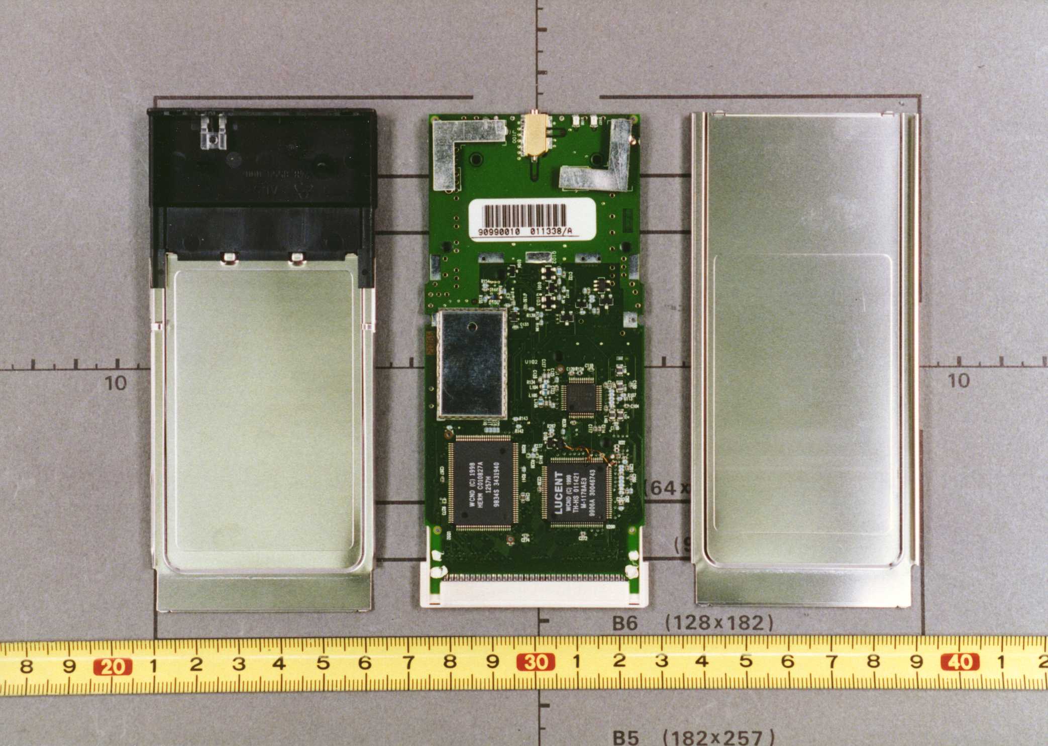
Block diagram description of the Lucent WaveLAN PC Card 2.4GHz, High Speed 1 WaveLAN PC Card 2.4 GHz High Speed DESCRIPTION OF THE BLOCK DIAGRAM The various parts of the Block diagram are numbered and an explanation is given of these blocks. First the transmitter will be described: A) Digital Signal Processor. (22) Function : Generate spreaded signal with an Barker sequence of 11, the original raw data rate of 1, 2, 5.5 or 11 Megabits is transformed to a symbol rate of one MegaBaud and multiplied with eleven and modulated with a DQPSK ( Differential Quadrature Phase Shift Keying ) Modulation for 1 and 2 Mbps or DQPSKCCK (CCK = Complementary Code Keying) for 5.5 and 11 Mbps. The unfiltered data comes out of I and Q and goes to the up/down mixer (6) B) The above signals are mixed in (6) in a so called quadrature modulator with the Intermediate Frequency ( IF) of 352 MHz. C) The upmixer is fed by the VCO of 704 MHz, which is divided by 2 to 352 MHz. D) The SAW ( 8 ) filters all unwanted mixing products, such that only the 352 MHz band remains. E) This signal goes into the RF upmixer ( 9) SA2420 were it is mixed with the RF VCO with a range of 2050 to 2150 MHz. F) The Rx/Tx switch (17) brings the signal to the variable attenuator (10 ), where the output level is controlled. G) The signal is fed through a 2.4- 2.5 GHz bandpass filter (11) to remove all unwanted mixer products, and thus to get a clean signal for further processing. H) The signal is amplified in (12), with approx 23 dB to an output level of approx. 15 dBm I) This signal goes to the RX/TX antenna (23/24) via the special connector with a switch inside to disable the antenna. J) The output power is controlled with a so called power feed back loop (15) in which the output power is compared with a DAC value from (10) Receiver functions. K) The receive signal enters the antenna passes the RX/TX switch (14) and (13) this is set to RX mode. L) The signal goes through the 2.4 GHz filter (16) to remove all unwanted spectral components in order to deliver a clean signal for the receiver. M) A Low Noise Amplifiers (LNA) (in 9) is used to amplify the weak signal to a level fitted for down mixing. N) The AGC (27) can amplify or attenuate the signal according to the Digital signal processor required input with a step size of 26 dB. O) Again the Rx/Tx switch in the Rx mode is passed and also the same filter as in transmit mode ( 18). P) The down mixer (9) mixes the 2.4 GHz with the 2.1 GHz to the 352 MHz IF. Q) The signal of 352 MHz is amplified again (9) and filtered by a SAW filter (19) to give a clean signal for the second mixer. Block diagram description of the Lucent WaveLAN PC Card 2.4GHz, High Speed 2 R) The Downmixer (6) mixes the 352 MHz signal down to the I and Q signals, also the auto gain control can increase the level to the required level via line 20. S) The very low amplitude baseband I and Q signal is amplified in the AMPs (6) to a level fitted for the Analog to Digital converters (22), which make it a proper signal for the digital signal processor. T) The digital signal processor (22) removes the spreading as present on the signal with a so called autocorrelation function. The resulting output of the processor is a received data rate of 1, 2, 5.5 or 11 Megabits. VCO , PLL and OSC. U) These three form one entity to generate a single tone signal for down mixing. There are two of these blocks available, one for the IF LO (7 and 6 ) (352MHz ) and one for the RF LO (25 and 26) of 2050 to 2150 MHz. V) All the PLL’s and the processor (2) have one reference Crystal of 22 MHz (4) with an accuracy of 25 ppm. General circuits: W) Antenna Diversity. This functin may be placed on the radio board or on extended board (as part of external antenna. Depending on the signal strength and signal quality the Digital processor (22) can choose between the two antenna’s (23) and (24) which gives the best signal. This is done initial during the training sequence in the received signal. X) Automatic Gain control. Depending on the signal strength and signal quality the Digital processor (22) can choose to increase or decrease the signal level at the digital input, this is done by reducing or increasing the gain in the receiver via the LNA-AGC (in 9). Y) The Signal processor (22) can read via the MAC (2) the registers for programming all parameters for transmit/receive functions Z) The MAC is used to do the handshaking with the PCMCIA bus (1 ) and handling the IEEE protocol. Also used to load the PLL frequencies and dividers, also used to interface to the FlashROM which contains all parameters for the PLL’s and the Callcode. AA) Not shown is the regulator to supply the 3.3 Volt out of the 5 Volt out of the PCMCIA Bus (1) Guus Jansen Rev. A 12Apr99/BVos Block diagram description of the Lucent WaveLAN PC Card 2.4GHz, High Speed 3 INDICATION MAIN PARTS Rev. A 12Apr99/BVos 2: HERMES 3. AT29C010 4 CDFDCJ2 5. KM68V1000 6. SA1630 7. MQE 901-704 8 + 19. L545D 9. SA2420 11 + 18. LFSN30N17C2450B 12. BFP420 + BFP450 13 + 17. BAR63 14. BAR80 16. LFJ30-07B2450 22. THESEUS-HS (High Sped) 25. MQG101-2098 26. UMA1021
ID Label/Location Info
FCC LABEL FORMAT AND LOCATION TOP VIEW Winncom Technologies, Inc. FCCID: OQCWAF24-1000L This device complies with Part 15 of the FCC Rules. Operation of this device is subject to the Following conditions: (1) This device may not cause harmful interference, and (2) this device must accept any interference received, including interference that may cause undesired operation. Winncom Technologies, Inc. FCCID: OQCWAF24-1000L This device complies with Part 15 of the FCC Rules. Operation of this device is subject to the Following conditions: (1) This device may not cause harmful interference, and (2) this device must accept any interference received, including interference that may cause undesired operation.
Operational Description
Block diagram description of the Lucent WaveLAN PC Card 2.4GHz, High Speed 1 WaveLAN PC Card 2.4 GHz High Speed DESCRIPTION OF THE BLOCK DIAGRAM The various parts of the Block diagram are numbered and an explanation is given of these blocks. First the transmitter will be described: A) Digital Signal Processor. (22) Function : Generate spreaded signal with an Barker sequence of 11, the original raw data rate of 1, 2, 5.5 or 11 Megabits is transformed to a symbol rate of one MegaBaud and multiplied with eleven and modulated with a DQPSK ( Differential Quadrature Phase Shift Keying ) Modulation for 1 and 2 Mbps or DQPSKCCK (CCK = Complementary Code Keying) for 5.5 and 11 Mbps. The unfiltered data comes out of I and Q and goes to the up/down mixer (6) B) The above signals are mixed in (6) in a so called quadrature modulator with the Intermediate Frequency ( IF) of 352 MHz. C) The upmixer is fed by the VCO of 704 MHz, which is divided by 2 to 352 MHz. D) The SAW ( 8 ) filters all unwanted mixing products, such that only the 352 MHz band remains. E) This signal goes into the RF upmixer ( 9) SA2420 were it is mixed with the RF VCO with a range of 2050 to 2150 MHz. F) The Rx/Tx switch (17) brings the signal to the variable attenuator (10 ), where the output level is controlled. G) The signal is fed through a 2.4- 2.5 GHz bandpass filter (11) to remove all unwanted mixer products, and thus to get a clean signal for further processing. H) The signal is amplified in (12), with approx 23 dB to an output level of approx. 15 dBm I) This signal goes to the RX/TX antenna (23/24) via the special connector with a switch inside to disable the antenna. J) The output power is controlled with a so called power feed back loop (15) in which the output power is compared with a DAC value from (10) Receiver functions. K) The receive signal enters the antenna passes the RX/TX switch (14) and (13) this is set to RX mode. L) The signal goes through the 2.4 GHz filter (16) to remove all unwanted spectral components in order to deliver a clean signal for the receiver. M) A Low Noise Amplifiers (LNA) (in 9) is used to amplify the weak signal to a level fitted for down mixing. N) The AGC (27) can amplify or attenuate the signal according to the Digital signal processor required input with a step size of 26 dB. O) Again the Rx/Tx switch in the Rx mode is passed and also the same filter as in transmit mode ( 18). P) The down mixer (9) mixes the 2.4 GHz with the 2.1 GHz to the 352 MHz IF. Q) The signal of 352 MHz is amplified again (9) and filtered by a SAW filter (19) to give a clean signal for the second mixer. Block diagram description of the Lucent WaveLAN PC Card 2.4GHz, High Speed 2 R) The Downmixer (6) mixes the 352 MHz signal down to the I and Q signals, also the auto gain control can increase the level to the required level via line 20. S) The very low amplitude baseband I and Q signal is amplified in the AMPs (6) to a level fitted for the Analog to Digital converters (22), which make it a proper signal for the digital signal processor. T) The digital signal processor (22) removes the spreading as present on the signal with a so called autocorrelation function. The resulting output of the processor is a received data rate of 1, 2, 5.5 or 11 Megabits. VCO , PLL and OSC. U) These three form one entity to generate a single tone signal for down mixing. There are two of these blocks available, one for the IF LO (7 and 6 ) (352MHz ) and one for the RF LO (25 and 26) of 2050 to 2150 MHz. V) All the PLL’s and the processor (2) have one reference Crystal of 22 MHz (4) with an accuracy of 25 ppm. General circuits: W) Antenna Diversity. This functin may be placed on the radio board or on extended board (as part of external antenna. Depending on the signal strength and signal quality the Digital processor (22) can choose between the two antenna’s (23) and (24) which gives the best signal. This is done initial during the training sequence in the received signal. X) Automatic Gain control. Depending on the signal strength and signal quality the Digital processor (22) can choose to increase or decrease the signal level at the digital input, this is done by reducing or increasing the gain in the receiver via the LNA-AGC (in 9). Y) The Signal processor (22) can read via the MAC (2) the registers for programming all parameters for transmit/receive functions Z) The MAC is used to do the handshaking with the PCMCIA bus (1 ) and handling the IEEE protocol. Also used to load the PLL frequencies and dividers, also used to interface to the FlashROM which contains all parameters for the PLL’s and the Callcode. AA) Not shown is the regulator to supply the 3.3 Volt out of the 5 Volt out of the PCMCIA Bus (1) Guus Jansen Rev. A 12Apr99/BVos Block diagram description of the Lucent WaveLAN PC Card 2.4GHz, High Speed 3 INDICATION MAIN PARTS Rev. A 12Apr99/BVos 2: HERMES 3. AT29C010 4 CDFDCJ2 5. KM68V1000 6. SA1630 7. MQE 901-704 8 + 19. L545D 9. SA2420 11 + 18. LFSN30N17C2450B 12. BFP420 + BFP450 13 + 17. BAR63 14. BAR80 16. LFJ30-07B2450 22. THESEUS-HS (High Sped) 25. MQG101-2098 26. UMA1021
Operational Description
Block diagram description of the Lucent WaveLAN PC Card 2.4GHz, High Speed 1 WaveLAN PC Card 2.4 GHz High Speed DESCRIPTION OF THE BLOCK DIAGRAM The various parts of the Block diagram are numbered and an explanation is given of these blocks. First the transmitter will be described: A) Digital Signal Processor. (22) Function : Generate spreaded signal with an Barker sequence of 11, the original raw data rate of 1, 2, 5.5 or 11 Megabits is transformed to a symbol rate of one MegaBaud and multiplied with eleven and modulated with a DQPSK ( Differential Quadrature Phase Shift Keying ) Modulation for 1 and 2 Mbps or DQPSKCCK (CCK = Complementary Code Keying) for 5.5 and 11 Mbps. The unfiltered data comes out of I and Q and goes to the up/down mixer (6) B) The above signals are mixed in (6) in a so called quadrature modulator with the Intermediate Frequency ( IF) of 352 MHz. C) The upmixer is fed by the VCO of 704 MHz, which is divided by 2 to 352 MHz. D) The SAW ( 8 ) filters all unwanted mixing products, such that only the 352 MHz band remains. E) This signal goes into the RF upmixer ( 9) SA2420 were it is mixed with the RF VCO with a range of 2050 to 2150 MHz. F) The Rx/Tx switch (17) brings the signal to the variable attenuator (10 ), where the output level is controlled. G) The signal is fed through a 2.4- 2.5 GHz bandpass filter (11) to remove all unwanted mixer products, and thus to get a clean signal for further processing. H) The signal is amplified in (12), with approx 23 dB to an output level of approx. 15 dBm I) This signal goes to the RX/TX antenna (23/24) via the special connector with a switch inside to disable the antenna. J) The output power is controlled with a so called power feed back loop (15) in which the output power is compared with a DAC value from (10) Receiver functions. K) The receive signal enters the antenna passes the RX/TX switch (14) and (13) this is set to RX mode. L) The signal goes through the 2.4 GHz filter (16) to remove all unwanted spectral components in order to deliver a clean signal for the receiver. M) A Low Noise Amplifiers (LNA) (in 9) is used to amplify the weak signal to a level fitted for down mixing. N) The AGC (27) can amplify or attenuate the signal according to the Digital signal processor required input with a step size of 26 dB. O) Again the Rx/Tx switch in the Rx mode is passed and also the same filter as in transmit mode ( 18). P) The down mixer (9) mixes the 2.4 GHz with the 2.1 GHz to the 352 MHz IF. Q) The signal of 352 MHz is amplified again (9) and filtered by a SAW filter (19) to give a clean signal for the second mixer. Block diagram description of the Lucent WaveLAN PC Card 2.4GHz, High Speed 2 R) The Downmixer (6) mixes the 352 MHz signal down to the I and Q signals, also the auto gain control can increase the level to the required level via line 20. S) The very low amplitude baseband I and Q signal is amplified in the AMPs (6) to a level fitted for the Analog to Digital converters (22), which make it a proper signal for the digital signal processor. T) The digital signal processor (22) removes the spreading as present on the signal with a so called autocorrelation function. The resulting output of the processor is a received data rate of 1, 2, 5.5 or 11 Megabits. VCO , PLL and OSC. U) These three form one entity to generate a single tone signal for down mixing. There are two of these blocks available, one for the IF LO (7 and 6 ) (352MHz ) and one for the RF LO (25 and 26) of 2050 to 2150 MHz. V) All the PLL’s and the processor (2) have one reference Crystal of 22 MHz (4) with an accuracy of 25 ppm. General circuits: W) Antenna Diversity. This functin may be placed on the radio board or on extended board (as part of external antenna. Depending on the signal strength and signal quality the Digital processor (22) can choose between the two antenna’s (23) and (24) which gives the best signal. This is done initial during the training sequence in the received signal. X) Automatic Gain control. Depending on the signal strength and signal quality the Digital processor (22) can choose to increase or decrease the signal level at the digital input, this is done by reducing or increasing the gain in the receiver via the LNA-AGC (in 9). Y) The Signal processor (22) can read via the MAC (2) the registers for programming all parameters for transmit/receive functions Z) The MAC is used to do the handshaking with the PCMCIA bus (1 ) and handling the IEEE protocol. Also used to load the PLL frequencies and dividers, also used to interface to the FlashROM which contains all parameters for the PLL’s and the Callcode. AA) Not shown is the regulator to supply the 3.3 Volt out of the 5 Volt out of the PCMCIA Bus (1) Guus Jansen Rev. A 12Apr99/BVos Block diagram description of the Lucent WaveLAN PC Card 2.4GHz, High Speed 3 INDICATION MAIN PARTS Rev. A 12Apr99/BVos 2: HERMES 3. AT29C010 4 CDFDCJ2 5. KM68V1000 6. SA1630 7. MQE 901-704 8 + 19. L545D 9. SA2420 11 + 18. LFSN30N17C2450B 12. BFP420 + BFP450 13 + 17. BAR63 14. BAR80 16. LFJ30-07B2450 22. THESEUS-HS (High Speed) 25. MQG101-2098 26. UMA1021
Operational Description
NEDERLAND B.V. May99 DESCRIPTION WAVELAN IEEE PC Card Extended High Speed (FCC) This WAVELAN IEEE PC Card product provides a WaveLAN compatible wireless connection for portable and mobile computers in accordance with IEEE standard 802.11 DSSS. It can work at 11, 5.5, 2 or 1 Mbps. The operation is in accordance with IEEE 802.11. The product, one piece of hardware, contains the following blocks: - PCMCIA interface - Wireless Medium Access Control (WMAC); this chip is used for handshaking with the PCMCIA bus and for handling the IEEE protocol; it also does frequency management and interfaces to FlashROM for parameters on frequencies and Call codes. Here also selection for 11, 5.5, 2 or 1 Mbps is handled. - Digital signal processor takes care of all modulation/demodulation for DSSS for all above rates and can do selection out of 2 receiving antennae - Antenna function, provides a diversity antenna and connection to optional external antenna. It provides two antenna elements, one for transmitting while one of the two can be selected for reception. Optionally it can be equipped with: - a factory installable data encryption feature (WEP), and - a BootROM for diskless workstation. Block Diagram PCMCIA Interface Connector The technical specification is as follows on the next page. Antenna Conn . WMAC DIGITAL SIGNAL PROCESSOR NEDERLAND B.V. May99 TECHNICAL SPECIFICATION WAVELAN IEEE PC Card Extended High Speed (FCC) 2.4 GHz Data Signalling Rate:11, 5.5, 2 or 1 Mbit/s Media Access Protocol:According to IEEE 802.11 DSSS, CSMA/CA (Collision Avoidance) Bit Error Rate:Better than 10-8 Base-Band Modulation:- 2 Mbps: Differential Quadrature Phase Shift (before spreading) Keying (DQPSK) 2 bits/symbol - 11 and 5.5 Mbps: Complementary Code Keying Differential Quadrature Phase Shift Keying (DQPSK CCK) Spread Spectrum:Direct Sequence with 11 chips/symbol interval. Pseudo random Barker code sequence: { 1 -1 1 1 -1 1 1 1 -1 -1 -1 } Chipping Rate: 11 Mchips/s Carrier Frequency:Selectable from factory pre-programmed set according to IEEE 802.11: 2412, 2417, 2422, 2427, 2432, 2437, 2442, 2447, 2452, 2457 and 2462 MHz Peak Output Power:< 32 mW rms power (15 dBm) RF Power Density:< 8 dBm/3kHz Antenna (indoor):Omni-Directional (integrated): - Gain 0 dBi - Polarization diversity Hor/Vert External, e.g. Range Extender AIN24-OD-0202: - Gain 0 dBi - Polarization diversity Hor/Vert. Spurious Emissions etc:Satisfies the USA Federal Comm. Commission (FCC) rules Part 15.247
RF Exposure Info
RF Exposure Calculations: The following information provides the minimum clearance distance for the various antennas provided with the Winncom Technologies AMP250 system, as calculated from FCC OET 65 Appendix B, Table 1B Guidlines for General Population/Uncontrolled Exposure. This calculation is based on the highest EIRP possible from the system, considering maximum power and antenna gain. The formula used was: S = (Po*G)/(4*pi*r^2) Where S = 1.0 mW/cm^2 for 2400 MHz. Where Po = 250 mW max. --------------------------------------------- The following statement will be presented in the AMP250 User Manual: WARNING In order to comply with FCC adopted RF Exposure Requirements, the included antenna must be installed in a manner that will provide clearance from the antenna, to any personnel or member of the public, according to the following guide: WRO2400-70 - 7dBi Omni - 20 cm WRO2400-125 - 12.5 dBi Omni - 20 cm HGY15 - 13.5 dBi Yagi - 21 cm WRO2400-24 - 24 dBi Grid Dish - 71 cm For: 7 dBi Omni Antenna - Winncom Model WRO2400-70 .... r = 10 cm Antenna Description: 23 inch omni whip For: 12.5 dBi Omni Ant. - Winncom Model WRO2400-125 .. r = 19 cm Antenna Description: For: 13.5 dBi Yagi Ant. - Winncom Model HGY15 . . . . . r = 21 cm Antenna Description: For: 24 dBi Dish Ant. - Model WRO2400-125 . . . r = 71 cm Antenna Description: Grid Size: 42 inches X 24 inches Dipole Length: 14 inches
Test Report
RF Measurement Report Prepared by: NATIONAL CERTIFICATION LABORATORY 8370 Court Avenue, Suite B-1 Ellicott City MD 21043 (410) 461-5548 In Support of: FCC APPLICATION FOR CERTIFICATION for Winncom Technologies, Inc. 30700 Carter Street, Suite A Solon, OH 44139 Model: Lucent PC24E-00-FC WaveLAN with AMP250 Amplifier FCC ID: OQCWAF24-1000L Demonstration of Compliance with FCC Rules Part 15.247 January, 2001 FCC ID #: OQCWAF24-1000L 2 TABLE OF CONTENTS Application Form 731 FCC Label Drawing and Location 1.0 Introduction 1.1 Summary 2.0 Description of Equipment Under Test (EUT) 3.0Test Program 4.0Test Configuration 5.0 Conducted Emissions Scheme 6.0 Radiated Emissions Scheme TABLES Table 1.EUT Accessories Table 2.Support Equipment Table 3. Measurement Equipment EXHIBITS Exhibit 1.EUT Photographs Exhibit 2. Schematic Diagram Exhibit 3. User Manual NCL PROJ.# WINCOMM-0526B FCC ID #: OQCWAF24-1000L 3 1.0 Introduction This report has been prepared on behalf of Winncom Technologies, Inc., to support the attached Application for Certification of a Part 15 Spread Spectrum Transmitter. The Equipment Under Test was the Model Lucent PC24E-00-FC WaveLAN with AMP250 Amplifier. Radio-Noise Emissions tests were performed according to FCC Public Notice 54797, titled "Guidance on Measurements for Direct Sequence SST". The measuring equipment conforms to ANSI C63.2 Specifications for Electromagnetic Noise and Field Strength Instrumentation. Testing was performed at National Certification Laboratory in Ellicott City, MD. Site description and site attenuation data have been placed on file with the FCC's Sampling and Measurements Branch. FCC acceptance was granted on May 26, 1993. 1.1 Summary The Winncom Technologies, Inc. Model Lucent PC24E-00-FC WaveLAN with AMP250 Amplifier complies with the FCC limits (15.247) for a Direct Sequence SST. 2.0 Description of Equipment Under Test (EUT) The Lucent PC24E-00-FC WaveLAN is actually the FCC Certified PCMCIA Model with FCC ID: IMRWLPC24. Winncom Technologies, Inc. has not modified this product in any manner except for the addition of high gain antennas, and an external amplifier. The EUT Features: Direct Sequence Spread Spectrum Transceiver + 24 dBm RF Output Max. 2412 to 2462 MHz Freq. Range 10 MHz 6 dB Emission Bandwidth 10 Available Channels 5 MHz Channel Separation 11 Mbps Data Rate (Radio Link) Differential DPSK Modulation FCC ID #: OQCWAF24-1000L 4 3.0 Test Program This report contains measurement charts and data as evidence for the following tests performed: 1. (15.247 b) Peak RF output power. 2. (15.247 d) Power Spectral Density (3kHz Bandwidth). 3. (15.247 c) Field strength of harmonics and spurious out-of-band emissions. 4. (15.247 c) RF Antenna Conducted of harmonics and spurious out-of-band emissions. 5. (15.247 a) 6 dB Emission Bandwidth. 6. (15.207) Power Line Conducted Emissions. 4.0 Test Configuration The Lucent PC24E-00-FC WaveLAN was installed in a KDS Valient 5000 Laptop computer for testing. A Win98 Hyperterminal program is used to control the transmitter. The external amplifier is connected in-line between the wireless bridge and antenna via 10 feet of low loss cable. The 10 foot cable is the minimum length supplied with the system. RF power output measurements were taken with an RF power meter at the amplifier output connecter after the 10 ft. cable. RF antenna conducted output tests such as Bandwidth, Spurious/Harmonics, and Power Spectral Density were taken with the amplifier ouput feeding directly into the spectrum analyzer via the 10 ft. cable. The …
Text truncated - open the document above for the full version.
Contact Information
Applicant
Michael P. Maly(Executive Vice President)
Technical Contact
National Certification LabBrian Haghtalab
[email protected]410 461 5548
8370 Court Ave. · Ellicott City, Maryland · United States
Non-Technical Contact
National Certification LabBrian Haghtalab
410 461 5548
Test Firm
National Certification LaboratoryBrian Haghtalab
Technical Specifications
| # | Rule Parts | Frequency Range | Power Output |
|---|---|---|---|
| 1 | 15C | 2.41 GHz - 2.46 GHz | 250.00 mW |
Other Applications from Winncom Technologies Inc.
OQCWAF24-1000
Jun 07, 2000DSS - Part 15 Spread Spectrum Transmitter
Equipment Class
DSS - Part 15 Spread Spectrum Transmitter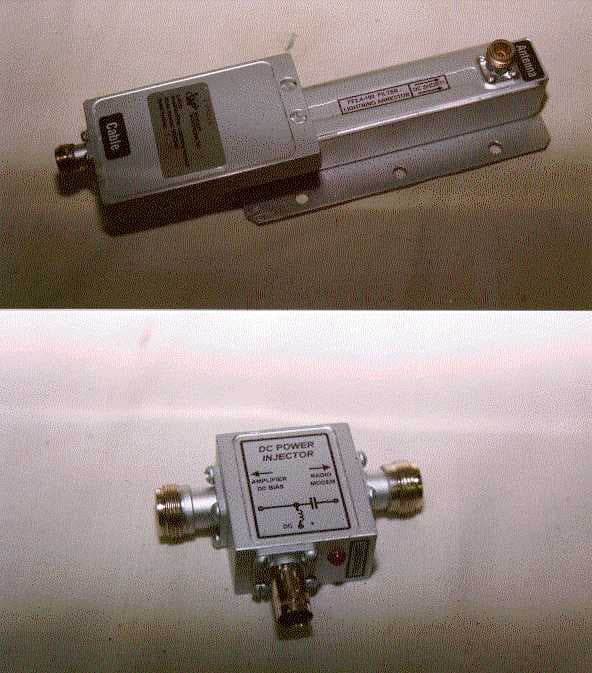
OQCWAF24-250
Jun 07, 2000DSS - Part 15 Spread Spectrum Transmitter
Equipment Class
DSS - Part 15 Spread Spectrum Transmitter