OTHN-9000MWD900MHz DSSS Cordless Phone System
Tele Matrix Equipment, LLC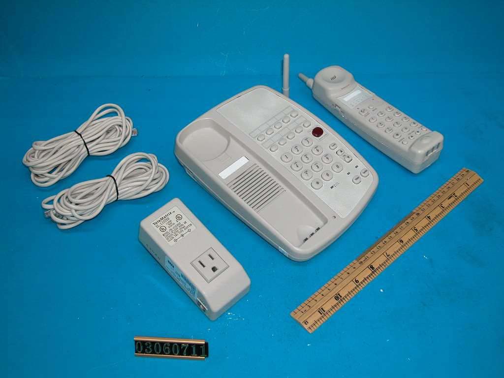
Click to zoom
Application Details
- Equipment Class
- DTS - Digital Transmission System
- Date of Grant
- Aug 13, 2003
- Application Purpose
- Original Equipment
- Date of Application
- Aug 13, 2003
- Equipment Note
- 900MHz DSSS Cordless Phone System
- Frequency Range
- 904.20000000 - 925.80000000
- Company
- Tele Matrix Equipment, LLC
- Country
- United States
Documents & Files
Document Text
Text extracted from the exhibit documents filed with the FCC. Open a document above to read the original.
Block Diagram
PDF created with FinePrint pdfFactory Pro trial version http://www.fineprint.com
External Photos
External photos FCC ID: OTH-9000MWD External photos FCC ID: OTH-9000MWD
ID Label/Location Info
LABEL ETL LABEL SNO LABEL FCC LABEL WARRANTY 9000 SERIES BOTTOM LABEL LOCATION DESCRIPTIONDATEISSUE 46.20 1 4 . 2 0 0.10 ADHESIVE +0.00 -0.10 + 0 . 0 0 - 0 . 1 0 MADE IN CHINA GALAXY Drawn : Checked Approved Description Part No. Model No. Material Treatment Tolerances Unless otherwise Specified Unit : mmScale :Projection: 3rd Ang. Commutech Limited A4 : : 2 : 1 : PAPER : 110-1776-1 : 9000MWD : LABEL-FCC BASE 9000MWD 2003.1.8 NOTE: 2. PAPER COLOR: WARM GRAY 2C.. 3. TEXT COLOR: WARM GRAY 10C. 1. MATERIAL: PAPER. COMPLIES WITH 47 CRF PART 68 TECHNICAL REQUIREMENTS REG. NO.: US: 2N3WI29B95339 FCC ID: OTHN-9000MWD RINGER EQUIVALENCE: 2.9B USOC JACK: RJ11C 9000MWD MODEL NO.: 95339 HAC TeleMatrix,Inc. GALAXY Drawn Checked Approved Description Part No. Model No. Material : Treatment : Tolerances Unless otherwise Specified Unit : mmScale :Projection: 3rd Ang. Commutech Limited A4 DESCRIPTIONDATEISSUE : : : NOTE: 2. PAPER COLOR: WARM GRAY 2C. 3. TEXT COLOR: WARM GRAY 10C. 1. MATERIAL: PAPER. 2 : 1 0.10 ADHESIVE PAPER : 110-1777 : 9000MWD 45.00 3 0 . 0 0 03.3.29 TeleMatrix, Inc. Part 15 Compliance This device complies with Part 15 of the FCC Rules. Operation is subject to the following two conditions: (1)This device may not cause harmful interference, and (2) This device must accept any interference received, Including interference that may cause undesired operation. Privacy of communications may not be ensured when using this phone. INFORMATION TECHNOLOGY EQUIPMENT US 9700163 R Licensed under United States Patent No. 5,263,084 MODEL NO.:95339 : LABEL-ETL 9000MWD FCC LABEL LOCATION ON H/S 9000MWD FCC LABEL LOCATION ON HANDSET DESCRIPTIONDATEISSUE 0.10 ADHESIVE GALAXY Drawn : Checked Approved Description Part No. Model No. Material Treatment Tolerances Unless otherwise Specified Unit : mmScale :Projection: 3rd Ang. Commutech Limited A4 : : 2 : 1 : PAPER : 110-1826-1 : 9000MWD : LABEL-FCC ID ON H/S 9000MWD 2003.6.10 NOTE: 2. PAPER COLOR: WARM GRAY 2C. 3. TEXT COLOR: WARM GRAY 10C. 1. MATERIAL: PAPER. 25.00 mm 8 . 0 0 m m MADE IN CHINA 9000MWD MODEL NO.: 95339 TeleMatrix,Inc. FCC ID: OTHN-9000MWD
Internal Photos
Internal photos FCC ID: OTH-9000MWD Base assembly (View 1) Base assembly (View 2) Internal photos FCC ID: OTH-9000MWD Base Main PCB comp side Base Main PCB solder side Internal photos FCC ID: OTH-9000MWD Base keypad front side Base keypad rear side Internal photos FCC ID: OTH-9000MWD Base Oscillator PCB comp side Internal photos FCC ID: OTH-9000MWD Handset assembly Handset Main PCB comp side Internal photos FCC ID: OTH-9000MWD Handset keypad side Handset Oscillator PCB comp side
Operational Description
Galaxy Commutech Limited 1 of 3 Circuitry Description for 9000MWD Cordless Phone 1. Part of Cordless Phone 1) Handset RF signal sent from base unit is received by ANT1 antenna and passes through L3, C46, L8, C73, L4 and C74 and sends to U4 RF105- 12 IC for amplification and demodulation. Afterwards the signal is delivered to U1 R6753-14 (CPU) for D/A conversion and amplification. One path: output speech signal via R2 and R5 to SPK1, 150ohm receiver for sound reduction. The other path: ringer signal outputs from Pin 44 of U1 R6753-14 and is amplified via R54, Q1 to drive BU1 buzzer to sound. The speech signal picked up by MIC1 microphone sends to CPU U1 R6753-14 via R13, R14, R15, R16, R10, R11, C13 and C14 for amplification and A/D conversion and passes to U4 RF105-12 for RF modulating via R37, L10 and C56, then passes to U5 RF106-12 for RF power amplification via R49 and C69, then outputs the amplified RF modulation signal from Pin 1 and passes to ANT1 for sending out via L14, L7, L6, C47, D10, C46 and L3. Q2, Q3, L1, D10 and D11 form the TX/RX switching circuitry. U3 XC62GR3012 is voltage regulation IC for power supply. U2 93C66 is EEPROM IC. BAT1 is 3.6V battery power supply connected with each IC for use with J1 jack. 2) Cordless Part of Base Unit RF signal is received by ANT1 antenna from handset and passes through band-pass filter made up by L14, C171, L13, and C175 to U21 RF105-12 IC for receiving, amplification and demodulation. Afterwards the signal is delivered to U7 R6753-14 (CPU) for D/A switching and amplification then passes through U8 CD4066 to switch on/off, then uses T1 adaptor for coupling and sends to telephone line. Galaxy Commutech Limited 2 of 3 The sound signal from telephone line passes through U7 R6753-14 for A/D switching and amplification after T1 coupling and passes through U21 RF105-2 for RF modulation and amplification and passes through 15pin to R232, C163 and get into U23 RF-106-12 for RF amplification, then passes through wave falling loop made up by L9, L10, L11, L169, D43, C171 and L14 to ANT1 for sending out. Q44, Q45, D43 and D44 make up of TX/RX switching circuitry. U21 is frequency amplification IC. U22 XC62CTR3012 is voltage regulation IC. U13 93C66A is EEPROM. 2. Telephone Part 1) DC Power Circuit D6, D7, D9, D11 and 1N4004 make up of Polarity Protecting of DC Input to acquire +9VDC. U18 and 78L05 make up of +5V Voltage Regulation Circuit to supply the working voltage of complete unit. The Charge Circuit of Battery is made up of Q43, Q37, IN 3906 and Q42MPSW51, Q18 and IN3904. 2) Ring Circuit of Base Unit After input from TIP and RING of telephone line, provide over-voltage protection via FU1 and FU2, block (cut off) direct current with C183 1uF/250v capacitor and limit amplitude with ZD3 and ZD1, one circuit pass through U19, PC817 to make up of RF Ring Detection Circuit and activate the U7 R6753-14CPU to send out ring command to cordless handset; another circuit passes through D30, D31, D32, D33 and IN4004 to make up of polarity protecting circuit and get the positive and negative ring voltage, after voltage regulated with ZD12 24V zener diode, send to U5 GL6851 ring IC to ensure the base BUZ1 to ring. 3) Telephone Line Circuit of Base Unit Galaxy Commutech Limited 3 of 3 The current of wire TIP and RING pass through D13, D20, D24, D25 and IN4004 to made up of polarity protecting circuit after overvoltage/overcurrent protected by FU1, FU2, ZNR1 270V. One circuit is wireless communication circuit. ON/OFF HOOK circuit of which are made up of REY, Relay, Q16 and 2N3906. T1 and EI-24 coil as coupling coil can match with input/output impedance of phone. Another circuit is base unit communication circuit. ON/OFF HOOK circuits are made up of Q5, Q6, A92, Q7 and A42 and as the major circuit path of phone operation. 4) Dialing Circuit of Base Unit U1 KS57P 5208 is the kernel (key) circuit of the phone part which can implement dial, memory, and mute etc features. 5) Speaker Circuit of Base Unit U2 MC3321S (speaker IC) as base unit communication circuit can implement the input/output impedance switch and amplify dial. U4 CD4051A IC controls the volume control circuit of communication. The unit can be electrically adjusted to 8 steps in volume. Prepared By: F S Chen Date: June 5, 03
RF Exposure Info
Intertek Testing Services FCC ID: K7G2G4DSS24NS3 Date: June 18, 2003 For SAR evaluation of the handset, refer to TCB Exclusions List Revised on 17 July 2002. Transmitter with output power less than 60/fGHz (d < 2.5cm) can be certified by TCB without the SAR evaluation. In fact, the Output power for transmitters is the higher of the conducted or radiated (EIRP) source-based time-averaged output. And the fGHz is mid-band frequency in GHz, and d is the distance to a person’s body, excluding hands, wrists, feet, and ankles. For the tested model of 95339, Base unit: The measured peak conducted power was 2.21mW and the source-based time averaged output power was 0.99mW as TX duty cycle of the handset is 44.7%. The maximum field strength (FS) was 96.2dBμV/m at 925.800MHz. The distance (D) between the antenna and the equipment under test (EUT) was 3 meters. From these data, the EIRP can be calculated by: EIRP = (FS*D) 2 / 30 = 1.25mW Source-based time averaged output power = (1.25 x 0.447)mW = 0.56mW Handset: The measured peak conducted power was 1.16mW and the source-based time averaged output power was 0.52mW as TX duty cycle of the handset is 44.7%. The maximum field strength (FS) was 93.6dBμV/m at 914.400MHz. The distance (D) between the antenna and the equipment under test (EUT) was 3 meters. From these data, the EIRP can be calculated by: EIRP = (FS*D) 2 / 30 = 0.69mW Source-based time averaged output power = (0.69 x 0.447)mW = 0.31mW Based on the above calculation, it is concluded that the base unit and handset can be certified by TCB without the SAR evaluation.
Schematics
90MWDFCC2.sch-1 - Wed Jun 04 09:44:24 2003 PDF created with FinePrint pdfFactory trial version http://www.fineprint.com 90MWDFCC2.sch-3 - Wed Jun 04 09:44:31 2003 PDF created with FinePrint pdfFactory trial version http://www.fineprint.com 90MWDFCC2.sch-4 - Wed Jun 04 09:44:36 2003 PDF created with FinePrint pdfFactory trial version http://www.fineprint.com 90MWDFCC2.sch-2 - Wed Jun 04 09:44:28 2003 PDF created with FinePrint pdfFactory trial version http://www.fineprint.com
Test Report
• The test results reported in this report shall refer only to the sample actually tested and shall not refer or be deemed to refer to bulk from which such a sample may be said to have been obtained. • This report shall not be reproduced except in full without prior authorization form Giant Electronics Limited Limited FCC ID: OTHN-9000MWD Intertek Testing Services Hong Kong Ltd. 2/F., Garment Centre, 576 Castle Peak Road, Kowloon, Hong Kong. Tel: (852) 2173 8888 Fax: (852) 2741 1693 Website: www.hk.intertek-etlsemko.com TeleMatrix, Inc Application For Certification 900MHz 20 Channel Spread Spectrum Cordless Phone with Speakerphone (FCC ID: OTHN-9000MWD) WO# 03060711(S1) TL/Ann Choy July 28, 2003 INTERTEK TESTING SERVICE FCC ID: OTHN-9000MWD i LIST OF EXHIBITS INTRODUCTION EXHIBIT 1: Summary of Tests EXHIBIT 2 : General Description EXHIBIT 3 : System Test Configuration EXHIBIT 4 : Measurement Results EXHIBIT 5 : Equipment Photographs EXHIBIT 6 : Product Labelling EXHIBIT 7: Technical Specifications EXHIBIT 8 : Instruction Manual EXHIBIT 9 : Security Code Information INTERTEK TESTING SERVICES FCC ID: OTHN-9000MWD i MEASUREMENT/TECHNICAL REPORT TeleMatrix, Inc.- MODEL: 95339, 953391, 95419, 954191 FCC ID: OTHN-9000MWD This report concerns (check one) Original Grant X Class II Change Equipment Type: DSS-Part 15 Spread Spectrum Transmitter Deferred grant requested per 47 CFR 0.457(d)(1)(ii)? Yes No X If yes, defer until : date Company Name agrees to notify the Commission by: date of the intended date of announcement of the product so that the grant can be issued on that date. Transition Rules Request per 15.37? Yes No X If no, assumed Part 15, Subpart C for intentional radiator - the new 47 CFR [08-20-02 Edition] provision. Report prepared by: Tommy Leung Intertek Testing Services 2/F., Garment Centre, 576 Castle Peak Road, Kowloon, Hong Kong. Phone: 852-2173-8538 Fax: 852-2741-1693 INTERTEK TESTING SERVICES FCC ID: OTHN-9000MWD ii Table of Contents 1.0 Summary of test results ...................................................................................................... 2 2.0 General Description ..................................................................................................................4 2.1 Product Description .................................................................................................................4 2.2 Related Submittal(s) Grants .....................................................................................................5 2.3 Test Methodology....................................................................................................................5 2.4 Test Facility.............................................................................................................................5 3.0 System Test Configuration .......................................................................................................7 3.1 Justification ..............................................................................................................................7 3.2 EUT Exercising Software.........................................................................................................7 3.3 Support Equipment List and Description ..................................................................................8 3.4 Equipment Modification...........................................................................................................9 4.0 Measurement Results ..............................................................................................................11 4.1 Maximum Conducted Output Power at Antenna Terminals....................................................11 4.2 Minimum 6dB RF Bandwidth ................................................................................................13 4.3 Maximum Power Density............................................................................................................. 15 4.4 Out of Band Conducted Emissions .............................................................................................. 17 4.5 Out of Band Radiated Emissions ............................................................................................18 4.6 Transmitter Radiated Emissions in Restricted Bands..............................................................18 4.7 Field Strength Calculation......................................................................................................19 4.8 Radiated Emission Configuration Photograph - Base Unit......................................................... 20 4.9 Radiated Emission Data - Base Unit.......................................................................................21 4.10 Radiated Emission Configuration Photograph - Handset ..................................................25 4.11 Radiated Emission Data - Handset Unit .............................................................................26 4.12 AC Line Conducted Emission ..............................................................................................30 4.13 Line Conducted Configuration Photograph - Base Unit........................................................31 4.14 Line Conducted Emission Configuration Data......................................................................32 4.15 Radiated Emission from Digital Section of Transceiver........................................................... 33 4.16 Transmitter Duty Cycle Calculation and Measurements.......................................................37 5.0 Equipment Photographs .........................................................................................................39 6.0 Product Labelling ....................................................................................................................41 7.0 Technical Specifications ....................................................................................................…
Text truncated - open the document above for the full version.
Test Report
Intertek Testing Services ETL SEMKO Report No.:03060711 Talk Mode Ctrl No.:N/A PAGE 1 Tested By:Hong, Report No.:03060711 Scan Settings (1 Range) |--------- Frequencies -----------||----------- Receiver Settings ------------| Start Stop Step IF BW Detector M-Time Atten Preamp OpRge 150k 30M 5k 10k PK+AV 10ms AUTO LN OFF 60dB Final Measurement: x QP / + AV Meas Time: 1 s Subranges: 16 Acc Margin: 20dB Transducer No. Start Stop Name 21 9k 30M EW0698 0 10 20 30 40 50 60 70 80 90 dBuV 100 0.15 MHz 30110 F15Q F15A Intertek Testing Services ETL SEMKO Report No.:03060711 Talk Mode Ctrl No.:N/A Tested By:Hong, Report No.:03060711 Scan Settings (1 Range) |--------- Frequencies -----------||----------- Receiver Settings ------------| Start Stop Step IF BW Detector M-Time Atten Preamp OpRge 150k 30M 5k 10k PK+AV 10ms AUTO LN OFF 60dB Final Measurement Results: no Results
Test Setup Photos
The Worst Case Configuration Photographs FCC ID: OTH-9000MWD Radiated Emission – Base Front View Rear View The Worst Case Configuration Photographs FCC ID: OTH-9000MWD Radiated Emission – Handset Front View Rear View The Worst Case Configuration Photographs FCC ID: OTH-9000MWD Conducted Emission Front View Rear View The Worst Case Configuration Photographs FCC ID: OTH-9000MWD Conducted Emission Side View
Contact Information
Applicant
T. Pelletier(President)
719-638-8821Fax: 719-638-8199
Test Firm
Intertek Testing Services Hong KongBilly Chow
Technical Specifications
| # | Rule Parts | Frequency Range | Power Output |
|---|---|---|---|
| 2 | 15C | 904.2 MHz - 925.8 MHz | 1.10 mW |
Other Applications from Tele Matrix Equipment, LLC
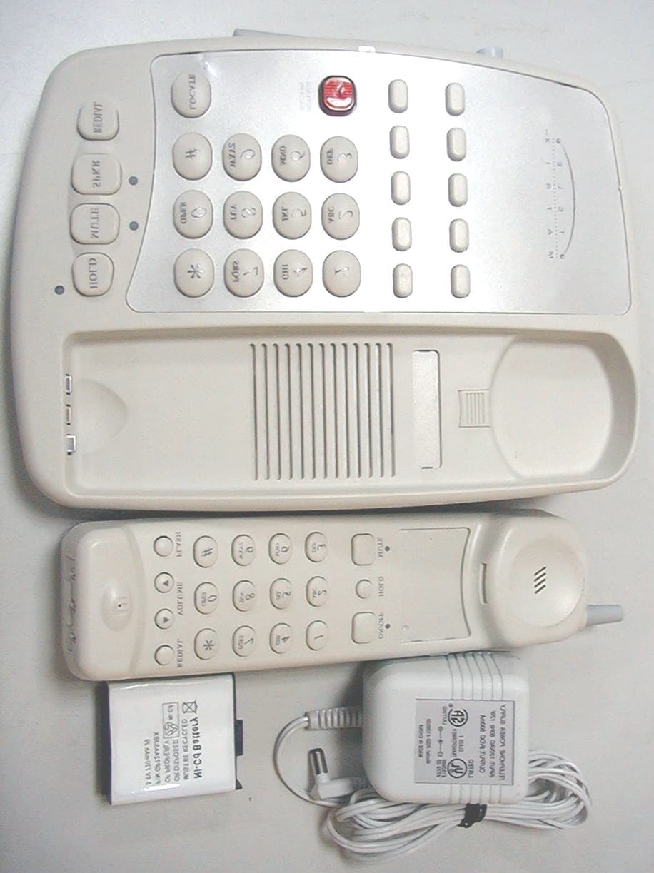
OTH-9000MWD
Jul 23, 2001Single S. S. T. Cordless Phone
Equipment Class
DSS - Part 15 Spread Spectrum Transmitter
OTH-9002MWD
Feb 21, 2000Two Line S.S.T. Cordless Phone
Equipment Class
DSS - Part 15 Spread Spectrum Transmitter