OUSCLV2TD-4Low Band VHF Digital Broadcast Transmitter
UBS-Axcera
Click to zoom
Application Details
- Equipment Class
- TBC - Licensed Broadcast Station Transmitter
- Date of Grant
- Aug 22, 2013
- Application Purpose
- Original Equipment
- Date of Application
- Aug 22, 2013
- Equipment Note
- Low Band VHF Digital Broadcast Transmitter
- Frequency Range
- 54.00000000 - 72.00000000
- Company
- UBS-Axcera
- Country
- United States
Documents & Files
Document Text
Text extracted from the exhibit documents filed with the FCC. Open a document above to read the original.
Users Manual
Instruction Manual Innovator, CLV1TD/CLV1RD (500W) to CLV4TD/CLV4RD (2000W) VHF Low Band, ATSC Transmitter/ Regenerative Translator w/Adaptive Modulator UBS-Axcera Inc. 103 Freedom Drive • P.O. Box 525 • Lawrence, PA 15055-0525, USA Phone: 724-873-8100 • Fax: 724-873-8105 www.UBS-Axcera.com • [email protected] RESTRICTIONS ON USE, DUPLICATION OR DISCLOSURE OF PROPRIETARY INFORMATION This document contains information proprietary to UBS-Axcera, to its affiliates or to a third party to which UBS-Axcera may have a legal obligation to protect such information from unauthorized disclosure, use or duplication. Any disclosure, use or duplication of this document or any of the information herein for other than the specific purpose for which it was disclosed by UBS-Axcera is expressly prohibited, except as UBS-Axcera may otherwise agree in writing. Recipient by accepting this document agrees to the above stated conditional use of this document and this information disclosed herein. Copyright © 2012, UBS-Axcera NOTE: This equipment has been tested and found to comply with the limits for a Class A digital device, pursuant to part 15 of the FCC Rules. These limits are designed to pro-vide reasonable protection against harmful interference when the equipment is operated in a commercial environment. This equipment generates, uses, and can radiate radio frequency energy and, if not installed and used in accordance with the instruction manual, may cause harmful interference to radio communications. Operation of this equipment in a residential area is likely to cause harmful interference in which case the user will be required to correct the interference at his own expense. Innovator CLV1TD/CLV1RD – CLV4TD/CLV4RD Table of Contents ATSC Transmitter/Regenerative Translator Instruction Manual, Rev. 0 i 6/17/13 Table of Contents Chapter 1 Introduction........................................................................................ 1 1.1 Manual Overview....................................................................................... 1 1.2 UBS-Axcera Numbering System Explanation.................................................. 1 1.3 Assembly Designators ................................................................................ 1 1.4 Safety ..................................................................................................... 2 1.5 Contact Information................................................................................... 3 1.6 Return Material Procedure .......................................................................... 3 1.7 Limited One Year Warranty for UBS-Axcera Products ...................................... 4 Chapter 2 System Description ............................................................................ 11 2.1 Product Architecture ................................................................................ 11 2.2 CX Drawer.............................................................................................. 11 2.3 Amplifier Drawers.................................................................................... 12 2.4 Air Cooled Assembly ................................................................................ 15 2.5 Power Supply Assembly............................................................................ 15 2.6 Optional Remote Interface with Dual Exciter Switching System ...................... 16 2.7 Pre-Filter Sample (Non-Linear Distortion).................................................... 17 2.8 Post-Filter Sample (Linear Distortion) ......................................................... 17 Chapter 3 Unpacking, Installation and Maintenance............................................... 19 3.1 Unpacking .............................................................................................. 19 3.2 Installation Overview ............................................................................... 20 3.3 CX Drawer Slide-rail Installation ................................................................ 21 3.4 Amplifier Installation and Removal ............................................................. 22 3.5 DC Power Supply Chassis Shelf and Module Installation and Removal.............. 23 3.6 AC Input Connections .............................................................................. 23 3.6.1 AC Distribution Box ........................................................................... 23 3.6.2 AC Distribution Panel ......................................................................... 24 3.6.3 Power Requirements .......................................................................... 24 3.7 Input and Output Connections................................................................... 24 3.7.1 CX Drawer........................................................................................ 24 3.7.1.1 Input Connections ....................................................................... 26 3.7.1.2 Output Connection....................................................................... 27 3.7.1.3 Power Monitoring Connections to J11 ............................................. 27 3.7.1.4 Remote Connections to J12........................................................... 28 3.7.2 Vertically Mounted HPA ...................................................................... 30 3.7.3 Optional K-Tech Receiver.................................................................... 31 3.8 Connecting your Transmitter to a TCP/IP Network ........................................ 31 3.9 Maintenance ........................................................................................... 32 Chapter 4 Initial On Site Turn On Procedure......................................................... 33 4.1 Turn On Procedure .................................................................................. 33 4.2 Typical System Operating Parameters........................................................ 3…
Text truncated - open the document above for the full version.
Cover Letter(s)
1(1) 103 Freedom Drive P.O. Box 525 Lawrence, PA 15055-0525 Attention: Application Examiner July 18, 2013 Re: Request for confidentiality Applicant: Axcera, LLC FCC ID: OUSCLV2TD To whom it may concern, Request is hereby submitted by Axcera LLC to withhold permanently from public review certain portions of the application for equipment certification for the referenced FCC identifier. This request for confidentiality is made pursuant to 47 CFR 0.457(d) and 0.459 of the FCC Rules. In particular, the following sections of the application are to be kept permanently confidential: Schematics Detailed Block diagrams Rationale for request for confidentiality: Axcera has invested considerable time and materials in research and development to produce the referenced product. Disclosure of the permanently confidential portions of this application to competitors would not only give them significant competitive advantages in developing similar products, but would also disclose successful implementation of unpublished, leading edge technology developed by us.
Internal Photos
UBS-Axcera-CLV2RD-4 FCC Equipment Authorization Report Internal Photos 8/12/2013 6-1 6. INTERNAL PHOTOS 6.1 Top view, CLV2RD Transmitter (Driver) UBS-Axcera-CLV2RD-4 FCC Equipment Authorization Report Internal Photos 8/12/2013 6-2 6.2 Top View UBS-Axcera CLV2RD Transmitter, Amplifier UBS-Axcera-CLV2RD-4 FCC Equipment Authorization Report Internal Photos 8/12/2013 6-3
Operational Description
UBS-Axcera-CLV2TD Equipment Authorization Report Operational Description 8/12/2013 8-1 8. OPERATIONAL DESCRIPTION - MODEL Axcera-CU150BTD 8.1 General Description The CLV2RD is a complete 1000-watt Low Band VHF solid-state, digital television transmitter. It operates at a nominal output power of up to 1000 watts average. 8.2 Technical Specifications Type of Emission ...................................................................... 6M00K1D Frequency Range ......................................................... 54 MHz to 88 MHz Output Power ............................................................ 1000 watts average 8.3 Performance Specifications Operating Frequency Range .......................................... 54 MHz to 88 MHz RF output - Nominal: Power ............................................................ 1000 watts average Impedance ..................................................................... 50 ohms Connector .............................................................................. “N” Regulation of Output ......................................................................... 3% Signal-to-Noise Ratio (SNR) ........................................... 30 dB or better Carrier Frequency Stability ........................................................ ±1000 Hz Data Interface: Input Rate ..................................................... 19.39 Mbps, 6 MHz Channel Input Interface .......................................................... SMPTE 310M or ASI Electrical Requirements Power Line Voltage ............................................ 208 - 240 volts, 50/60 Hz Power Consumption ............................................................... 4,600 watts Environmental Maximum Altitude ................................................................... 8,500 feet Operational Temperature Range ........................................... 0C to +50C UBS-Axcera-CLV2TD Equipment Authorization Report Operational Description 8/12/2013 8-2 Mechanical Dimensions: Width .................................................................................... 22” Height ................................................................................... 76” Depth ................................................................................... 34” Weight .......................................................................... 650 lbs 8.4. System Overview The CHV4TD is made up of the trays/assemblies listed in Table 8-1. Table 8-1. HLV2RD Major Trays and Assemblies MAJOR ASSEMBLY DESIGNATOR TRAY/ASSEMBLY NAME A1 Digital Transmitter (Driver) A2 Amplifier A3 Amplifier 8.4.1 Digital Modulator The modulator accepts an ASTC transport stream in SMPTE 310 or ASI Format input and outputs an 8-VSB RF signal at the desired center frequency. The signal generation function of the modulator is also referred to as the “forward signal path” in this manual. There is also a “reverse signal path” that is used for automatic adaptive equalization. Two transmitter output samples are taken from directional couplers located before and after the channel mask filter and are applied to modulator or the external relay. The modulator contains a down-converter that converts the RF sample to a digital sample. The down-converted sample is digitized by the modulator. It is then demodulated in non-real time software. The result is analyzed to calculate linear and nonlinear adaptive equalizers to improve the transmitted signal quality by compensating for the nonlinear compression of the power amplifier and the linear distortions (mostly group delay effects) of the channel filter. When a linear adaptive equalizer is being calculated the transmitter sample is taken after the channel mask filter so that its linear distortions can be “seen.” When a nonlinear adaptive equalizer is being calculated the transmitter sample is taken before the channel mask filter so that the distortion sidebands being generated by the power amplifier can be seen (the channel filter would remove the out-of-band sidebands). The modulator contains an embedded computer. The computer performs user interface functions and the numerical processing necessary for the adaptive linear and nonlinear equalization. 8.4.2 Digital Transmitter (Driver) The Transmitter Driver provides an On Channel output signal and is used as the pre-driver for the external amplifiers. UBS-Axcera-CLV2TD Equipment Authorization Report Operational Description 8/12/2013 8-3 8.4.2.1 (A5) ALC Board (1315006) The ALC Board of the Innovator CX is used to control the RF drive power to the RF amplifier chain in the HLV2RD. The board accepts a digital RF input signal at a nominal input level of -3 dBm average power and amplifies it to whatever drive level is necessary to drive the final RF amplifier in the tray to full power. The input signal to the board at J1 is split by U4, with one half of the signal driving a PIN diode attenuator, DS1 and DS2, and the other half driving a detector, U13, that is used to mute the PIN attenuator when there is no input signal. The output of the PIN attenuator is sent to two cascaded amplifiers, U2 and U3, which are capable of generating +10 dBm average power from the board at J2. The PIN attenuator is driven by an ALC circuit or by a manual fixed voltage bias, depending on the position of switch S1. When the switch is pointing to the left, looking from the front of the tray, the ALC circuit is enabled. When the switch is pointing to the right, the ALC circuit is disabled and the PIN attenuator is controlled through the Manual gain pot R62. When the switch is in either ALC or manual, the voltage in the unused circuit is preset low by the circuitry connected to pins 4-6 on SW1. This allows the RF power to ramp up slowly to full power when the switch changes positions. CR8, C33 and associated components control the ramp up speed of the manual gain circuit. CR9, C42 and their associated circuits do the same thing for the ALC circui…
Text truncated - open the document above for the full version.
Operational Description
Innovator CBX Firmware Features 1316306: CODE, CXB, PTV ATSC MOD K:\METrak_Job_Folders\2013\U\UBS-Axcera, Inc - UBS\39431\TCB\Customer Info\Innovator CLV Modulator 1316306 Features.doc Background The Innovator CXB has a set of menus that allow an operator to view read only parameters and another set to configure parameters of the transmitter. This document describes the menus added to implement the ProTV ATSC modulator within the CXB. Axcera part number 1316306 is assigned to the system controller software package that implements these screens. 1616307 is assigned to the ethernet controller code used with this system controller code to access web pages of the ProTV ATSC modulator. Implementation 1. Section 2. Menus 2.1. Splash Screens Figure 2.1-1: Software Splash Screen P/N: 1316306 firmware version level 2.0b and EPLD version 2.5 2.2. Device Details Screens These are read only parameters. 2.2.1. Device Details Screens - ATSC Modulator Figure 2.2.1-1: Device Details - ATSC Modulator Select Menu Level ATSC Details Top Level Description This screen provides access to the read only parameters of the ATSC modulator. Parameter Range N/A 2.2.1.1. Device Details - ATSC Modulator - Input Signals Innovator CBX Firmware Features 1316306: CODE, CXB, PTV ATSC MOD K:\METrak_Job_Folders\2013\U\UBS-Axcera, Inc - UBS\39431\TCB\Customer Info\Innovator CLV Modulator 1316306 Features.doc Figure 2.2.1.1-1: Device Details - Input Signals Catagory Menu Level ATSC Details / Input Signals Top Level Description This screen provides access to read only input signal parameters of the ATSC modulator. Parameter Range N/A Figure 2.2.1.1-2: Device Details - Input Signals - Selected Stream Menu Level ATSC Details / Input Signals / Selected Stream Description This screen indicated which input path is currently selected. Parameter Range Input #1 or Input #2 Figure 2.2.1.1-3: Device Details - Input Signals - Primary Stream Status Menu Level ATSC Details / Input Signals / Primary Stream Description This menu indicates if the allocated primary stream is available or not. Parameter Range "Available" or "No Sync Signal" Figure 2.2.1.1-4: Device Details - Input Signals - Secondary Stream Status Menu Level ATSC Details / Input Signals / Secondary Stream Description This menu indicates if the secondary stream is available or not. Parameter Range "Available" or "No Sync Signal" Figure 2.2.1.1-5: Device Details - Input Signals - Primary Stream: Number of Buffered Packets Menu Level ATSC Details / Input Signals / Primary Buffered Packet Count Description This display indicates how many packets are stored in the input buffer. Parameter Range Minimum of 0 Figure 2.2.1.1-6: Device Details - Input Signals - Primary Stream: Packet Size Menu Level ATSC Details / Input Signals / Primary Stream Packet Size Description This display indicates the primary transport stream packet size. Parameter Range 188 or 204 Innovator CBX Firmware Features 1316306: CODE, CXB, PTV ATSC MOD K:\METrak_Job_Folders\2013\U\UBS-Axcera, Inc - UBS\39431\TCB\Customer Info\Innovator CLV Modulator 1316306 Features.doc Figure 2.2.1.1-7: Device Details - Input Signals - Primary Stream: Bit Rate Menu Level ATSC Details / Input Signals / Primary Stream Bit Rate Description This is the detected bit rate of the primary input transport stream. Parameter Range Figure 2.2.1.1-8: Device Details - Input Signals - Primary Stream: Stuffing Rate Menu Level ATSC Details / Input Signals / Primary Stream Stuffing Rate Description This is the detected stuffing rate of the primary input transport stream. Parameter Range Figure 2.2.1.1-9: Device Details - Input Signals - Primary Stream: TS ID Menu Level ATSC Details / Input Signals / Primary Stream TS ID Value Description This is the detected TS ID value of the primary input stream. Parameter Range 0 to 65535 2.2.1.2. Device Details - ATSC Modulator - Adaptive Status Figure 2.2.1.2-1: Device Details - Adaptive Precorrection Status Catagory Menu Level ATSC Details / Adaptive Status Top Level Description This screen provides access to read only adaptive system parameters. Parameter Range N/A Figure 2.2.1.2-2: Device Details - Adaptive Signals - Lower Shoulder Level Menu Level ATSC Details / Adaptive Signals / Lower Shoulder Value Description When valid, this is the measured level in dB for the lower shoulder. Parameter Range 'Invalid' or measured level in dB Innovator CBX Firmware Features 1316306: CODE, CXB, PTV ATSC MOD K:\METrak_Job_Folders\2013\U\UBS-Axcera, Inc - UBS\39431\TCB\Customer Info\Innovator CLV Modulator 1316306 Features.doc Figure 2.2.1.2-3: Device Details - Adaptive Signals - Upper Shoulder Level Menu Level ATSC Details / Adaptive Signals / Upper Shoulder Value Description When valid, this is the measured level in dB for the upper shoulder. Parameter Range 'Invalid' or measured level in dB Figure 2.2.1.2-4: Device Details - Adaptive Signals - Amplitude Ripple Menu Level ATSC Details / Adaptive Signals / Amplitude Ripple Value Description When valid, this is the measured level in dB for the amplitude ripple. Parameter Range 'Invalid' or measured level in dB. Figure 2.2.1.2-5: Device Details - Adaptive Signals - Group Delay Menu Level ATSC Details / Adaptive Signals / Group Delay Value Description When valid, this is the measured group delay in nano seconds. Parameter Range 'Invalid' or measured level in nS. Figure 2.2.1.2-6: Device Details - Adaptive Signals - Nonlinear Sample Menu Level ATSC Details / Adaptive Signals / Nonlinear Sample Level Description When valid, this is the RF sample level used for nonlinear precorrection. Parameter Range 'Invalid' or measured level in dB. Required level for precorrection is 0 dBm +/- 10 dB. Figure 2.2.1.2-7: Device Details - Adaptive Signals - Nonlinear Correction Operational Mode Menu Level ATSC Details / Adaptive Signals / Nonlinear Adjust Mode Description Nonlinear Precorrection can be enabled or disabled through read / write parameters. This value tells us the operational status …
Text truncated - open the document above for the full version.
Parts List/Tune Up Info
UBS-Axcera-CLV2TD-4 FCC Equipment Authorization Report Parts List/Tune- up Info 8/12/2013 7-1 7. PARTS LIST/TUNE-UP INFO 7.1 Parts List The transmitter, can be subdivided as follows: Modulator – RF output ALC Board Output Detector Board Control Card Board Astec multi-voltage supply 35W Amplifier Board Two Stage VHF Amplifier Board Switching Power Supply Amplifier Control board Splitter / Combiner Output metering board System metering board Combiner Mask Filter 7.2 Tune-Up Information This transmitter was aligned at the factory and should not require additional adjustments to achieve normal operation. This transmitter is of a tray design with multiple boards inside the tray. If a board fails, that board needs to be changed out with a replacement board. The failed board can then be sent back for repair. 7.2.1 Set-Up of the Output Power of the Transmitter Check that the Auto/Man switch S1 on the ALC Board is in the Automatic ALC position. Adjust R75 the ALC pot on the ALC Board as needed to attain 100% output power. Switch to Manual Gain (Manual ALC) and adjust the Manual Gain pot R62 for 100 % output power. Switch the ALC Board back to Automatic ALC. 7.2.2 ALC Board Set-Up in the Tray On (A5) the ALC Board (1315006), preset the Overdrive Threshold pot R38 full CW and set R62, Manual Adjust, and R75, ALC Adjust, full CCW. Apply an 8-VSB signal at -3 dBm average level to the J1 input jack to the tray. Switch S1 to Manual Gain, and increase the output power to 100%. Calibrate the transmitter output power using R23, Forward Calibration pot, on the Output Detector Board. Turn the output power down to 10% power. Remove the output RF connector from J2 on tray and calibrate the reflected power to 10%, using R7, the Reflected Calibration pot, on the Output Detector Board. Re-connect the RF output connector to the tray and increase the power, in Manual gain, to 125%. Adjust the Overdrive pot R38, CCW until the overdrive threshold just trips and the Overdrive Fault LED DS4 lights. Turn the pot slightly CW so that power comes back up and DS4 goes out. Switch S1 to ALC. Turn the ALC Adjust pot R75 until the power is 100%. Switch S1 UBS-Axcera-CLV2TD-4 FCC Equipment Authorization Report Parts List/Tune- up Info 8/12/2013 7-2 between ALC and Manual to verify smooth switching, with minimal change in power. Switch the tray Off and insert a 10 dB attenuator at the input. Switch the tray On and verify the input fault LED comes on and the RF power Mutes. Output power should drop by at least 20-30 dB. Switch the tray Off and remove the 10 dB attenuator. Replace the input connector and turn the tray back on. With the tray in ALC, use the ALC Adjust pot, R75, to decrease the power to 10%. Remove the RF output connector from the tray. Verify that the VSWR Cutback LED, DS6, comes on and the Reflected Power drops to approximately 6%. Reconnect the RF output connector and increase the power back up to 100%. This completes the set up of the ALC board. 6 MHz -35 dB -110 dB 3 MHz 6 MHz Figure 3: Typical Digital Spectrum 7.2.3 Linearity Correction Adjustment (Non-Linear Distortions) As shipped, the transmitter was preset to include amplitude and phase pre-distortion. The pre-distortion was adjusted to approximately compensate the corresponding non-linear distortions of the Power Amplifier. All adjustments are made using the Modulator. The transmitter is now set up and ready for normal operation.
Test Report
UBS-Axcera – HLV2RD Equipment Authorization Report – Part 74 Test Report JULY 2013 4-1 4. TEST REPORT 4.1 RF Power Measurements Figure 4-1 shows the test equipment setup for the RF power measurements. Figure 4-1. Test Equipment Setup for RF Power Measurements The output power of the HLV2RD was adjusted to obtain 1000 watts average RF output as observed on the power meter. Per FCC 2.1046. Measured Power: +10 dBm Coupling Loss: -50.0 dB Power: +60 dBm Power = 1000 Watts With the power level properly set to 1000 watts average, all required tests were performed and recorded in the following sections. HLV2RD-5 Transmitter Hewlett Packard Power Meter Bird Model 8890-300 50 Ohm Termination Connecticut Microwave Directional Coupler RFA-300 Test Measurement Set & EFA 2067.3004.53 8VSB Demodulator HP Spectrum Analyzer Device Under Test Bandpass Filter Directional Coupler UBS-Axcera – HLV2RD Equipment Authorization Report – Part 74 Test Report JULY 2013 4-2 4. 2 Modulation Characteristics The modulator tray incorporates a modulation technique known as 8-Level Vestigial Side-band (8-VSB), which uses a layered digital architecture and a single carrier frequency. A pilot tone is provided, to allow rapid acquisition of the signal by receivers. The 8-VSB system transmits a serial data bit stream at a rate of 19.4 Mbps in a 6 MHz television channel. This type of transmission is far less susceptible to propagation impairments such as multi-path, noise and interference as compared to analog transmissions. The modulator is fully adaptive to correct linear and nonlinear distortions. Per FCC 2.1047. Figure 4-2. Typical Demodulation Test Setup HLV2RD Transmitter Directional Coupler 50 Ohm Termination 20 dB Attenuator Device Under Test EFA 2067.3004.53 8VSB Demodulator Bandpass Filter Directional Coupler RFA-300 Test Measurement Set UBS-Axcera – HLV2RD Equipment Authorization Report – Part 74 Test Report JULY 2013 4-3 4. 3 Error Vector Magnitude (EVM) and Signal to Noise Ratio (SNR) The Rohde & Schwarz EFA Signal Analyzer was used to measure that the un-equalized patterns are within the ATSC/FCC EVM limit of 4% and SNR limit of 27db. Figure 4-3. SNR Measurement UBS-Axcera – HLV2RD Equipment Authorization Report – Part 74 Test Report JULY 2013 4-4 4. 4 Frequency Response Figure 4-4. Frequency Response Plot UBS-Axcera – HLV2RD Equipment Authorization Report – Part 74 Test Report JULY 2013 4-5 4. 5 Peak to Average Figure 4-5. Peak to Average Plot UBS-Axcera – HLV2RD Equipment Authorization Report – Part 74 Test Report JULY 2013 4-6 4. 6 Phase Noise Figure 4-6. Phase Noise Plot UBS-Axcera – HLV2RD Equipment Authorization Report – Part 74 Test Report JULY 2013 4-7 4.7 Occupied Bandwidth Using the test setup in Figure 4-2, with the transmitter operating at maximum power, a photograph of the transmitter occupied bandwidth spectrum was taken and is shown in Figure 4-7. Per FCC 2.1049 Figure 4-7. Channel Occupied Bandwidth 1000W (Post-Filter) UBS-Axcera – HLV2RD Equipment Authorization Report – Part 74 Test Report JULY 2013 4-8 Occupied Bandwidth 20dB points UBS-Axcera – HLV2RD Equipment Authorization Report – Part 74 Test Report JULY 2013 4-9 Occupied Bandwidth 26dB points UBS-Axcera – HLV2RD Equipment Authorization Report – Part 74 Test Report JULY 2013 4-10 4.8 Conducted Spurious Emissions The Hewlett Packard Spectrum Analyzer was used to measure harmonics before mask filter. The levels were then added to the filter attenuation at the 2 nd and 3 rd harmonics for a reading of less than -76dB at the output of the mask filter. Figure 4-8A. Reference (69.00 MHz) = 0dBc (Pre-Filter) UBS-Axcera – HLV2RD Equipment Authorization Report – Part 74 Test Report JULY 2013 4-11 Figure 4-8B. Second Harmonic (1174.00 MHz) = -15 dBc(Pre-Filter) UBS-Axcera – HLV2RD Equipment Authorization Report – Part 74 Test Report JULY 2013 4-12 Figure 4-8C. Third Harmonic (1761.00 MHz) = <-53 dBc (Pre-Filter) UBS-Axcera – HLV2RD Equipment Authorization Report – Part 74 Test Report JULY 2013 4-13 Figure 4-8D. Bandpass Filter response UBS-Axcera – HLV2RD Equipment Authorization Report – Part 74 Test Report JULY 2013 4-14 Figure 4-8E. Bandpass Filter Harmonic response UBS-Axcera – HLV2RD Equipment Authorization Report – Part 74 Test Report JULY 2013 4-15 Figure 4-8F. Bandpass Filter response Harmonic (MHz) Level Relative to fundamental Filter Response (dB) Bandwidth correction (dB) Total (dB) Fundamental (69) ref ref --- ref Second (138) -55 -75 10.3 -140.3 Third (207) -42 -54 10.3 -106.3 Table 4-1. Post Filter Harmonic Levels The FCC rules require the energy to be measured in 500 kHz, and compared to the total channel power. The channel power is spread out evenly over an occupied bandwidth of 5.4 MHz. The total channel power is 10*log(5.4/0.5)=10.3 dB Frequency Relative Level (dBm) FCC Requirement (dBm) Fundamental 0 dB (reference) --- Second Harmonic -140.3 -76 Third Harmonic -106.3 --76 UBS-Axcera – HLV2RD Equipment Authorization Report – Part 74 Test Report JULY 2013 4-16 Part 74.794 of the Rules states: (ii) Stringent mask. In the first 500kHz from the channel edges, emissions must be attenuated no less than 47 dB. More than 3 MHz from the channel edges, emissions must be attenuated no less than 76 dB. At any frequency between 0.5 and 3 MHz from the channel edges, emissions must be attenuated no less than the value determined by the following formula: A(dB) = 47 + 11.5 (Df-0.5 (i) Simple mask. At the channel edges, emissions must be attenuated no less than 46 dB. More than 6 MHz from the channel edges, emissions must be attenuated no less than 71 dB. At any frequency between 0 and 6 MHz from the channel edges, emissions must be attenuated no less than the value determined by the following formula: A (dB) = 46 + (Δf 2 /1.44) Figure 4-8J. Out of Band Emissions (Post Filter) UBS-Axcera – HLV2RD Equipment Authorization Report – Part 74 Test Report JULY 2013 4-17 100W Post Filter UBS-Axcera – HLV2RD Equipment Authorization Report – Part 74 Test Repor…
Text truncated - open the document above for the full version.
Test Report
UBS-Axcera CLV2TD-4 FCC Equipment Authorization Report Certification of Test Data 8/12/2013 9-1 9. CERTIFICATION OF TEST DATA This equipment has been tested in accordance with the requirements contained in the appropriate Commission regulation. To the best of my knowledge, these tests were performed using measurement procedures consistent with the industry or Commission standards and demonstrate that the equipment complies with the appropriate standards. Each unit manufactured, imported or marketed, as defined in the Commission's regulations, will conform to the sample(s) tested within the variations that can be expected due to quantity production and testing on a statistical basis. I further certify that the necessary measurements were made by Axcera, LLC, 103 Freedom Drive, P.O. Box 525, Lawrence, PA 15055-0525
Contact Information
Applicant
David Hewitt(Engineering Manager)
Technical Contact
UBS-Axcera IncTom Botwright
[email protected]724-873-8100
103 Freedom Drive · Lawrence, Pennsylvania · United States
Technical Specifications
| # | Rule Parts | Frequency Range | Power Output | Emission | Tolerance |
|---|---|---|---|---|---|
| 2 | 74 | 54 MHz - 72 MHz | 100 W | 5M59K1D | 1000 Hz |
Other Applications from UBS-Axcera

OUSCU0TD-5-UBS
Mar 27, 2014200W UHF Digital Transmitter
Equipment Class
TBC - Licensed Broadcast Station Transmitter
OUSCL1TC-4
Sep 17, 2013400-Watt, 1.6 GHz DVB-H Transmitter
Equipment Class
TNB - Licensed Non-Broadcast Station Transmitter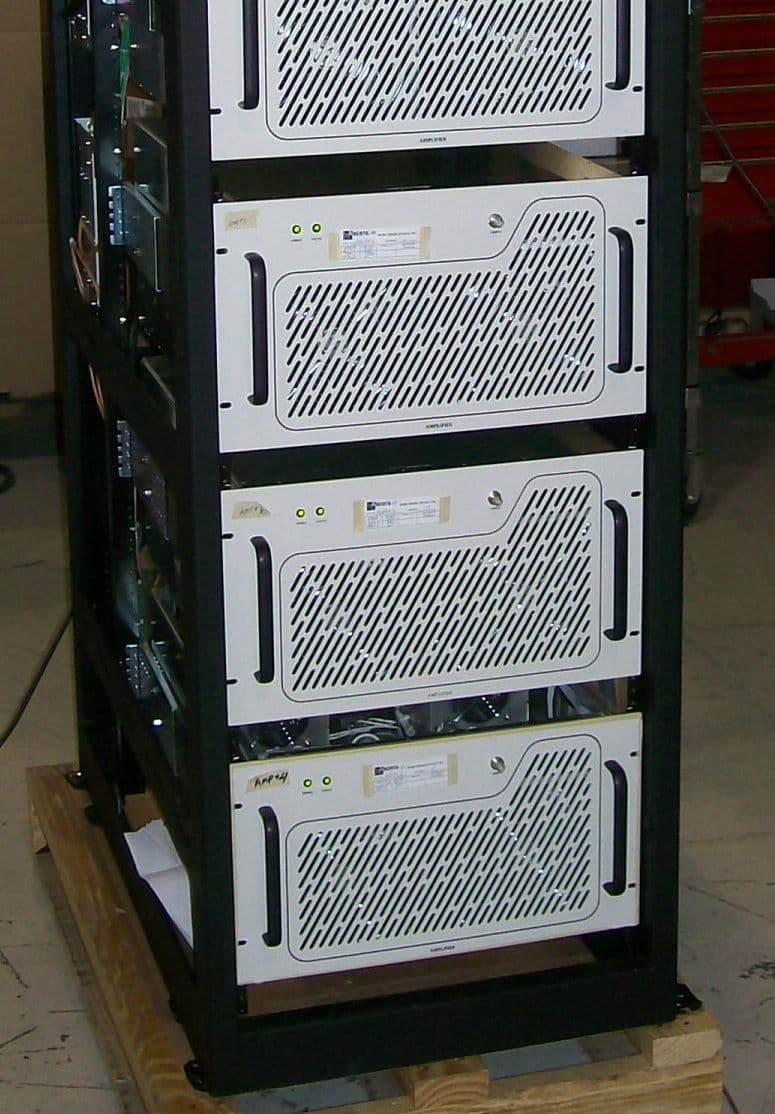
OUSCHV4TD
Jun 14, 20123000-Watt VHF Digital Transmitter
Equipment Class
TBC - Licensed Broadcast Station Transmitter
OUSCU0TD-5
Dec 14, 2011200 Watt UHF Digital Transmitter
Equipment Class
TBC - Licensed Broadcast Station Transmitter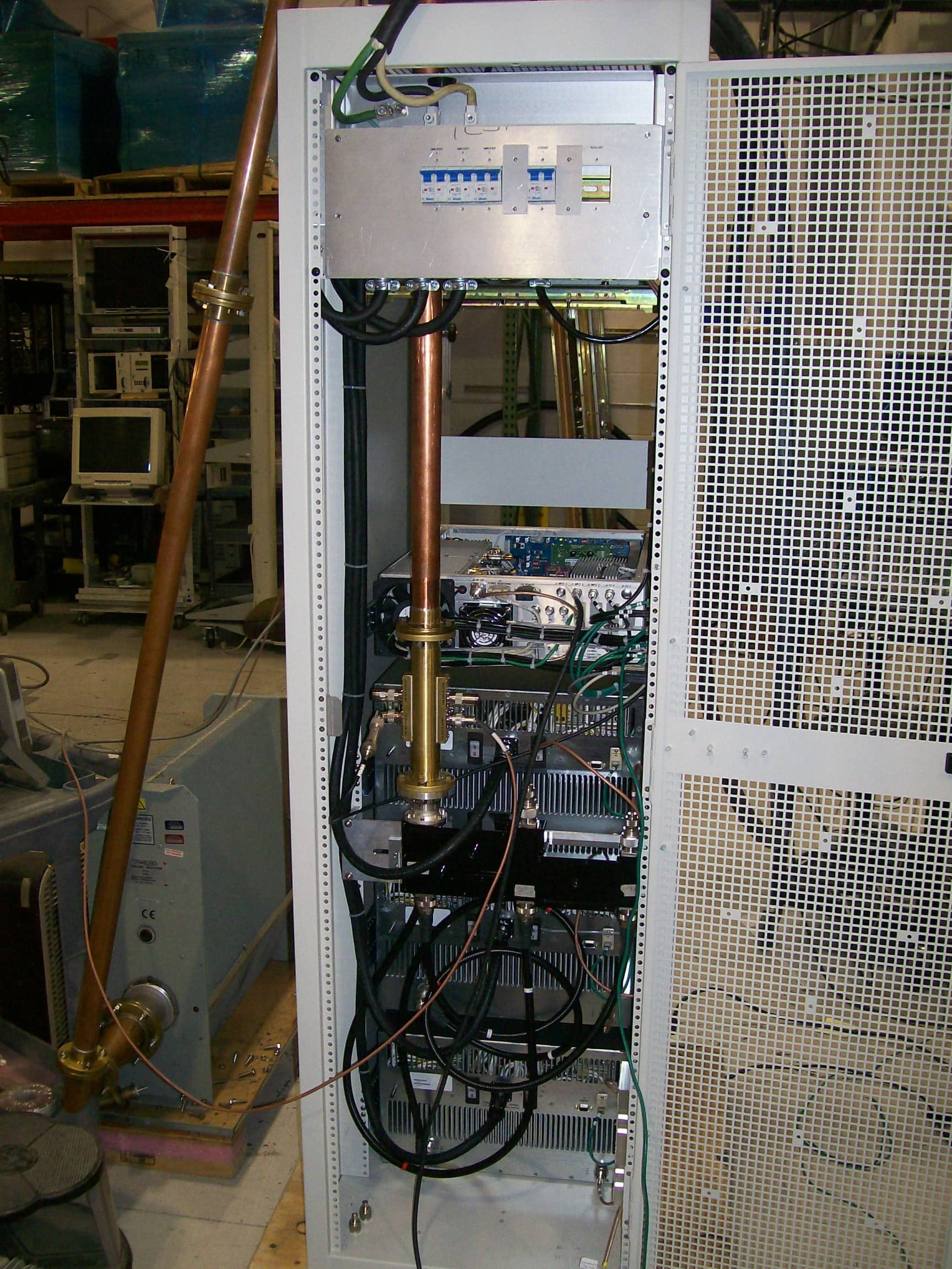
OUSCU3TD
Dec 14, 20112500 Watt UHF Digital Transmitter
Equipment Class
TBC - Licensed Broadcast Station Transmitter