FCCID.CO- FCC ID Database
HomeCompaniesEquipment ClassesSearch

© 2026 FCC ID Database. All rights reserved.

AboutContactData sourced from FCC public records
  1. Home/
  2. Comuniq Inc./
  3. OXLPCI-PMC

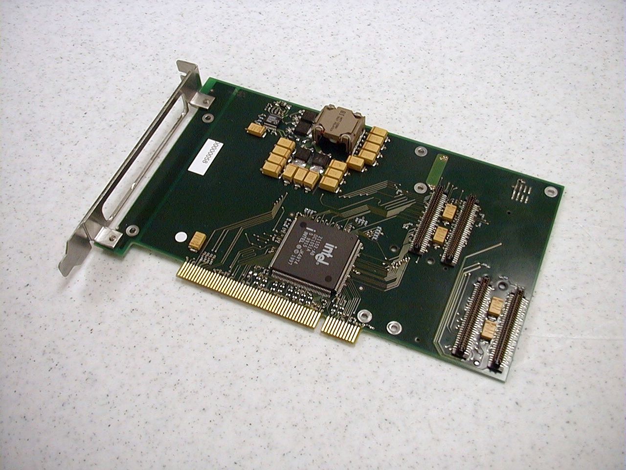
OXLPCI-PMCPCI-to-PMC Carrier Card

Comuniq Inc.
PCI-to-PMC Carrier Card - FCC ID OXLPCI-PMC - Comuniq Inc.
Click to zoom

Application Details

Equipment Class
JBP - Part 15 Class B Computing Device Peripheral
Date of Grant
Mar 24, 2000
Application Purpose
Original Equipment
Date of Application
Mar 15, 2000
Equipment Note
PCI-to-PMC Carrier Card
Frequency Range
33.00000000 - 33.00000000
Company
Comuniq Inc.
Country
United States

Documents & Files

Select a file to view

Users Manual

↗

Block Diagram

↗

External Photos

↗
↗

ID Label/Location Info

↗

Operational Description

↗

Schematics

↗
↗

Test Setup Photos

↗

Document Text

Text extracted from the exhibit documents filed with the FCC. Open a document above to read the original.

Users Manual

SMAS E1/T1 BOARD User Guide Comuniq ASA Version 2.0 – March 2000 Comuniq ASA SMAS User Guide 2.0 Page 2 of 9 Statement of compliance This device complies with part 15 of the FCC rules. Operation is subject to the following two conditions: (1) This device may not cause harmful interference, and (2) this device must accept any interference received, including interference that may cause undesired operation. NOTICE The information in this publication is subject to change without notice. This document contains proprietary information disclosed under a non-disclosure agreement. Disclosure to any third party without written permission from Comuniq ASA is in violation of the non-disclosure agreement. COMUNIQ ASA SHALL NOT BE HELD LIABLE FOR TECHNICAL OR EDITORIAL ERRORS OR OMISSIONS CONTAINED HEREIN, NOR FOR INCIDENTAL OR CONSEQUENTIAL DAMAGES RESULTING FROM THE FURNISHING, PERFORMANCE, OR USE OF THIS MATERIA L. This publication contains information protected by copyright. No part of this publication may be reproduced or utilized in any form or by any means, electronic or mechanical, including photocopying and microfilm, without written permission from Comuniq ASA. Product names mentioned herein may be trademarks and/or registered trademarks of their respective companies. © 2000 Comuniq ASA, All rights reserved. Comuniq ASA SMAS User Guide 2.0 Page 3 of 9 Corporate HQCustomer Support Comuniq ASAComuniq Inc. Solakrossen 112046 Samco Rd. N-4050 SolaRapid City, SD 57701 NorwayUSA Phone: +47 51 71 55 55Phone: 1-605-388-3251 Fax: +47 51 71 55 56Fax: 1-605-348-4030 WEB: http://www.comuniq.comE-Mail: [email protected] Comuniq ASA SMAS User Guide 2.0 Page 4 of 9 Table of Contents CHAPTER 1..................................................................................................... INTRODUCTION 5 CHAPTER 2...................................................................................................... INSTALLATION 6 2.1H ARDW ARE ..................................................................................................................... 6 2.2S OFTWARE ...................................................................................................................... 8 2.3U PDATING THE FIRMWARE ON THE SMAS BOARD .............................................................. 9 Comuniq ASA SMAS User Guide 2.0 Page 5 of 9 Chapter 1 Introduction Comuniq’s Streaming Media Application Server (SMAS) E1/T1 resource board provides a powerful and flexible IP telecom platform for a variety of telecom functions. These include: interactive voice response, voice over IP, and unified messaging system applications. Powerful on-board CPU/DSP resources handle up to 60 channels of voice traffic, and allow extensive IP signal processing using a single PCI slot. The boards are 100% compliant with PMC specifications and fit both PCI and cPCI systems. The SMAS board draws a maximum power-load of 7.1319 volts +/- 5% and an average power load of 6.0672 volts. This hardware is supported by an integrated software suite that offers easy access to all of the SMAS board’s functio ns using Wi ndo ws NT, Solaris, or Li nu x. The open Application Progra mmer ’s Interface (API) and extensible message interface facilitates efficient development and integration of third party software. Using the SMAS API, a programmer working with visual studio can develop a simple voice mail system with remarkably little code. Developers using the Microsoft COM environment can also access the board’s functionality using the SMAS COM object or ActiveX control. This document explains the installation and use of the E1/T1 interface board and software. The target system for the SMAS board must comply with the following requirements: ProcessorPentium 200MHz, minimum HD space100 MB of available hard-disk space, minimum Memo ry64 MB, mi ni mu m 128 MB, recommended when running more than 30 channels of IVR DisplayVGA, 800 x 600, 256-color video adapter Operating SystemWindows NT 4.0 (service pack 3 or later) Development EnvironmentVisual Studio with service pack 3 or later MotherboardPCI ver 2.1 or later, 32 bit @ 33 MHz Comuniq ASA SMAS User Guide 2.0 Page 6 of 9 Chapter 2 Installation 2.1 Hardware 2.1.1 Safety Notes Before installation, please observe the following: WARNING! Turn the computer off, disconnect the power source, and allow the internal components to cool before beginning installation. This will reduce the risk of personal injury from hot surfaces and electrical hazards . The SMAS board is a static sensitive device and requires compliance with static precaution measures. CAUTION: Electrostatic discharge can damage electronic components. Be sure you are properly grounded before beginning this procedure. Proper packaging and grounding techniques are necessary precautions to prevent damage. To prevent electrostatic damage observe the following precautions: • Transport products in static-safe containers such as conductive tubes, bags, or boxes. • Keep electrostatic-sensitive parts in their containers until they arrive at static-free stations. • Cover work areas with an approved static-dissipating material. Wear a grounding wrist strap that has been connected to the work surface, and make sure that all tools and equipment are properly grounded. • Keep work area free of non-conductive materials including the plastic assembly aids and foam used in packing. • Always wear a properly grounded wrist strap when touching a static-sensitive component or assembly. • Avoid touching pins, leads, or circuitry. 2.1.2 Installation Before beginning installation, turn off all power to the computer designated for the installation of the SMAS board. Failure to do so may damage the computer and/or SMAS board. Insert the SMAS board into an available PCI or Compact PCI slot. Ensure that the board is securely held in place by either screws or clips. Comuniq ASA SMAS User Guide 2.0 Page 7 of 9 Figure 2-1 This photograph shows the SMAS board installed i…

Text truncated - open the document above for the full version.

Block Diagram

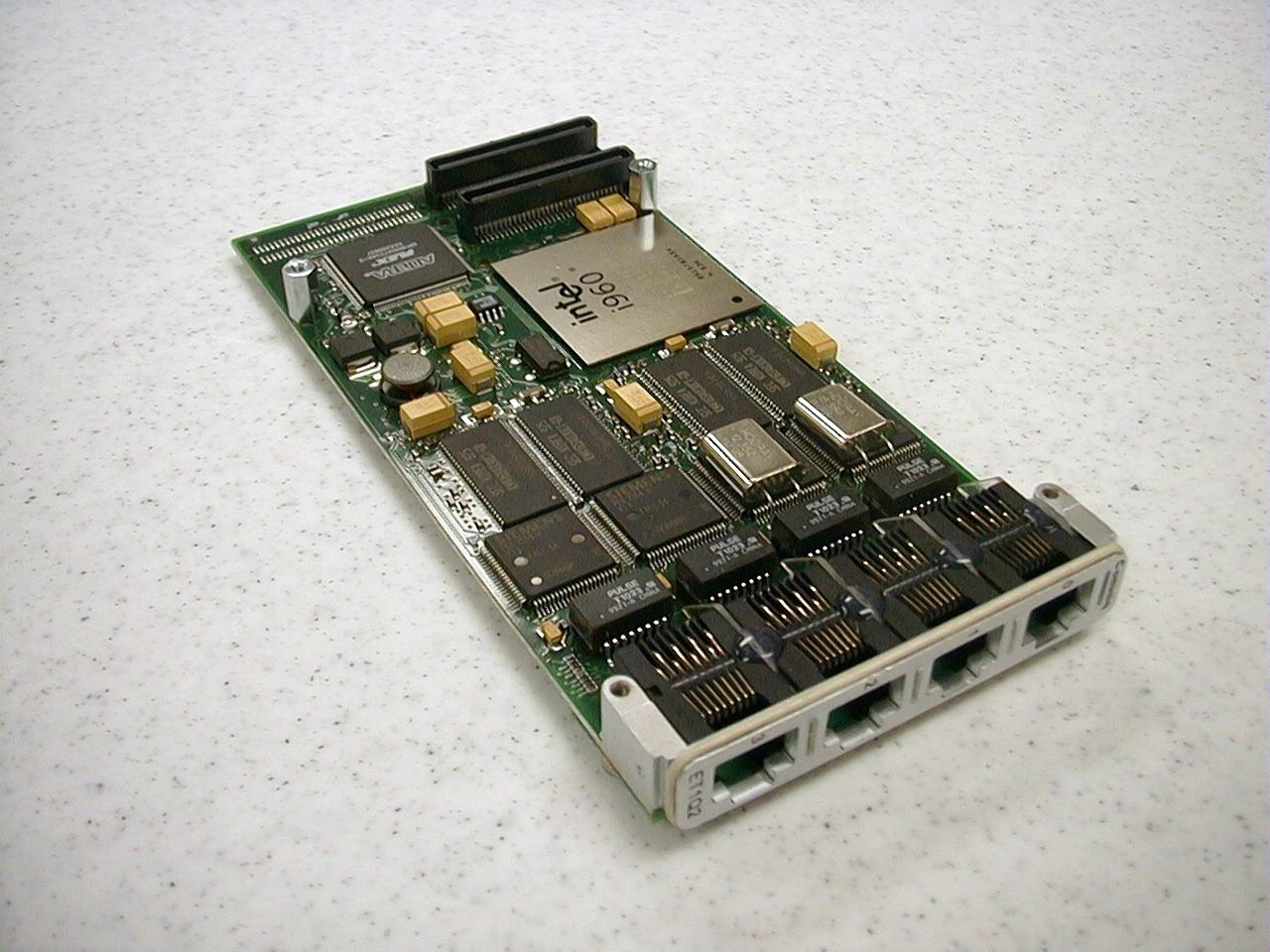
SMAS E1/T1 BOARD Block Diagram Comuniq ASA Version 2.0 – March 2000 Comuniq ASA SMAS User Guide 2.0 Page 2 of 5 NOTICE The information in this publication is subject to change without notice. This document contains proprietary information disclosed under a non-disclosure agreement. Disclosure to any third party without written permission from Comuniq ASA is in violation of the non-disclosure agreement. COMUNIQ ASA SHALL NOT BE HELD LIABLE FOR TECHNICAL OR EDITORIAL ERRORS OR OMISSIONS CONTAINED HEREIN, NOR FOR INCIDENTAL OR CONSEQUENTIAL DAMAGES RESULTING FROM THE FURNISHING, PERFORMANCE, OR USE OF THIS MATERIA L. This publication contains information protected by copyright. No part of this publication may be reproduced or utilized in any form or by any means, electronic or mechanical, including photocopying and microfilm, without written permission from Comuniq ASA. Product names mentioned herein may be trademarks and/or registered trademarks of their respective companies. © 2000 Comuniq ASA, All rights reserved. Corporate HQCustomer Support Comuniq ASAComuniq Inc. Solakrossen 112046 Samco Rd. N-4050 SolaRapid City, SD 57701 NorwayUSA Phone: +47 51 71 55 55Phone: 1-605-388-3251 Fax: +47 51 71 55 56Fax: 1-605-348-4030 WEB: http://www.comuniq.comE-Mail: [email protected] Comuniq ASA SMAS User Guide 2.0 Page 3 of 5 This document will give the reader an understanding of the functionality of the SMAS. The first section describes the system, followed by a functional description of the SMAS board. 1.1 The SMAS System SMAS is a firmware platform that enables system integrators to implement services such as Automatic Call Distribution (ACD), Interactive Voice Response (IVR), Private Branch Exchange (PBX), and IP- telephony for E1/T1 connections. The SMAS system is a scalable telephony system, which may consist of a maximum of 36 SMAS cards per Compact PCI PC. The main host of the system is a Windows NT server. The block diagram in Figure 1 illustrates the scalability where a large number SMAS cards can be attached on the PCI bus under supervision of Windows NT or a user defined host. Figure 1 – A block diagram of the SMAS telephony system. The system utilizes the PCI bus to transfer telecommunication data in a maximum configuration of 4320 voice channels for E1 and 3456 voice channels for T1. 1.2 Hardware The hardware is divided into four layers. Of these four layers, all but the host computer are physically located on the SMAS card. - Host computer, Windows NT (NT) - Embedded I 2 O Processor, Intel 80960RD (i960) - Digital Signal Processor, Texas Instrument’s TMS320C6201 (C6) - Line Interface Adapter, Siemens Falc’54 (FALC’54) The architecture enables a total of 120 full duplex voice channels per card for an E1 interface and a total of 92 (or 96) full duplex voice channels per card for a T1 interface. The E1 has, in addition, four D-channels and four synchronization channels, and T1 may have four D-channels when it is configured for use with 92 voice channels. For E1 the line interface runs at 2.048 Mbps, and for the T1 line interface runs at 1.544 Mbps. The data format on the E1/T1 side is G.711, which is standard A-Law (Europe) or μ-Law (USA and Japan). Figure 2 show the SMAS card architecture, which consists of three main components: Falc’54, C6 and i960. Windows NT I960Rx TI C62xTI C62x FALCFALCFALCFALC E1/T1 E1/T1 E1/T1 E1/T1 I960Rx TI C62xTI C62x FALCFALCFALCFALC E1/T1 E1/T1 E1/T1 E1/T1 I960Rx TI C62xTI C62x FALCFALCFALCFALC E1/T1 E1/T1 E1/T1 E1/T1 SMAS #1SMAS #2SMAS #N E1/T1E1/T1E1/T1E1/T1 SMAS #N-1 PCI/I20 Comuniq ASA SMAS User Guide 2.0 Page 4 of 5 Figure 2 also shows the memory configuration and the data flow throughout the system. The PCI interface is 32 bits and runs at 33 MHz, and it interfaces with the i960, which also runs at 33 MHz. The C6 has a 50 MHz external clock allowing 200 MHz internal operation. The Flash contains the IxWorks operating system for the i960 and the firmware code for the Altera, not illustrated in Figure 2. Downloading the program code directly from an NT application configures the system. The i960 has 16 Mbytes external DRAM memory to store data and programs. The i960 runs at 33 MHz on the peripheral interface but has a core clock frequency of 66 MHz. The C6’s each have 16 Mbytes of DRAM for storage of algorithms and data. When fully configured, the SMAS board will handle four full duplex E1/T1 trunks, with each Falc’54 handling one trunk. Figure 2 – A block diagram of the SMAS hardware. The FALC54 requires a 16.384 MHz crystal between XTAL1 and XTAL2 for E1/T1 operation; in addition a 12.352 MHz crystal is required between XTAL3 and XTAL4 for proper T1 operation. XTAL1 and XTAL2 are the in-/outputs for the DCO1, these internal PLL circuitry generates the jitter free system clocks (16 MHz, 8 MHz, 4 / 2 MHz and 8 KHz). XTAL3/4 are the in-/outputs for the DCO2, the main task of the DCO2 in T1 is to generate the dejittered transmit clocks. The crystals should be connected as illustrated in figure 3. Figure 3 -- Jitter free transmit clock requires crystal interconnection. The jitter attenuator requires unique performance specifications for the crystals. The following typical crystal parameters will meet these specifications: - Motional capacitance C1 = 25fF min. - Shunt capacitance C0 = 7pF max. - Load capacitance CL = 15pF typ. FALC'54 FALC'54 TI C62x I960RD E1/T1 E1/T1 Local Bus E1/T1 E1/T1 FALC'54 FALC'54 TI C62x 32 PCI DRAM 16MByte FLASH 2MByte 1616 DRAM 16MByte DRAM 16MByte 2.048Mbps TDM 2.048Mbps TDM 2.048Mbps TDM 2.048Mbps TDM 2.048Mbps TDM 2.048Mbps TDM 2.048Mbps TDM 2.048Mbps TDM Comuniq ASA SMAS User Guide 2.0 Page 5 of 5 The motional capacitance C1 is responsible for the overall pulling range of the crystal. The load capacitance CL defines the accuracy of the free running frequency. The FALC requires 10pF load capacitance to GND at XTAL1 (XTAL3) and XTAL2 (XTAL4). With additional internal capacitance (about 20pF to GND in free running mode) the cr…

Text truncated - open the document above for the full version.

ID Label/Location Info

I D : O X L P C I - P M C Placem ent of m arkings on PC I-P M C FC C ID: OXLPC I-P M C

Operational Description

Operational Description Comuniq ASA Version 2.0 – March 2000 Comuniq ASA SMAS User Guide 2.0 Page 2 of 3 NOTICE The information in this publication is subject to change without notice. This document contains proprietary information disclosed under a non-disclosure agreement. Disclosure to any third party without written permission from Comuniq ASA is in violation of the non-disclosure agreement. COMUNIQ ASA SHALL NOT BE HELD LIABLE FOR TECHNICAL OR EDITORIAL ERRORS OR OMISSIONS CONTAINED HEREIN, NOR FOR INCIDENTAL OR CONSEQUENTIAL DAMAGES RESULTING FROM THE FURNISHING, PERFORMANCE, OR USE OF THIS MATERIA L. This publication contains information protected by copyright. No part of this publication may be reproduced or utilized in any form or by any means, electronic or mechanical, including photocopying and microfilm, without written permission from Comuniq ASA. Product names mentioned herein may be trademarks and/or registered trademarks of their respective companies. © 2000 Comuniq ASA, All rights reserved. Corporate HQCustomer Support Comuniq ASAComuniq Inc. Solakrossen 112046 Samco Rd. N-4050 SolaRapid City, SD 57701 NorwayUSA Phone: +47 51 71 55 55Phone: 1-605-388-3251 Fax: +47 51 71 55 56Fax: 1-605-348-4030 WEB: http://www.comuniq.comE-Mail: [email protected] Comuniq ASA SMAS User Guide 2.0 Page 3 of 3 This document is intended to give the reader an overview of how the Streaming Media Application Board (SMAS) works. Additional information is available in the Block Diagram and User Manual attachments to form 731. The SMAS is designed to interface E1/T1 telephone connections to a standard personal computer. A PCI interface and an I2O protocol handle the transport of multimedia traffic (voice, video, and data) from the board to the PC. A 32-bit local bus interfaces the board and the E1/T1 connection. The card enables system integrators to implement services such as Automatic Call Distribution (ACD), Interactive Voice Response (IVR) and Private Branch Exchange (PBX) for E1/T1 connections. A distributed organization of the computation power and the Digital Switching Network (DSN) limits the traffic over the PCI bus. On one side, the DSN communicates with the I960 and I2O to get a peer- to-peer communication between two SMAS cards or between a telephone channel and a hard drive. On the other side, a channel connection, compression, services, and echo canceling are handled by the C6. Having a DSN level at C6, which means that data is available in uncompressed and unpacked form, enables conferencing summarization at that level. DSN is entirely controlled by the call control, which indicates which channels are connected, which signaling technique are used, and which compression and packaging is used. The line adaptation (LAD) consists of three main functions; I/O, packing and compression. Most of this functionality is handled by the digital signal processing units. The I/O consists of interfaces to external formats such as IP, HD, E1/T1 and ISDN BRI. The supported packaging will include ATM frames and ISDN BA. The compression unit converts compressed data to a format that is feasible for the DSN. The compression standards supported will be G721, G722, G723.1, G711, G729A and G726.

Schematics

1 2 3 4 5 6 78 A BC D 8 7 6 5 4 3 2 1 D CBA Error : KKS_AS.EPS file not found. Size : A3 Date:File : KKS#: SheetRevision: Number: JOB: 16-Mar-2000 1 Po s t b o k s 1689, Kjelvene N-4004 Stavanger, Norway +47 51 89 52 00 +47 51 89 52 01 7 C:\Rune\..\Pci-pmc.prj of CUSTOMER: Phone:Fax.:[email protected] DATA-BUSADDR-BUSCTRL-BU STDM-BUSJTA G SI DE _APCI-PMCa.sch DATA-BUSADDR-BUSCTRL-BU STDM-BUSJTA GDATA-BUSADDR-BUSCTRL-BU STDM-BUS SI DE _APCI-PMCb.sch DATA-BUSADDR-BUSCTRL-BU STDM-BUSDATA-BUSADDR-BUSCTRL-BU STDM-BUS SI DE _APCI-PMCc.sch DATA-BUSADDR-BUSCTRL-BU STDM-BUS 1 2 3 4 5 6 78 ABCD 8 7 6 5 4 3 2 1 D CBA Title Number Revision Size A3 Date: 16-Mar-2000 Sheet of File: C:\Rune\..\PCI - PMCa .sc h D ra w n By: P_AD0P_AD1P_AD2P_AD3P_AD4P_AD5P_AD6P_AD7P_AD8P_AD9P_AD10P_AD11P_AD12P_AD13P_AD14P_AD15P_AD16P_AD17P_AD18P_AD19P_AD20P_AD21P_AD22P_AD23P_AD24P_AD25P_AD26P_AD27P_AD28P_AD29P_AD30P_AD31 P_TCK +5V P_V(I/O) P_TDIP_INTBP_INTDP_CLKP_REQP_AD31P_AD29P_AD27P_AD25P_C/BE3P_C/BE2P_AD23P_AD21P_AD19P_AD17P_IRDYP_DEVSELP_LOCKP_PERRP_SERRP_C/BE1P_AD14P_AD12P_AD10P_AD8P_AD7P_AD5P_AD3P_AD1P_ACK64 P_TRSTP_INTCP_GNT1P_RSTP_REQ2P_AD26P_AD24P_AD30P_IDSELP_AD20P_AD18P_AD16P_AD22P_TRDYP_STOPP_SDONEP_AD15P_PARP_AD28P_AD13P_AD11P_AD9P_C/BE0P_REQ64P_INTAP_TDOP_TMS P_C/BE0P_C/BE1P_C/BE2P_C/BE3P_DEVSELP_FRAMEP_IDSELP_IRDYP_LOCKP_PARP_PERRP_RSTP_SERRP_STOPP_TRDYP_REQP_GNT +3.3VI -12V +5V P_V(I/O) +3.3VI +12V P_GNTP_AD2P_AD0P_AD4P_AD6P_SB0P_FRAME R101 2K7 R117 2K7 +3.3V R109 2K7 R108 2K7 R106 2K7 R104 2K7 R103 2K7 R102 2K7 R105 2K7 R100 2K7 C115100nF C101100nF C102100nF C103100nF C104100nF C105100nF C10668uF +5V+5V+5V+5V R107 2k7 SECONDARY-PCI Secondary PCI R112 2K7 R111 2K7 C108100nF C109100nF C110100nF C111100nF C112100nF C113100nF +3.3V S_DEVSELS_FRAMES_AD0S_AD1S_AD2S_AD3S_AD4S_AD5S_AD6S_AD7S_AD8S_AD9S_AD10S_AD11S_AD12S_AD13S_AD14S_AD15S_AD16S_AD17S_AD18S_AD19S_AD20S_AD21S_AD22S_AD23S_AD24S_AD25S_AD26S_AD27S_AD28S_AD29S_AD30S_AD31S_C/BE0S_C/BE1S_C/BE2S_C/BE3S_IRDYS_LOCKS_PARS_PERRS_RSTS_SERRS_STOPS_TRDYS_REQ0S_REQ1S_GNT0S_GNT1S_CLKo0S_CLKo1 S_DEVSELS_FRAMES_IRDYS_LOCKS_PARS_PERRS_RSTS_SERRS_STOPS_TRDYS_REQ0S_REQ1S_REQ2S_REQ3 R110 2K7 +3.3V P_V(I/O) C114100nF C107100nF +5V P_CLK TRST A1 +12V A2 TMS A3 TDI A4 +5V A5 INTA A6 INTC A7 +5V A8 RSV 0 A9 V(I/O) A10 RSV 0 A11 GND A12 GND A13 RSV 0 A14 RST A15 V(I/O) A16 GNT A17 GND A18 RSV 0 A19 AD30 A20 +3.3V A21 AD28 A22 AD26 A23 GND A24 AD24 A25 IDSEL A26 +3.3V A27 AD22 A28 AD20 A29 GND A30 AD18 A31 AD16 A32 +3.3V A33 FRA M E A34 GND A35 TRDY A36 GND A37 STO P A38 +3.3V A39 SDONE A40 SB0 A41 GND A42 PAR A43 AD15 A44 +3.3V A45 AD13 A46 AD11 A47 GND A48 AD9 A49 C/BE0 A52 +3.3V A53 AD6 A54 AD4 A55 GND A56 AD2 A57 AD0 A58 V(I/O) A59 REQ 64 A60 +5V A61 +5V A62 -12V B1 TCK B2 GND B3 TDO B4 +5V B5 +5V B6 INTB B7 INTD B8 PRST 1 B9 RSV 0 B10 PRST 2 B11 GND B12 GND B13 RSV 0 B14 GND B15 CLK B16 GND B17 REQ B18 V(I/O) B19 AD31 B20 AD29 B21 GND B22 AD27 B23 AD25 B24 +3.3V B25 C/BE3 B26 AD23 B27 GND B28 AD21 B29 AD19 B30 +3.3V B31 AD17 B32 C/BE2 B33 GND B34 IRDY B35 +3.3V B36 DEVSEL B37 GND B38 LOCK B39 PERR B40 +3.3V B41 SERR B42 +3.3V B43 C/BE1 B44 AD14 B45 GND B46 AD12 B47 AD10 B48 GND B49 AD8 B52 AD7 B53 +3.3V B54 AD5 B55 AD3 B56 GND B57 AD1 B58 V(I/O) B59 ACK64 B60 +5V B61 +5V B62 P100APCI-BUS S_REQ2S_REQ3 +3.3V R1210 P_TDa P_TDO S_AD 0 134 S_AD 1 136 S_AD 2 137 S_AD 3 138 S_AD 4 140 S_AD 5 141 S_AD 6 142 S_AD 7 144 S_AD 8 146 S_AD 9 148 S_AD 10 149 S_AD 11 150 S_AD 12 152 S_AD 13 153 S_AD 14 155 S_AD 15 156 S_AD 16 14 S_AD 17 16 S_AD 18 17 S_AD 19 18 S_AD 20 20 S_AD 21 21 S_AD 22 22 S_AD 23 24 S_AD 24 26 S_AD 25 28 S_AD 26 29 S_AD 27 31 S_AD 28 32 S_AD 29 33 S_AD 30 35 S_AD 31 36 P_AD 0 133 P_AD 1 132 P_AD 2 130 P_AD 3 129 P_AD 4 127 P_AD 5 126 P_AD 6 124 P_AD 7 123 P_AD 8 118 P_AD 9 117 P_AD 10 115 P_AD 11 114 P_AD 12 113 P_AD 13 111 P_AD 14 110 P_AD 15 109 P_AD 16 93 P_AD 17 92 P_AD 18 91 P_AD 19 89 P_AD 20 88 P_AD 21 87 P_AD 22 85 P_AD 23 84 P_AD 24 79 P_AD 25 78 P_AD 26 77 P_AD 27 76 P_AD 28 74 P_AD 30 72 P_AD 31 70 P_AD 29 73 S_C/BE0 145 S_C/BE1 158 S_C/BE2 13 S_C/BE3 25 P_C/BE1 107 P_C/BE2 95 P_C/BE3 82 P_C/BE0 122 P_ DE VSE L 100 P_FRA ME 96 P_ID SEL 83 P_IRD Y 97 P_LO CK 102 P_PA R 106 P_PE RR 104 P_SE RR 105 P_RST 64 P_ST O P 101 P_TRD Y 99 S_ DE VSE L 7 S_FRA ME 11 S_IRD Y 10 S_LO CK 5 S_PA R 2 S_PE RR 4 S_SE RR 3 S_RST 48 S_ST O P 6 S_TRD Y 9 P_CL K 66 S_CL K 51 S_CL K o0 53 S_CL K o1 55 S_CL K o2 57 S_CL K o3 59 S_CL K o4 61 S_RE Q 1 38 S_RE Q 2 39 S_RE Q 3 42 P_RE Q 69 S_GN T0 43 S_GN T1 44 S_GN T2 45 S_GN T3 47 S_CFN 49 P_GN T 68 S_RE Q 0 37 C100ADEC 21152 Vdd 8 Vdd 15 Vss 1 Vdd 23 Vdd 30 Vdd 40 Vdd 46 Vdd 56 Vdd 60 Vdd 75 Vdd 80 Vdd 90 Vdd 98 Vdd 108 Vdd 116 Vdd 120 Vdd 125 Vdd 131 Vdd 139 Vdd 147 Vdd 154 Vdd 160 Vss 12 Vss 19 Vss 27 Vss 34 Vss 41 Vss 50 Vss 54 Vss 58 Vss 65 Vss 71 Vss 81 Vss 86 Vss 94 Vss 103 Vss 112 Vss 119 Vss 121 Vss 128 Vss 135 Vss 143 Vss 151 Vss 157 Vss 159 P_VIO 67 S_VIO 52 C100BDEC 21152 V(I/O) 1 2 3 4 5 6 7 8 J100HEADER 4X2 1 2 3 4 5 6 78 ABCD 8 7 6 5 4 3 2 1 D CBA Title Number Revision Size A3 Date: 16-Mar-2000 Sheet of File: C:\Rune\..\PCI - PMCb.sc h D ra w n By: P_TCK +5V V(I/O) P_TDb P_INTBP_INTDS_REQ0S_AD31 S_AD29 S_AD27S_AD25 S_C/BE3 S_C/BE2S_AD23 S_AD21S_AD19S_AD17 S_IRDY S_AD16 S_LOCK S_PERRS_SERRS_C/BE1S_AD14 S_AD12 S_AD10S_AD8S_AD7 S_AD5S_AD3 S_C/BE0S_AD1 S_ACK64P_TRST P_INTC S_RSTS_AD26S_AD24S_AD30S_AD20S_AD18S_AD16 S_AD22 S_TRDYS_STOP S_SDONES_AD15S_PARS_AD28S_DEVSELS_AD9S_REQ64P_INTA P_TDaP_TMS -12V S_BUSMODE01 +3.3V +12V S_GNT0S_AD2S_AD0S_AD4S_AD6S_FRAMES_AD11 S_BUSMODE03S_BUSMODE02S_BUSMODE04 PCI - RSVDPCI - RSVD PCI - RSVDPCI - RSVDPCI - RSVDPCI - RSVDPCI - RSVDPCI - RSVDPCI - RSVDPCI - RSVDPCI - RSVDPCI - RSVDPCI - RSVDPCI - RSVD C15068uFC15268uF +5V +3.3V S_SBO SECONDARY-PCI Secondary PCIPr ima r y PCI S_AD13 S_CLKo0 TCK 1 -12V 2 GND 3 BUSMOD E1 7 INTD 9 PCI - RSVD 10 CLK 13 GND 11 GND 14 INTA 4 INTB 5 INTC 6 +5V 8 PCI - RSVD 12 GND 15 GNT 16 REQ 17 +5V 18 V(I/O) 19 AD31 20 AD28 21 AD27 22 AD25 23 GND 24 GND 25 C/BE3 26…

Text truncated - open the document above for the full version.

Schematics

1 2 3 4 5 6 78 A BC D 8 7 6 5 4 3 2 1 D CBA Error : KKS_AS.EPS file not found. Size : A3 Date:File : KKS#: SheetRevision: Number: JOB: 16-Mar-2000 1 Po s t b o k s 1689, Kjelvene N-4004 Stavanger, Norway +47 51 89 52 00 +47 51 89 52 01 7 C:\Rune\..\Pci-pmc.prj of CUSTOMER: Phone:Fax.:[email protected] DATA-BUSADDR-BUSCTRL-BU STDM-BUSJTA G SI DE _APCI-PMCa.sch DATA-BUSADDR-BUSCTRL-BU STDM-BUSJTA GDATA-BUSADDR-BUSCTRL-BU STDM-BUS SI DE _APCI-PMCb.sch DATA-BUSADDR-BUSCTRL-BU STDM-BUSDATA-BUSADDR-BUSCTRL-BU STDM-BUS SI DE _APCI-PMCc.sch DATA-BUSADDR-BUSCTRL-BU STDM-BUS 1 2 3 4 5 6 78 ABCD 8 7 6 5 4 3 2 1 D CBA Title Number Revision Size A3 Date: 16-Mar-2000 Sheet of File: C:\Rune\..\PCI - PMCa .sc h D ra w n By: P_AD0P_AD1P_AD2P_AD3P_AD4P_AD5P_AD6P_AD7P_AD8P_AD9P_AD10P_AD11P_AD12P_AD13P_AD14P_AD15P_AD16P_AD17P_AD18P_AD19P_AD20P_AD21P_AD22P_AD23P_AD24P_AD25P_AD26P_AD27P_AD28P_AD29P_AD30P_AD31 P_TCK +5V P_V(I/O) P_TDIP_INTBP_INTDP_CLKP_REQP_AD31P_AD29P_AD27P_AD25P_C/BE3P_C/BE2P_AD23P_AD21P_AD19P_AD17P_IRDYP_DEVSELP_LOCKP_PERRP_SERRP_C/BE1P_AD14P_AD12P_AD10P_AD8P_AD7P_AD5P_AD3P_AD1P_ACK64 P_TRSTP_INTCP_GNT1P_RSTP_REQ2P_AD26P_AD24P_AD30P_IDSELP_AD20P_AD18P_AD16P_AD22P_TRDYP_STOPP_SDONEP_AD15P_PARP_AD28P_AD13P_AD11P_AD9P_C/BE0P_REQ64P_INTAP_TDOP_TMS P_C/BE0P_C/BE1P_C/BE2P_C/BE3P_DEVSELP_FRAMEP_IDSELP_IRDYP_LOCKP_PARP_PERRP_RSTP_SERRP_STOPP_TRDYP_REQP_GNT +3.3VI -12V +5V P_V(I/O) +3.3VI +12V P_GNTP_AD2P_AD0P_AD4P_AD6P_SB0P_FRAME R101 2K7 R117 2K7 +3.3V R109 2K7 R108 2K7 R106 2K7 R104 2K7 R103 2K7 R102 2K7 R105 2K7 R100 2K7 C115100nF C101100nF C102100nF C103100nF C104100nF C105100nF C10668uF +5V+5V+5V+5V R107 2k7 SECONDARY-PCI Secondary PCI R112 2K7 R111 2K7 C108100nF C109100nF C110100nF C111100nF C112100nF C113100nF +3.3V S_DEVSELS_FRAMES_AD0S_AD1S_AD2S_AD3S_AD4S_AD5S_AD6S_AD7S_AD8S_AD9S_AD10S_AD11S_AD12S_AD13S_AD14S_AD15S_AD16S_AD17S_AD18S_AD19S_AD20S_AD21S_AD22S_AD23S_AD24S_AD25S_AD26S_AD27S_AD28S_AD29S_AD30S_AD31S_C/BE0S_C/BE1S_C/BE2S_C/BE3S_IRDYS_LOCKS_PARS_PERRS_RSTS_SERRS_STOPS_TRDYS_REQ0S_REQ1S_GNT0S_GNT1S_CLKo0S_CLKo1 S_DEVSELS_FRAMES_IRDYS_LOCKS_PARS_PERRS_RSTS_SERRS_STOPS_TRDYS_REQ0S_REQ1S_REQ2S_REQ3 R110 2K7 +3.3V P_V(I/O) C114100nF C107100nF +5V P_CLK TRST A1 +12V A2 TMS A3 TDI A4 +5V A5 INTA A6 INTC A7 +5V A8 RSV 0 A9 V(I/O) A10 RSV 0 A11 GND A12 GND A13 RSV 0 A14 RST A15 V(I/O) A16 GNT A17 GND A18 RSV 0 A19 AD30 A20 +3.3V A21 AD28 A22 AD26 A23 GND A24 AD24 A25 IDSEL A26 +3.3V A27 AD22 A28 AD20 A29 GND A30 AD18 A31 AD16 A32 +3.3V A33 FRA M E A34 GND A35 TRDY A36 GND A37 STO P A38 +3.3V A39 SDONE A40 SB0 A41 GND A42 PAR A43 AD15 A44 +3.3V A45 AD13 A46 AD11 A47 GND A48 AD9 A49 C/BE0 A52 +3.3V A53 AD6 A54 AD4 A55 GND A56 AD2 A57 AD0 A58 V(I/O) A59 REQ 64 A60 +5V A61 +5V A62 -12V B1 TCK B2 GND B3 TDO B4 +5V B5 +5V B6 INTB B7 INTD B8 PRST 1 B9 RSV 0 B10 PRST 2 B11 GND B12 GND B13 RSV 0 B14 GND B15 CLK B16 GND B17 REQ B18 V(I/O) B19 AD31 B20 AD29 B21 GND B22 AD27 B23 AD25 B24 +3.3V B25 C/BE3 B26 AD23 B27 GND B28 AD21 B29 AD19 B30 +3.3V B31 AD17 B32 C/BE2 B33 GND B34 IRDY B35 +3.3V B36 DEVSEL B37 GND B38 LOCK B39 PERR B40 +3.3V B41 SERR B42 +3.3V B43 C/BE1 B44 AD14 B45 GND B46 AD12 B47 AD10 B48 GND B49 AD8 B52 AD7 B53 +3.3V B54 AD5 B55 AD3 B56 GND B57 AD1 B58 V(I/O) B59 ACK64 B60 +5V B61 +5V B62 P100APCI-BUS S_REQ2S_REQ3 +3.3V R1210 P_TDa P_TDO S_AD 0 134 S_AD 1 136 S_AD 2 137 S_AD 3 138 S_AD 4 140 S_AD 5 141 S_AD 6 142 S_AD 7 144 S_AD 8 146 S_AD 9 148 S_AD 10 149 S_AD 11 150 S_AD 12 152 S_AD 13 153 S_AD 14 155 S_AD 15 156 S_AD 16 14 S_AD 17 16 S_AD 18 17 S_AD 19 18 S_AD 20 20 S_AD 21 21 S_AD 22 22 S_AD 23 24 S_AD 24 26 S_AD 25 28 S_AD 26 29 S_AD 27 31 S_AD 28 32 S_AD 29 33 S_AD 30 35 S_AD 31 36 P_AD 0 133 P_AD 1 132 P_AD 2 130 P_AD 3 129 P_AD 4 127 P_AD 5 126 P_AD 6 124 P_AD 7 123 P_AD 8 118 P_AD 9 117 P_AD 10 115 P_AD 11 114 P_AD 12 113 P_AD 13 111 P_AD 14 110 P_AD 15 109 P_AD 16 93 P_AD 17 92 P_AD 18 91 P_AD 19 89 P_AD 20 88 P_AD 21 87 P_AD 22 85 P_AD 23 84 P_AD 24 79 P_AD 25 78 P_AD 26 77 P_AD 27 76 P_AD 28 74 P_AD 30 72 P_AD 31 70 P_AD 29 73 S_C/BE0 145 S_C/BE1 158 S_C/BE2 13 S_C/BE3 25 P_C/BE1 107 P_C/BE2 95 P_C/BE3 82 P_C/BE0 122 P_ DE VSE L 100 P_FRA ME 96 P_ID SEL 83 P_IRD Y 97 P_LO CK 102 P_PA R 106 P_PE RR 104 P_SE RR 105 P_RST 64 P_ST O P 101 P_TRD Y 99 S_ DE VSE L 7 S_FRA ME 11 S_IRD Y 10 S_LO CK 5 S_PA R 2 S_PE RR 4 S_SE RR 3 S_RST 48 S_ST O P 6 S_TRD Y 9 P_CL K 66 S_CL K 51 S_CL K o0 53 S_CL K o1 55 S_CL K o2 57 S_CL K o3 59 S_CL K o4 61 S_RE Q 1 38 S_RE Q 2 39 S_RE Q 3 42 P_RE Q 69 S_GN T0 43 S_GN T1 44 S_GN T2 45 S_GN T3 47 S_CFN 49 P_GN T 68 S_RE Q 0 37 C100ADEC 21152 Vdd 8 Vdd 15 Vss 1 Vdd 23 Vdd 30 Vdd 40 Vdd 46 Vdd 56 Vdd 60 Vdd 75 Vdd 80 Vdd 90 Vdd 98 Vdd 108 Vdd 116 Vdd 120 Vdd 125 Vdd 131 Vdd 139 Vdd 147 Vdd 154 Vdd 160 Vss 12 Vss 19 Vss 27 Vss 34 Vss 41 Vss 50 Vss 54 Vss 58 Vss 65 Vss 71 Vss 81 Vss 86 Vss 94 Vss 103 Vss 112 Vss 119 Vss 121 Vss 128 Vss 135 Vss 143 Vss 151 Vss 157 Vss 159 P_VIO 67 S_VIO 52 C100BDEC 21152 V(I/O) 1 2 3 4 5 6 7 8 J100HEADER 4X2 1 2 3 4 5 6 78 ABCD 8 7 6 5 4 3 2 1 D CBA Title Number Revision Size A3 Date: 16-Mar-2000 Sheet of File: C:\Rune\..\PCI - PMCb.sc h D ra w n By: P_TCK +5V V(I/O) P_TDb P_INTBP_INTDS_REQ0S_AD31 S_AD29 S_AD27S_AD25 S_C/BE3 S_C/BE2S_AD23 S_AD21S_AD19S_AD17 S_IRDY S_AD16 S_LOCK S_PERRS_SERRS_C/BE1S_AD14 S_AD12 S_AD10S_AD8S_AD7 S_AD5S_AD3 S_C/BE0S_AD1 S_ACK64P_TRST P_INTC S_RSTS_AD26S_AD24S_AD30S_AD20S_AD18S_AD16 S_AD22 S_TRDYS_STOP S_SDONES_AD15S_PARS_AD28S_DEVSELS_AD9S_REQ64P_INTA P_TDaP_TMS -12V S_BUSMODE01 +3.3V +12V S_GNT0S_AD2S_AD0S_AD4S_AD6S_FRAMES_AD11 S_BUSMODE03S_BUSMODE02S_BUSMODE04 PCI - RSVDPCI - RSVD PCI - RSVDPCI - RSVDPCI - RSVDPCI - RSVDPCI - RSVDPCI - RSVDPCI - RSVDPCI - RSVDPCI - RSVDPCI - RSVDPCI - RSVDPCI - RSVD C15068uFC15268uF +5V +3.3V S_SBO SECONDARY-PCI Secondary PCIPr ima r y PCI S_AD13 S_CLKo0 TCK 1 -12V 2 GND 3 BUSMOD E1 7 INTD 9 PCI - RSVD 10 CLK 13 GND 11 GND 14 INTA 4 INTB 5 INTC 6 +5V 8 PCI - RSVD 12 GND 15 GNT 16 REQ 17 +5V 18 V(I/O) 19 AD31 20 AD28 21 AD27 22 AD25 23 GND 24 GND 25 C/BE3 26…

Text truncated - open the document above for the full version.

Test Setup Photos

Photos of test-setup included in Test-report.

Contact Information

Applicant

Eirik Stephansen(VP Engineering)
[email protected](605)348-7650Fax: (605)348-4030

Technical Contact

Comuniq Inc.Bernt A Askildsen
[email protected](605)348-7650

2046 Samco Road · Rapid City, South Dakota · United States

Test Firm

DELTA Electronic TestingJorgen Christensen
[email protected]45-4586-7722Fax: 45-4586-5898

Technical Specifications

#Rule PartsFrequency RangePower Output
115B33 MHz - 33 MHz-

Other Applications from Comuniq Inc.

PMC Telecommunication Card - FCC ID OXLPMC-E1T1 - Comuniq Inc.
OXLPMC-E1T1

PMC Telecommunication Card

Mar 29, 2000

Equipment Class

JBP - Part 15 Class B Computing Device Peripheral