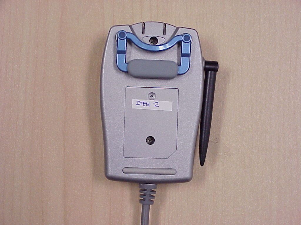
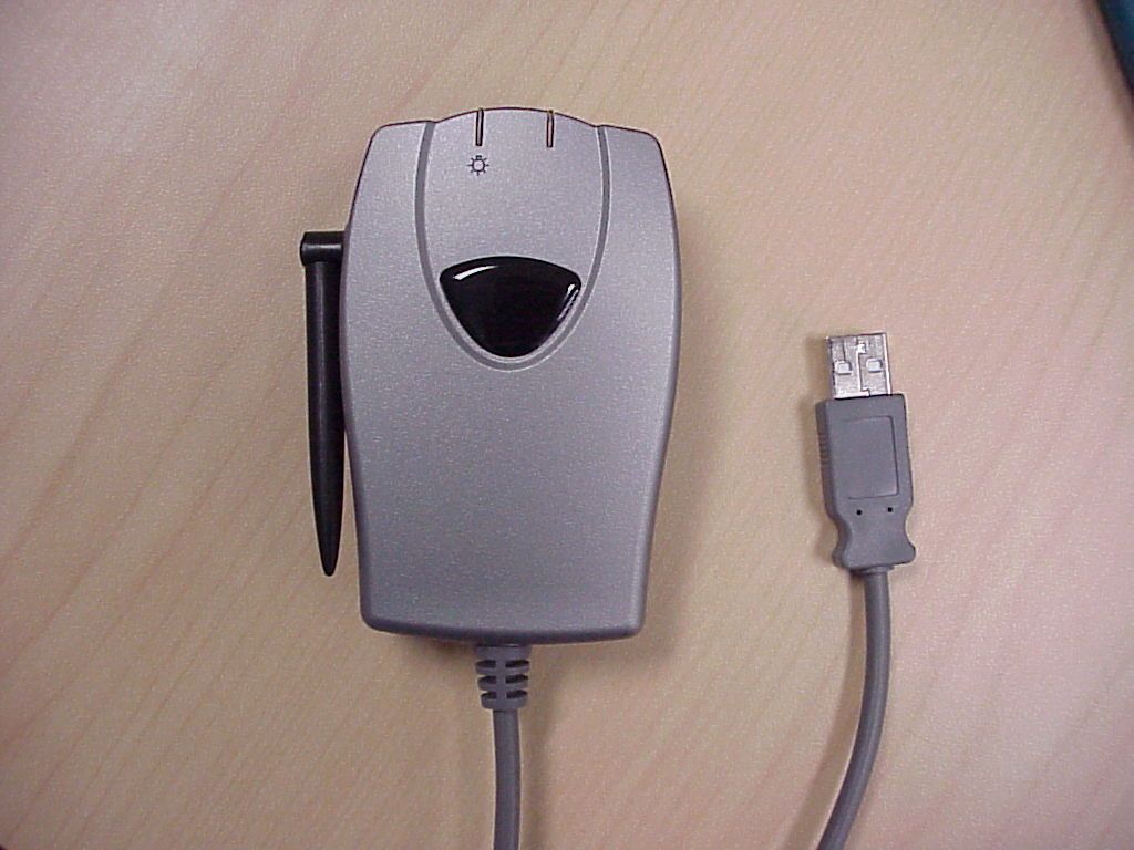
P3BB090H2Bluetooth USB Dongle
Uniwill Computer Corporation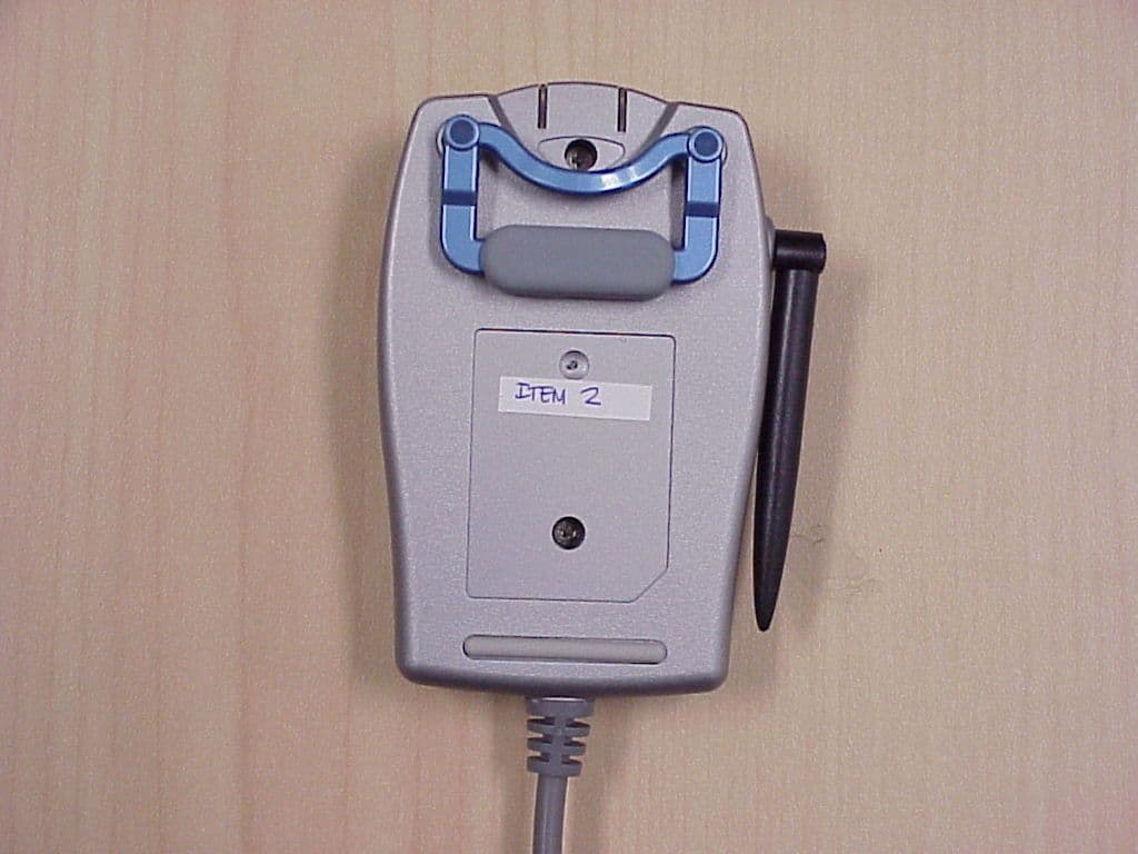
Click to zoom
Application Details
- Equipment Class
- DSS - Part 15 Spread Spectrum Transmitter
- Date of Grant
- Dec 17, 2001
- Application Purpose
- Original Equipment
- Date of Application
- Dec 17, 2001
- Equipment Note
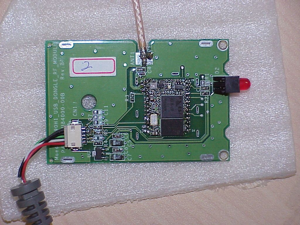
- Bluetooth USB Dongle
- Frequency Range
- 2402.00000000 - 2480.00000000
- Company
- Uniwill Computer Corporation
- Country
- Taiwan
Documents & Files
Document Text
Text extracted from the exhibit documents filed with the FCC. Open a document above to read the original.
Users Manual
Bluetooth USB mini Dongle User’s Manual Before starting installation, be sure to read this user’s manual in detail Steps for Bluetooth USB mini Dongle installation. 1. Please take out the Bluelet software CD-ROM. 2. Insert Bluelet CD-ROM into your PC’s CD-ROM drive, and make sure you have read all instructions for installing Bluelet clearly. Note: ! Before start installation, please make sure there is no other Bluetooth application software in your PC. ! Please do NOT plug in Bluetooth USB mini Dongle before running Bluelet installation program. 3. Following the directions provided with your PC to install the Bluelet application software. (This Bluelet software is enabled for Win98SE, WinME, and Win2000 operating systems.) 4. After you install Bluelet, re-start your PC under Windows operating system. 5. Hold the USB plug of Bluetooth Dongle toward the PC’s USB slot, and keep USB plug the same direction with PC’s USB slot. 6. Firmly press the USB plug into the slot, then the USB mini Dongle will be configured by the operating system automatically. 7. Please follow Bluelet’s user guide to operate Bluetooth USB mini Dongle and enjoy the wireless communication. Federal Communications Commission (FCC) Statement This device has been tested and found to comply with Part 15 of the FCC Rules. Operation is subject to the following two conditions: (1) this device may not cause harmful interference, and (2) this device must accept any interface received, including interface that may cause undesired operation. NOTE: This equipment has been tested and found to comply with the limits for a Class B digital device, pursuant to Part 15 of the F CC Rules. These limits are designed to provide reasonable protection against harmful interference in a residential installation. This equipment generates, uses and can radiate radio frequency energy and, if not installed and used in accordance with the instructions, may cause harmful interference to radio communications. However, there is no guarantee that interference will not occur in a particular installation. If this equipment does cause harmful interference to radio or television reception, which can be determined by turning the equipment off and on, the user is encouraged to try to correct the interference by one or more of the following measures: -- Reorient or relocate the receiving antenna. -- Increase the separation between the equipment and receiver. -- Connect the equipment into an outlet on a circuit different from that to which the receiver is connected. -- Consult the dealer or an experienced radio/TV technician for help. Changes or modifications not expressly approved by Uniwill could void the user's authority to operate the equipment. Exposure to Radio Frequency Radiation The radiated output power of the this internal wireless radio is far below the FCC radio frequency exposure limits. Nevertheless, the wireless radio shall be used in such a manner that the radio is 2.5 cm or further from the human body. The internal wireless radio operates within guidelines found in radio frequency safety standards and recommendations, which reflect the consensus of the scientific community. Uniwill therefore believes the internal wireless radio is safe for use by consumers. The level of energy emitted is far less than the electromagnetic energy emitted by wireless devices such as mobile phones. However, the use of wireless radios may be restricted in some situations or environments, such as aboard airplanes. If you are unsure of restrictions, you are encouraged to ask for authorization before turning on the wireless radio. CE Compliance This device has gained the necessary approvals from independent CE test bodies for electromagnetic compatibility (EMC), immunity and electrostatic discharge (ESD). The device is notified in Germany and Austria. This device complies with the Bluetooth 1.1 specification for USB Uniwill Computer Corp. No.24, Pei-Yua n Rd., Chung Li Ind . Park , C hung Li city, Tao Yua n, Taiwa n, R.O.C. TEL: 886-3-4616000; FAX: 886-3-4618000
Block Diagram
Block Diagram Uniwill Computer Corp.
Cover Letter(s)
Federal Communication Commission Equipment Authorization Division, Application Processing Branch 7435 Oakland Mills Road Columbia, MD 21048 November 15, 2001 TO WHOM IT MAY CONCERN Pursuant to Paragraphs §0.457 and 0.459 of the Commission’s Rules (47 C.F.R.) and Section §552(b)(4) of the Freedom of Information Act, Uniwill Computer Corp. requests confidentiality for the following products: FCC ID P3BB091H1 For the product stated above, we request that the following information be held confidential: 1) Electrical Schematics of the Circuitry No other items submitted as part of the equipment authorization filing process are deemed confidential. The above exhibits contain Uniwill Computer Corp. trade secrets and proprietary information that could be of benefit to our competitors regarding the design of our mobile handset. This material is not customarily available to the general public and we request that it be withheld from public inspection. If you have any questions, please feel free to contact me at the address shown below. Sincerely, Lothar Schmidt Technical Manager EMC/Radio
ID Label/Location Info
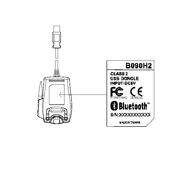
FCCID:P3BB090H2E ! C0682 FCCID:P3BB090H2E!C0682
Operational Description
Bluetooth Solution BTM2010-1 (+20dbm) BTM2010-2 (0dBm) 35mm x 17mm x 2.6mm22mm x 16mm x 2.6mm Bluetooth Module Versatility, Simplification, and true Mobility ! Complies with Bluetooth Specification v1.1 ! Supports Bluetooth Class 1/ Class 2 ! Receiving Signal Range between –85 to –20 dBm ! HCI interface over USB/UART ! Built-in flash memory, system clock ! BQB certificate Uniw ill Bluetooth Module is enabling for devices such as Notebooks, PDAs, Mobile Phones, and PC peripherals, communicate one another by using Bluetooth Technology. Bluetooth Dongle The Uniwill Bluetooth Dongles, B090H2 and mini B091H1, are external adopters for Notebooks and Desktop PCs to communicate one another by using Bluetooth technology. Both Dongles (B090H2 and mini B091H1) support Bluetooth profiles including Generic Access Profile, Serial Port Profile, Service Discovery Application Profile, File Transfer Profile, Dial-up Networking, and LAN Access Profile. In addition, these devices include all the hardware, drivers, and software applications for Win98SE, WinME, and Win2000 operating systems. FeaturesB091H1 Bluetooth mini DongleB090H2 Bluetooth Dongle Operating Distance20m (High sensitivity communication supports) 30m (High sensitivity communication supports) CompliantBluetooth Specification v1.1Bluetooth Specification v1.1 Transmission Power0dBm (Class 2)0dBm (Class 2) Output InterfaceUSB, complies with USB v1.1USB, complies with USB v1.1 Certificate FCC, CE, FCC, CE, Uniwill Computer Corporation Taiwan 14F, No.67, Sec.1, Chung Shan Rd., Hsin Chuang City, Taipei, Taiwan, R.O.C. Tel +886-2-8521-6888 ext 396 Fax +886-2-8521-5666 Email Amber [email protected] B091H1 mini Dongle B090H2 Dongle 87mm x 31mm x 7mm90mm x 68mm x 30mm Weight 16 .1g Weight 95 .8g Uniwill Computer Corporation U.S. Branch Office 48295 Fremont Blvd. Fremont, CA94538 Tel +1-510-580-6888 Fax +1-510-580-5666 Email [email protected]
RF Exposure Info
CETECOM Inc. 411 Dixon Landing Road Milpitas, CA 95035 Federal Communication Commission Authorization and Evaluation Division 7435 Oakland Mills Road Columbia, MD 21046 Attention: Reviewing Engineer The U ni wi ll USB Bl ue tooth do ngle is external USB device using spread spectrum technique for PC applications for wireless connection to other Bluetooth enabled devices etc.. Due to the construction of the dongle and the position at a PC (it’s connected to the USB board and the very low power ) the distance to the body is at least 2.5 cm This information includes the following : A minimum separation distance of 2.5 cm must be maintained between the antenna and the person for this device to satisfy the RF exposure requirements of the FCC. The maximum output power allowed for the Bluetooth radio is 100 mW. Maximum EIRP of the equipment = 2.44 dBm (0.00175 W); equivalent to 3.08 V/m in 10 cm distance Regarding MPE limits, GPUC environment limits maximum exposure to 1 mW/cm 2. The power density is: at 2.5 centimeters from an antenna S = E 2 /3770=-13 H 2 = 0.0223 mW/cm 2 < 1 mW/cm 2 Where: S = Power density (mW/cm 2) E = electrical field strength (V/m) Calculations are based on standard formula for calculating field strength at a distance and converting power density using free space impedance. Compliance is shown for the built in module, which incorporates the antenna on board of the module even for the distance of 2.5 cm. A statement is included in the manual. If you should have any questions regarding this submission, please feel free to contact the undersigned. Yours tr ul y, Lothar Schmidt Technical Manager EMC/Radio CETECOM Inc.
Test Report
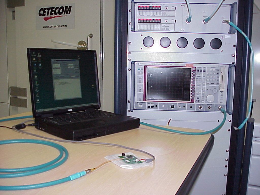
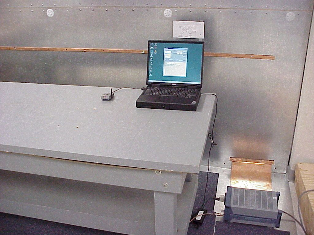
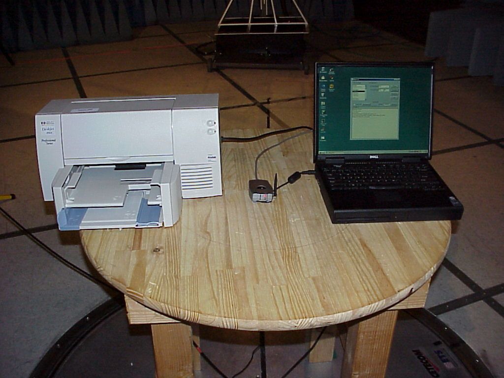
CETECOM Inc. CETECOM Inc. 411 Dixon Landing Road, Milpitas, CA-95035, USA Phone: +1 408 586 6200 Fax: +1 408 586 6299 www.cetecom.com Issued test report consists of 50 Pages Page 1 (50) Test report no.: 191FCC/2001 FCC Part 15.247 (B090H2) FCC LISTED, REG. NO.: 101450 & RECOGNIZED BY INDUSTRY CANADA IC – 3925 CETECOM Inc. Test report no.:191FCC/2001 Issue date:2000-11-01 Page 2 (50) Table of Contents 1 General information 1.1 Notes 1.2 Testing laboratory 1.3 Details of applicant 1.4 Application details 1.5 Test item 1.6 Test standards 2 Technical test 2.1 Summary of test results 2.2 Test report 1 General information 1.1 Notes The test results of this test report relate exclusively to the test item specified in 1.5. The CETECOM Inc. USA does not assume responsibility for any conclusions and generalisations drawn from the test results with regard to other specimens or samples of the type of the equipment represented by the test item. The test report may only be reproduced or published in full. Reproduction or publication of extracts from the report requires the prior written approval of the CETECOM Inc USA. TEST REPORT PREPARED BY: EMC & Radio Engineer: Harpreet Sidhu 1.2 Testing laboratory CETECOM Inc. 411 Dixon Landing Road, Milpitas, CA-95035, USA Phone: +1 408 586 6200 Fax: +1 408 586 6299 E-mail: [email protected] Internet: www.cetecom.com CETECOM Inc. Test report no.:191FCC/2001 Issue date:2000-11-01 Page 3 (50) 1.3 Details of applicant Name : Uniwill Computer Corp. Street : 14F, No. 67, Sec-1, Ching Shan Rd., Hsiy Chang City City : Taipei Country : Contact : Taiwan Tony Kuan Telephone : +886 2 852 16 888 Ext.-357 Telefax : +886 2 852 15 666 e-mail : [email protected] 1.4 Application details Date of receipt of application : 2001-09-10 Date of receipt of test item : 2001-09-21 Date of test : 2001-09-28, 2001-10-01/05 1.5 Test item Manufacturer : Applicant Name of EUT : B090H2 USB Dongle Description : Class-2 BT Module Model No. : B090H2 Serial No. : FCC ID : N/A Additional informations Frequency : 2.402 – 2.480 GHz Type of modulation : FHSS Number of channels : 79 Antenna : External Power supply : Via USB Output power : 0 dBm Extreme Vol. Limits : Extreme Temp. Limits : 0°C - +35°C 1.6 Test standards: FCC Part 15 §15.247 CETECOM Inc. Test report no.:191FCC/2001 Issue date:2000-11-01 Page 4 (50) 2 Technical test 2.1 Summary of test results No deviations from the technical specification(s) were ascertained in the course of the tests performed. Technical responsibility for area of testing : 2001-11-01 EMC & Radio Lothar Schmidt Date Section Name Signature CETECOM Inc. Test report no.:191FCC/2001 Issue date:2000-11-01 Page 5 (50) 2.2 Testreport TEST REPORT Test report no. : 191FCC/2001 (B090H2) CETECOM Inc. Test report no.:191FCC/2001 Issue date:2000-11-01 Page 6 (50) TEST REPORT REFERENCE LIST OF MEASUREMENTS Paragraph PARAMETER TO BE MEASURED PAGE Transmitter parameters § 15.204 Antenna gain 7 § 15.247 (a) Carrier frequency separation 8 § 15.247 (a) Number of hopping channels 9 § 15.247 (a) Time of occupancy (dwell time) 13 § 15.247 (a)(1) Spectrum Bandwith of a FHSS System 16 § 15.247 (b)(2) Maximum peak output power 20 §15.247 Band edge compliance 28 § 15.247 (c)(1) Emission limitations 30 § 15.107/207 AC Line Conducted Emission 43 Receiver parameters § 15.209 Spurious radiations - Radiated 45 Test equipment listing 50 CETECOM Inc. Test report no.: 191FCC/2001 Issue Date: 2001-11-01 Page 7 (50) Antenna Gain SUBCLAUSE § 15.204 The max gain is +4.45dBi (measured effectiv radiated power – measured conducted power with a temporary RF-connector) CETECOM Inc. Test report no.: 191FCC/2001 Issue Date: 2001-11-01 Page 8 (50) CARRIER FREQUENCY SEPERATION §15.247(a) CETECOM Inc. Test report no.: 191FCC/2001 Issue Date: 2001-11-01 Page 9 (50) NUMBER OF HOPPING CHANNELS §15.247(a) The number of hopping channels is 79 (see next 4 plots) The right red line corresponds to the left red line from the next plot. Plot 1: Total 23 CETECOM Inc. Test report no.: 191FCC/2001 Issue Date: 2001-11-01 Page 10 (50) Plot 2: Total 25 CETECOM Inc. Test report no.: 191FCC/2001 Issue Date: 2001-11-01 Page 11 (50) Plot 3: Total 19 CETECOM Inc. Test report no.: 191FCC/2001 Issue Date: 2001-11-01 Page 12 (50) Plot 4: Total 12 CETECOM Inc. Test report no.: 191FCC/2001 Issue Date: 2001-11-01 Page 13 (50) TIME OF OCCUPANCY (DWELL TIME) FOR DH1 §15.247(a) The system makes worst case 1600 hops per second or 1 time slot has a length of 625μs with 79 channels. A DH1 Packet need 1 time slot for transmitting and 1 time slot for receiving. Then the system makes worst case 800 hops per second with 79 channels. So you have each channel 10.13 times per second and so for 30 seconds you have 303.9 times of appearence . Each Tx-time per appearence is 501μs. So we have 303.9 * 501 μs = 152.25 ms per 30 seconds. CETECOM Inc. Test report no.: 191FCC/2001 Issue Date: 2001-11-01 Page 14 (50) TIME OF OCCUPANCY (DWELL TIME) FOR DH3 §15.247(a) A DH3 Packets need 3 time slots for transmit and 1 for receicing, then the system makes worst case 400 hops per second with 79 channels. So you have each channel 5.1 times per second and so for 30 seconds you have 153 times of appearence . Each Tx-time per appearence is 1.73 ms. So we have 153 * 1.73 ms = 264.69 ms per 30 seconds. CETECOM Inc. Test report no.: 191FCC/2001 Issue Date: 2001-11-01 Page 15 (50) TIME OF OCCUPANCY (DWELL TIME) FOR DH5 §15.247(a) At DH5 Packets you need 5 time slots for transmit and 1 for receicing,then the system makes worst case 266,7 hops per second with 79 channels. So you have each channel 3.36 times per second and so for 30 seconds you have 100,8 times of appearence . Each tx-time per appearence is 2.98 ms. So we have 100.8 * 2.98ms = 300.384 ms per 30 seconds. CETECOM Inc. Test report no.: 191FCC/2001 Issue Date: 2001-11-01 Page 16 (50) SPECTRUM BANDWIDTH OF FHSS SYSTEM §15.247(a) 20 dB bandwidth TEST CONDITIONS 20 dB BANDWIDTH ( kHz ) Frequency (MHz) 2…
Text truncated - open the document above for the full version.
Test Report
EXHIBIT BB – Processing Gain FCC ID O2Z-BT2 Page 1 of 11 Properties/Title v2 15 February 2001 MEMORANDUM – PROCESSING GAIN REPORT FOR INTEL(R) PERSONAL WIRELESS MODULE Subject: Results of Processing Gain Tests for FCC Qualification 1 INTRODUCTION This memo presents the results of the Processing Gain (PG) tests carried out for FCC qualification of the Intel(R) Personal Wireless Module chip. The FCC states that the PG from a hybrid Bluetooth receiver must be greater than 17 dB when measured in accordance with the Continuous Wave (CW) jamming margin method. Testing of the Intel(R) Personal Wireless Module “B” Bluetooth chip has found the PG due to the DS section to be approximately 5 dB and the PG due to the FH part to be approximately 15 dB. It is therefore concluded that the Intel(R) Personal Wireless Module Bluetooth Chip complies with the FCC PG requirements for radio communication systems. The rest of this paper outlines the PG measurement technique and discusses the test results. Appendix A contains a list of test equipment and Appendix B contains a printout of the measurement results. 2 METHOD 2.1 PG Definition The Processing Gain from a frequency hopping communication system is derived from two parts, the FH section and the DS section. The PG due to FH is given by a simple equation and is constant. However measurement of the PG due to DS is a little more complex. One technique is to use the CW jamming margin method. This method measures PG due to DS using the following algorithm: A CW signal generator is stepped in 50kHz increments across the passband of the system, recording at each point the generator level required to produce the 0.1% Packet Error Rate (PER). This is the jammer level. This level is then referenced to the output power of the intended Bluetooth signal and the Jammer to Signal Ratio JSR is thus calculated. The worst 4 JSR measurements are discarded and the worst remaining JSR is used to calculate the PG due to DS as follows: sysp LJSRSNRG++= min Page 2 of 11 Properties/Title v2 15 February 2001 where G p = the processing gain of the system, SNR = the signal to noise ratio required for 0.1% BER, JSR min = minimum J/S ratio and L sys = system losses. 2.2 PG Measurement Technique Figure 1 provides an overview of the PG measurement technique. The measurement is performed in two parts, measurement of the system SNR and measurement of JSR min . Figure 1: PG Measurement Technique The system SNR is calculated using the following algorithm. Generate Bluetooth PRBS-9 packets using a Bluetooth chip emulator (1) and a Vector Signal Generator (2). Combine this signal with white noise of a constant level, which is generated using a noise source (4) and a CW Signal Generator (3). Then vary the level of the Bluetooth signal until the BER measured by the Bluetooth chip (7) is 0.1%. The resulting SNR is the signal level divided by the Noise level. Page 3 of 11 Properties/Title v2 15 February 2001 The JSR for a given jamming frequency is calculated using the following algorithm. Generate Bluetooth PRBS-9 packets using the Bluetooth chip emulator (1) and the Vector Signal Generator (2). Combine this signal with a constant CW tone at the jamming frequency using a CW Signal Generator (5) and a combiner (6). Then vary the level of the Bluetooth signal until the PER measured by the Casira Bluetooth Module (7) is 0.1%. The resulting JSR is the signal level divided by the jamming level. 3 RESULTS 3.1 Overview The measurements found that the PG due to DS caused by the access code in page and inquiry mode is found to be approximately 5dB when the access code is a relatively random mixture of 1's and 0's. A random access code causes the most Inter Symbol Interference (ISI) and hence the worst PG for a hybrid system. Therefore only the results for this access code are used in the PG calculation. The PG due to FH is given as PG FH = 10 log 10 (number of frequency hops) The number of hops in a Bluetooth system is 32, therefore the PG due to FH is approximately 15 dB. When this is added to the PG due to DS, the total PG for the Bluetooth chip is approximately 20 dB, above the minimum PG requirement for FCC qualification. 3.2 Detailed Results Test Date: 17/11/00 Sample Time: 30 seconds Access Code: c6967e Signal Frequency: 2.432GHz Receiver Sensitivity: -88.7 dBm Jammer Signal Level: -85.7 dBm Measured SNR: 18.8dB System Losses: 2dB To calculate processing gain, ignore the worst 20% of data points and then apply the following formula: Page 4 of 11 Properties/Title v2 15 February 2001 sysp LJSRSNRG++= min Where G p = Processing Gain of the module SNR = signal to noise ratio of the module JS min = minimum J/S ratio after the worst 20% of J/S samples have been discarded L sys = System losses A total of 20 samples were taken by stepping the jamming signal frequency offsets in 50kHz increments over the bandwidth of the receiver. The worst 4 samples were found at –500kHz, -450kHz, -400kHz and 500kHz and were discarded. The remaining minimum J/S ratio was found to be -15.4dB at an offset of +350kHz Thus, the processing gain due to direct sequence spreading in page and inquiry mode is dBG p 4.524.158.18=+−= -500-400-300-200-1000100200300400500 -30 -25 -20 -15 -10 -5 0 5 Jamming Frequency Offset (kHz) J/S (dBs) J/S ratio performance for Processing Gain FCC Testing Page 5 of 11 Properties/Title v2 15 February 2001 APPENDIX A - TEST EQUIPMENT LIST Reference: Instrument Type Name 1 Bluetooth IC Emulator Board N/A 2 Vector Signal Generator IFR2052 3 CW Signal Generator IFR2025 4 White Noise Generator HP33120A 5 RF Mixer M8HC-7 6 RF Combiner 6 dB loss combiner 7 Bluetooth Motherboard and Bluetooth chip Module Bluetooth Development Kit 8 5V, 4A DC Power Supply N/A 9 Spectrum Analyser HP E4405B Page 6 of 11 Properties/Title v2 15 February 2001 APPENDIX B - TEST RESULTS Timestamp: 14:42.43, 16/11/2000 Signal Freq = 2.432 GHz Jammer Level = -85.7 dBm Jammer Offset = -500 kHz Level = -68.7 dBm BER = 0.03% PER = 0.01% …
Text truncated - open the document above for the full version.
Contact Information
Applicant
Amber Huang(Product Manager)
Technical Contact
411 Dixon Landing RoadLothar Schmidt
[email protected]408-586-6214
411 Dixon Landing Road · Milpitas, California · United States
Non-Technical Contact
411 Dixon Landing RoadLothar Schmidt
[email protected]408-586-6214
Test Firm
Cetecom Inc.Lothar Schmidt
Technical Specifications
| # | Rule Parts | Frequency Range | Power Output |
|---|---|---|---|
| 1 | 15C | 2.40 GHz - 2.48 GHz | 1.75 mW |
Other Applications from Uniwill Computer Corporation
P3B755SI4
Jan 04, 2005Notebook Computer W/ 802.11b/g WLAN
Equipment Class
DTS - Digital Transmission System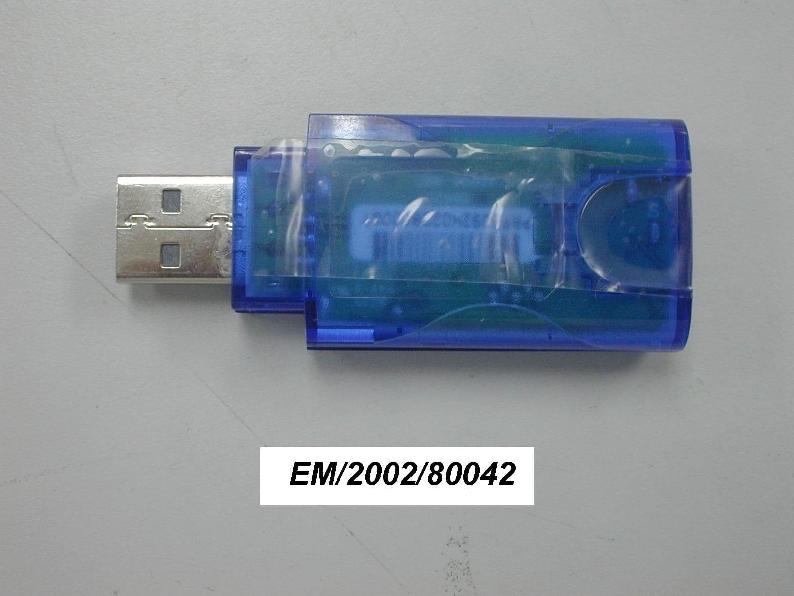
P3BB092H0
Oct 13, 2002Mini Bluetooth USB Dongle
Equipment Class
DXX - Part 15 Low Power Communication Device Transmitter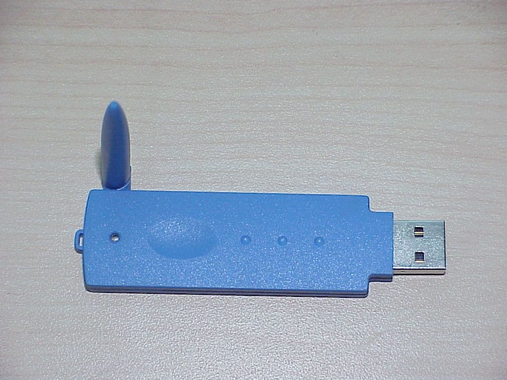
P3BB091H1
Dec 17, 2001Bluetooth USB mini Dongle
Equipment Class
DSS - Part 15 Spread Spectrum Transmitter