P5G-368-397-YY-PICommunication Connector for Playstation
Bitswave, Inc.
Click to zoom
Application Details
- Equipment Class
- DXT - Part 15 Low Power Transceiver, Rx Verified
- Date of Grant
- Dec 08, 2002
- Application Purpose
- Original Equipment
- Date of Application
- Dec 08, 2002
- Equipment Note
- Communication Connector for Playstation
- Frequency Range
- 910.70000000 - 917.70000000
- Company
- Bitswave, Inc.
- Country
- United States
Documents & Files
Document Text
Text extracted from the exhibit documents filed with the FCC. Open a document above to read the original.
Users Manual
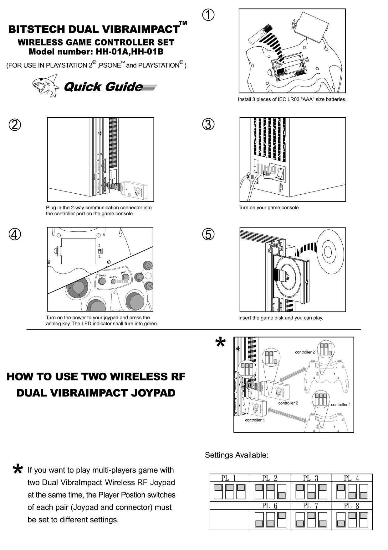
Warranty Information We offer one (1) year warranty from the date of purchase or receipt of the warranty form, whichever is earlier subject to the terms and conditions set out below: This warranty does not cover damage due to external causes, including accident, abuse, misuse, problems with electrical power, servicing not authorized by BitsTech, usage not in accordance with product instructions, failure to perform required preventive maintenances, and problems caused by use of parts and components not supplied by BitsTech. BitsTech will repair or replace products covered under this limited warranty that are returned to BitsTech’s facility. To request warranty service, you must first send e-mail to Customer Technical Support at [email protected] within the warranty period. If warranty service is required, BitsTech will issue a Return Material Authorization Number (RMA No.) and receiving address for this product. You must then ship the products back to BitsTech in their original or equivalent packaging, including all materials contained in the same as you purchased this item, prepay shipping charges, and insure the shipment or accept the risk of loss or damage during shipment. Please clearly mark RMA No. and “WARRANTY RETURN” o the shipping box. You must also enclose copy of the original invoice and spell out the reason(s) for returning the products. BitsTech will ship the repaired or replacement products to you freight prepaid if you use an address in Hong Kong SAR. Shipments to other locations will be made freight collect. NOTE: Only packages that have been assigned a RMA number by technical support will be accepted. General Provisions BitsTech makes no express warranties beyond those stated in their s warranty statements. BitsTech disclaims all other warranties, express or implied, including without limitation implied warranties of merchantability and fitness for a particular purpose. BitsTech’s Responsibility for malfunctions and defects in hardware is limited to repair and replacement as set forth in this warranty statement. BitTech does not accept liability beyond the remedies set forth in this warranty statement or liability for incidental or consequential damages, including without limitation any liability for products not being available for use or for lost data or software. Warring This equipment has been tested and found to comply with the limits for a Class B digital device, pursuant to Part 15 of the FCC Rules. These limits are designed to provide reasonable protection against harmful interference in a residential installation. This equipment generates, uses and can radiate radio frequency energy and, if not installed and used in accordance with the instructions, may cause harmful interference to radio communications. However, there is no guarantee that interference will not occur in a particular installation. If this equipment does cause harmful interference to radio or television reception, which can be determined by turning the equipment off and on, the user is encouraged to try to correct the interference by one or more of the following measures: - Reorient or relocate the receiving antenna. - Increase the separation between the equipment and receiver. - Connect the equipment into an outlet on a circuit different from that to which the receiver is connected. - Consult the dealer or an experienced radio/TV technician for help. This device complies with Part 15 of the FCC Rules. Operations in subject to the following conditions: 1. This device may not cause harmful interference, 2. This device must accept any interference received including interference that cause undesired operation. Disclaimer This equipment complies with Part 15 of the FCC Rules. Any changes or modifications mot expressly approved by the manufacturer could void the users authority to operate the equipment. This product is not produced or authorized to produce by Sony Corporation nor under its supervision. In particular when this product is use to play games; the function of each of the buttons may be different from that of the buttons of the joypad produced by Sony. No liability whatsoever would be accepted in this respect. Customer Technical Support/Customer Service (for questions, trouble shooting, or additional instructions: [email protected] ) PlayStation, PlayStation2, PS One, and Dual Shock are trademarks and/or registered trademarks of Sony Computer Entertainment, Inc. All other trademarks are properly of their respective owners. Contents, designs and specifications are subject to change without notice and may vary from one country to other. Design Registration & Patent Pending All rights reserved. BisTech Inc. 2001
Block Diagram
900-907 MHz 10.7MHz 910.7 – 917.7 MHz 10 MHz
Cover Letter(s)
B B B i i i t t t s s s W W W a a a v v v e e e , Inc. 10700 Corporate Dr. Stafford, TX 77477, USA Tel (281) 277-8689 Fax (281) 277-8677 www.bitswavepower.com Suite 1503, 15 th Floor Tung Ning Building No. 2 Hillier Street, Sheung Wan Hong Kong SAR Tel 852 2668 9801 Fax 852 2670 8429 REQUEST FOR CONFIDENTIALITY Bitswave, Inc. would like to request confidentiality with regard to the following documents in the filing for equipment approval identified by FCC ID. No. P5G-368-397-YY (1) Schematic diagrams contained in electronic file identified as schematics.doc. It is the opinion of Bitswave, Inc. disclosure of this information would result in significant loss of revenue. This information should be kept confidential for 5 years. Richard Liu Bitswave, Inc. 10701 Corporate Dr. Stafford, Texas 77477
Cover Letter(s)
B B B i i i t t t s s s W W W a a a v v v e e e , Inc. 10700 Corporate Dr. Stafford, TX 77477, USA Tel (281) 277-8689 Fax (281) 277-8677 www.bitswavepower.com Suite 1503, 15 th Floor Tung Ning Building No. 2 Hillier Street, Sheung Wan Hong Kong SAR Tel 852 2668 9801 Fax 852 2670 8429 Federal Communications Commission 7435 Oakland Mills Road Columbia, MD 21046 USA Authority to Act as Agent to the Federal Communications Commission On our behalf, I appoint Nemko Dallas, Inc. to act as agent in the preparation of this application for equipment authorization to the Federal Communications Commission. I certify that submitted Exhibits properly describe the device or system for which equipment authorization is sought. I also certify that each unit manufactured, imported or marketed, as defined in the Commission's regulations will have affixed to it a label identical to that submitted for approval with this application. APPLICANT ANTI-DRUG ABUSE CERTIFICATION: In signing this letter, Applicant certifies that, in the case of an individual applicant, he or she is not subject to a denial of federal benefits, that includes FCC benefits, pursuant to Section 5301 of the Anti-Drug Abuse Act of 1988, 21 U.S.C. 853(a), or, in the case of a non-individual applicant (e.g. corporation, partnership or other unincorporated association), no party to the application is subject to a denial of federal benefits, that includes FCC benefits, pursuant to that section. For the definition of a "party" for these purposes, see 47 CFR 1.2002(b). Dated this 3rd Day of January 2002 Agency agreement expiration date: By: Richard Liu, Ph.D., PE Title: Vice President Telephone: 281-277-8689 Applicant:
Cover Letter(s)
RE: Bitswave Inc. FCC ID: P5G-368-397-YY-PI After a review of the submitted information, I have a few comments on the above referenced Application. 1)The block diagram should show the frequencies of all oscillators in the TX portion of the device (CFR 2.1033(a)(5)). Please provide an updated version that includes this information. I have uploaded a block diagram with the oscillator frequencies shown. 2) Although these both parts of the system may have been tested together, please note that the FCC requires a separate FCC ID for each part of this system. This device will require 2 separate ID numbers, one for the joypad, and one for the PS2-Plugin. The only acceptation to this rule is cordless phones (defined that attached to the public switched network directly). Please clarify which part of the system should be uploaded under this ID number given in this application. Unfortunately, a new submittal will be required for the other part of the system that includes updated exhibits for documents referencing the other FCC ID (such as labeling, cover letters, etc.). A separate submission was uploaded to the ATCB site for the joypad under the ID number P5G- 368-397-YY. The joypad submission is still pending. 3) The users manual exhibit is unreadable. Please provide a new exhibit for the users manual. A readable version of the manual has been uploaded. 4) Please note that since labeling information and test photographs were only provided for the PS2-Plugin, only the test report for the plug-in has been reviewed at this time. See note on (2) 5) Please explain how the EUT was tested for average emissions > 1 GHz (appears to only have been tested at 1.8 GHz & 2.7 GHz for average measurements). The device states that it was transmitting in normal mode. From the theory of operation, this device sends a command sent every 16 ms (duration unknown). Please note that it is likely that reduction of the VBW will not be allowed down to 10 Hz. The VBW may only be reduced down to the point that each sweep totally captures an entire single transmission pulse. The sweep may not be reduced to the point that it captures the on-off nature of the transmitter. Note that the FCC requests that a transmitter be placed into a 100% duty cycle for purposes of the measurement when possible. Once a proper trace has been captured using a reduced VBW that still captures 1 entire transmission stated here, additional correction may be applied mathematically for the worse case duty cycle of the transmitter. Please provide detailed information as to how the average measurements were made. Normal operation for this device is one transmission session every 16 ms. In each session the plug-in transmits for 2 ms and the joypad transmits for 4 ms. For this testing the units were set to transmit these data packets continuously. The emissions were all measured with a peak detector (1 MHz RBW/ 1 MHz VBW) and the average limit was applied. If the emission was above the average limit then the emission was re-measured average. A revised report has been uploaded with duty cycle information and with the peak data mathematically corrected for duty cycle.
Cover Letter(s)
American Telecommunications Certification Body Inc. 6731 Whittier Ave, McLean, VA 22101 November 6, 2002 RE: Bitswave Inc. FCC ID: P5G-368-397-YY-PI After a review of the submitted information, I have a few comments on the above referenced Application. 1) The block diagram should show the frequencies of all oscillators in the TX portion of the device (CFR 2.1033(a)(5)). Please provide an updated version that includes this information. 2) Although these both parts of the system may have been tested together, please note that the FCC requires a separate FCC ID for each part of this system. This device will require 2 separate ID numbers, one for the joypad, and one for the PS2-Plugin. The only acceptation to this rule is cordless phones (defined that attached to the public switched network directly). Please clarify which part of the system should be uploaded under this ID number given in this application. Unfortunately, a new submittal will be required for the other part of the system that includes updated exhibits for documents referencing the other FCC ID (such as labeling, cover letters, etc.). 3) The users manual exhibit is unreadable. Please provide a new exhibit for the users manual. 4) Please note that since labeling information and test photographs were only provided for the PS2-Plugin, only the test report for the plug-in has been reviewed at this time. 5) Please explain how the EUT was tested for average emissions > 1 GHz (appears to only have been tested at 1.8 GHz & 2.7 GHz for average measurements). The device states that it was transmitting in normal mode. From the theory of operation, this device sends a command sent every 16 ms (duration unknown). Please note that it is likely that reduction of the VBW will not be allowed down to 10 Hz. The VBW may only be reduced down to the point that each sweep totally captures an entire single transmission pulse. The sweep may not be reduced to the point that it captures the on-off nature of the transmitter. Note that the FCC requests that a transmitter be placed into a 100% duty cycle for purposes of the measurement when possible. Once a proper trace has been captured using a reduced VBW that still captures 1 entire transmission stated here, additional correction may be applied mathematically for the worse case duty cycle of the transmitter. Please provide detailed information as to how the average measurements were made. Timothy R. Johnson Examining Engineer mailto: [email protected] The items indicated above must be submitted before processing can continue on the above referenced application. Failure to provide the requested information may result in application termination. Correspondence should be considered part of the permanent submission and may be viewed from the Internet after a Grant of Equipment Authorization is issued. Please do not respond to this correspondence using the email reply button. In order for your response to be processed expeditiously, you must submit your documents through the AmericanTCB.com website. Also, please note that partial responses increase processing time and should not be submitted. Any questions about the content of this correspondence should be directed to the sender.
Operational Description
Wireless Joypad for Sony PlayStation Theory of Operation 1/4/02 Bitswave, Inc. 1. Station Side Radio The radio system is mainly composed of three parts: radio modem, frequency synthesizer and baseband microprocessor. The radio is interfaced with Sony PlayStation via a 9-pin connector. Sony PayStation sends a command to the radio every 16 milliseconds. The radio takes the data from PlayStation, packetize the data by adding preambles, frame information, and error checking bytes. The packetized frame is transmitted to the wireless joystick. When joystick replies, this radio receives the data, un-packetize it, and sends to Sony PlayStation. The radio modem is a FSK modem running at 78 kbps with Manchester encoding to avoid frequency drifting. Frequency is controlled by a frequency synthesizer which adjusts a voltage-controlled RF oscillator dynamically for accurate frequency management. Channel is set by selecting a 3-position dipswitch. A total of 8 channels can be selected conversing the frequency range of 910.7 – 917.7 MHz. The antenna is an embedded PCB antenna antenna matching is done by using lumped inductors and capacitors. The radio is a half-duplex system and is powered by a 3.3V power source provided by Sony PlayStation. The total average power consumption of the radio system is about 20 mA at 3.3V. 2. Joypad Side Radio Joypad side radio operates in similar way to Station Side Radio as described in previous section. However, this radio works as a slave compared to the Station Side Radio. When powered on, this radio is in receiving mode and waits until a command from Station Side Radio is received. It scans keystrokes on the joypad and replies the command with the keystroke data to the Station Side Radio. Similarly, the data is packetized in the same way as Station Side Radio. The joypad radio is powered by 3-AAA side batteries and down regulated to 3.3V. Another power regulator (3.0V) provides power for two vibration motors in the joypad.
Schematics
CLOCK J51CON1 1 C51 10n J1CON1 1 J133 1 J7CON1 1 R7 100 R14 10 J21CON1 1 Rx_Enable J108CON1 1 C44 0.1u J31CON1 1 C6810n C5710n R15 7.5k J12CON1 1 J49CON1 1 L12 10nH J24CON1 1 J121 1 J63CON1 1 <Doc> <RevCode> PS Side Radio B 12 Monday, November 26, 2001 TitleSize Document Number Rev Date: Sheet of J43CON1 1 C71 10n J80CON1 1 J104CON1 1 J47CON1 1 J83CON1 1 R5 10 J14CON1 1 J72CON1 1 J69CON1 1 J3CON1 1 J40CON1 1 3.6V + C39 4.7u J33CON1 1 J124 1 Tx_In Q2 CDF107B-A0 C6610n J102CON1 1 J45CON1 1 F-Diviation C6522 J6CON1 1 J99CON1 1 J28CON1 1 C4318 J64CON1 1 C60 10n U8 LMX1601 12345678 16151413121110 9 FoLD OSC_IN OSC_OUT GND FIN_AX VCC_AXCPO_AX EN_AX CLOCKDATALEGNDFIN_MAINVCC_MAINCPO_MAINEN_MAIN RF2945 12345678 9 10 11 12 13 14 15 16 2423222120191817 32 31 30 29 28 27 26 25 TX_ENTX_OUTGND1RX_INGND2LNA_OUTGND3MIX_IN GND5 MXO VBG RSSI IF1_IN CPB1+ CPB1- IF1OUT RESNTR+ MOD_IN DATA REF DEMOD_IN GND6 CBP2- CBP2+IF2_IN RX_EN LV_ADJ VCC3 DATA_OUT VCC1 GND4 VCO_OUT RESNTR- J127 1 J107CON1 1 J73CON1 1 J103CON1 1 R122k J66CON1 1 J5CON1 1 C5222 C58 22 J13CON1 1 J115 1 C21n J44CON1 1 J126 1 3.6V C50 22 J91CON1 1 J22CON1 1 J4CON1 1 J101CON1 1 J116 1 J8CON1 1 L14 8.2uH LE J27CON1 1 J48CON1 1 J61CON1 1 J37CON1 1 C254 J60CON1 1 SK107M1-AE-10X 1 2 3 J18CON1 1 J129 1 J113 1 J81CON1 1 L10 6.8n J74CON1 1 J77CON1 1 R25 5k R92.7k J50CON1 1 L13 SK107M1-AE-10X 1 2 3 C41 22 J117 1 J30CON1 1 Rx_Out J93CON1 1 J87CON1 1 C6710n J131 1 J52CON1 1 J2CON1 1 J38CON1 1 Q1 10MHz J76CON1 1 J65CON1 1 J105CON1 1 C533 C5947n C544.7n J11CON1 1 J68CON1 1 J17CON1 1 R8 11k J26CON1 1 J78CON1 1 FoLD R10 3.6k J54CON1 1 J98CON1 1 J20CON1 1 J111 1 J100CON1 1 J122 1 J70CON1 1 J92CON1 1 3.6V Tx_Enable C45 22 J46CON1 1 J132 1 R11 10 J41CON1 1 J82CON1 1 J59CON1 1 D2 KV1848k C6410n J123 1 J89CON1 1 L7 8.2nH J23CON1 1 J79CON1 1 C56 2.2n J88CON1 1 J128 1 L11 6.8nH 3.6V C47 0.1u C42 22 J90CON1 1 J19CON1 1 3.6V J9CON1 1 C4010n J114 1 J16CON1 1 J110 1 DATA J112 1 C70 11 J130 1 C72 22 J75CON1 1 J53CON1 1 C61 10n J71CON1 1 + C634.7u J55CON1 1 J120 1 C133 J39CON1 1 C62 10 J42CON1 1 J97CON1 1 J106CON1 1 J96CON1 1 C46 22 J125 1 J32CON1 1 J85CON1 1 J36CON1 1 J62CON1 1 J57CON1 1 J15CON1 1 J10CON1 1 3.6V C55 22 J34CON1 1 J58CON1 1 C290 J35CON1 1 J94CON1 1 J25CON1 1 R231.1k J84CON1 1 J95CON1 1 C234 J67CON1 1 J118 1 J29CON1 1 C48 0.1u J119 1 R100 2k J56CON1 1 R6 10 J86CON1 1 Rx_EnableFoLD C781uF C7318p CLOCK Bitswave 002 1.0 PS Side Controller B 22 Monday, November 26, 2001 TitleSize Document Number Rev Date: Sheet of Dout Y120 M Tx_EnableLE ACK L16FB uC 3.6 V DATA ACK U18 EM78P451AQ 123456789 1011 3332313029282726252423 44 43 42 41 40 39 38 37 36 35 34 12 13 14 15 16 17 18 19 20 21 22 P90P91P92P93P94P95P50P51P52P53P54 P71P72P67P66P65P64P63P62P61P60P87 CLK DATA /INT VSS OSCO R-OSCI VDD NC NC NC P70 P55 P56 P57 P80 P81 NC P82 P83 P84 P85 P86 C771uF R10110 K SCLK S1TX/RX Channel Select 123 654 R10410 K SCLK C7418p PS 3.3 V Rx_Out Dout C3100n PS 3.3 V + C76100uF Din D3LED Din PS 3.3 V 3.6V Tx_In CS CS R10310 K uC 3.6 V PS 3.3 V R105331 J109CON9 123456789 R10210 K R5 1k S17 INTERSECTION FoLD R10Lx DATA S8ANALOG S10 UP Q12N2222A R210 K Bitswave 001 1.0 Joy Controller C 11 Thursday, October 18, 2001 TitleSize Document Number Rev Date: Sheet of C410uF S16 DOWN +3V C1010n + C74.7u C50.01uF S7 R1 TX_ENABLE +3.3V U1 EM78P451AQ 123456789 1011 3332313029282726252423 44 43 42 41 40 39 38 37 36 35 34 12 13 14 15 16 17 18 19 20 21 22 P90P91P92P93P94P95P50P51P52P53P54 P71P72P67P66P65P64P63P62P61P60P87 CLK DATA /INT VSS OSCO R-OSCI VDD NC NC NC P70 P55 P56 P57 P80 P81 NC P82 P83 P84 P85 P86 D41N5817(DO-41) M2MOTOR AC S3SELECT J1CON12A 1357911 2468 1012 RX_ENABLE S1TX/RX Channel Select 123 654 TX_IN S18Power FoLD Y18 M DATA LE M1MOTOR AC R310 K +3V C50.01uF R622 S13 RIGHT S15 CIRCLE LE + C910u +3.3V R8Rx S12 LEFT D11N4001 CLOCK Q22N2222A S14 SQUARE BT14.5V C50.01uF R110 K RX_OUT +3V R3810 K U2TK11133CS 123 54 CTLGNDBPS Vin Vout R722 C810n C133 p +3.3V D21N4001 RX_ENABLE RX_OUT +3.3V S11 TRIANGLE U3TK11230CS 123 54 CTLGNDBPS Vin Vout S7 R3 C233 p R9Ry R11Ly TX_ENABLE + C610u C50.01uF C310uF R3710 K S5 R2 S9START TX_IN +3.3V S6 L1 CLOCK D3LED S6 L3 S4 L2 +3.3V 3.6V C11 J49CON1 1 J79CON1 1 J6CON1 1 R14 10 J70CON1 1 C5222 J20CON1 1 C533 J24CON1 1 + C634.7u C5710n R100 2k J56CON1 1 C254 C58 22 J19CON1 1 J5CON1 1 CLOCK R7 100 J106CON1 1 R1 3.3k J40CON1 1 J95CON1 1 R6 10 R25 5k R92.7k J107CON1 1 C71 10n C4010n J71CON1 1 R11 10 Rx_Out Tx_Enable J75CON1 1 C46 22 Tx_In CLOCK C48 0.1u J37CON1 1 J48CON1 1 J22CON1 1 C60 10n J86CON1 1 C55 22 C50 22 L13 FFE1070MA R 1 2 3 J59CON1 1 J98CON1 1 J83CON1 1 3.6V L10 6.8n J74CON1 1 J65CON1 1 J38CON1 1 J62CON1 1 <Doc> <RevCode> Radio Stick Side B 11 Sunday, December 16, 2001 TitleSize Document Number Rev Date: Sheet of J39CON1 1 J69CON1 1 J43CON1 1 L12 10nH J60CON1 1 J8CON1 1 D2 KV1848k C61 10n J16CON1 1 3.6V J28CON1 1 J64CON1 1 3.6V J35CON1 1 J17CON1 1 J85CON1 1 FoLD C70 11 C6410n J50CON1 1 J80CON1 1 J82CON1 1 L11.8nH J47CON1 1 J32CON1 1 J11CON1 1 C62 10 J42CON1 1 F-Diviation J2CON1 1 C41 22 J29CON1 1 Rx_Enable Tx_In J78CON1 1 DATA J92CON1 1 J99CON1 1 + C39 4.7u C4318 J46CON1 1 J30CON1 1 J55CON1 1 FFE1070MA R 1 2 3 J103CON1 1 J51CON1 1 J3CON1 1 J23CON1 1 J26CON1 1 J73CON1 1 J90CON1 1 C5943n J88CON1 1 L7 8.2nH Q2 CDF107F-A0 J72CON1 1 C6522 J81CON1 1 J84CON1 1 J77CON1 1 J68CON1 1 J21CON1 1 J96CON1 1 J31CON1 1 J27CON1 1 J67CON1 1 R10 3.6k J33CON1 1 3.6V FoLD C21n R8 11k J25CON1 1 LE RF2945 12345678 9 10 11 12 13 14 15 16 2423222120191817 32 31 30 29 28 27 26 25 TX_ENTX_OUTGND1RX_INGND2LNA_OUTGND3MIX_IN GND5 MXO VBG RSSI IF1_IN CPB1+ CPB1- IF1OUT RESNTR+ MOD_IN DATA REF DEMOD_IN GND6 CBP2- CBP2+IF2_IN RX_EN LV_ADJ VCC3 DATA_OUT VCC1 GND4 VCO_OUT RESNTR- C5410n C45 22 J94CON1 1 J52CON1 1 L14 8.2uH J14CON1 1 J54CON1 1 J63CON1 1 JP2 Radio Interface 1 2 3 4 5 6 7 8 9 10 11 12 C47 0.1u R15 7.5k J13CON1 1 J97CON1 1 Tx_Enable C42 22 LE C6710n R5 10 J18CON1 1 Q1 12MHz J76CON1 1 J7CON1 1 J44CON1 1 J36CON1 1 J57CON1 1 C6610n J100CON1 1 R232.2k J10CON1 1 R121.1k C56 2…
Text truncated - open the document above for the full version.
Test Report
Nemko Test Report: 1L0697RUS2 Applicant: Bitswave, Inc. 10700 Corporate Dr. Stafford, TX 77477 Equipment Under Test: Playstation Plug-In (E.U.T.) FCC ID: P5G-368-397-YY-PI In Accordance With: FCC Part 15, Subpart C, 15.249 For 900 MHz Transmitters Tested By: Nemko Dallas Inc. 802 N. Kealy Lewisville, Texas 75057-3136 Authorized By: Tom Tidwell, EMC/Wireless Manager Date: 10/31/02 Total Number of Pages: 20 Nemko Dallas FCC PART 15, SUBPART C FOR 900 MHz TRANSMITTERS PROJECT NO.: 1L0697RUS2 EQUIPMENT: Playstation Plug-In FCC ID: P5G-368-397-YY-PI Page 2 of 20 Table Of Contents Section 1. Summary Of Test Results.....................................................................3 Section 2. General Equipment Specification..........................................................5 Section 3. Powerline Conducted Emissions...........................................................8 Section 4. Radiated Emissions..............................................................................12 Section 5. Test Equipment List..............................................................................17 ANNEX A TEST DIAGRAMS...................................................................................18 Nemko Dallas FCC PART 15, SUBPART C FOR 900 MHz TRANSMITTERS PROJECT NO.: 1L0697RUS2 EQUIPMENT: Playstation Plug-In FCC ID: P5G-368-397-YY-PI Page 3 of 20 Section 1. Summary Of Test Results Manufacturer: BitsTechInc Model No.: HH-01B(playstation plug in) Serial No.: BWHH01B1201(playstation plug in) General: All measurements are traceable to national standards. These tests were conducted on a sample of the equipment for the purpose of demonstrating compliance with FCC Part 15.249. All tests were conducted using measurement procedure ANSI C63.4-1992. Radiated Emissions were made on an open area test site. New Submission Production Unit Class II Permissive Change Pre-Production Unit THIS TEST REPORT RELATES ONLY TO THE ITEM(S) TESTED. THE FOLLOWING DEVIATIONS FROM, ADDITIONS TO, OR EXCLUSIONS FROM THE TEST SPECIFICATIONS HAVE BEEN MADE. See “ Summary of Test Data”. NVLAP LAB CODE: 100351-0 NEMKO Dallas Inc. authorizes the above named company to reproduce this report provided it is reproduced in its entirety and for use by the company’s employees only. Any use which a third party makes of this report, or any reliance on or decisions to be made based on it, are the responsibility of such third parties. NEMKO Dallas Inc. accepts no responsibility for damages, if any, suffered by any third party as a result of decisions made or actions based on this report. This report applies only to the items tested. Nemko Dallas FCC PART 15, SUBPART C FOR 900 MHz TRANSMITTERS PROJECT NO.: 1L0697RUS2 EQUIPMENT: Playstation Plug-In FCC ID: P5G-368-397-YY-PI Page 4 of 20 Summary Of Test Data NAME OF TEST PARA. NO. RESULT Conducted Emissions 15.207 Complies Radiated Emissions 15.249 Complies Footnotes For N/A’s: Nemko Dallas FCC PART 15, SUBPART C FOR 900 MHz TRANSMITTERS PROJECT NO.: 1L0697RUS2 EQUIPMENT: Playstation Plug-In FCC ID: P5G-368-397-YY-PI Page 5 of 20 Section 2. General Equipment Specification Frequency Range: Single Operating Frequency(ies) of Sample: 910.7-917.7 MHz Tunable Bands: N/A Number of Channels: Eight Channel Spacing: 1 MHz Crystal Frequencies: 12 MHz User Frequency Adjustment: Dip Switches Integral Antenna Yes No Nemko Dallas FCC PART 15, SUBPART C FOR 900 MHz TRANSMITTERS PROJECT NO.: 1L0697RUS2 EQUIPMENT: Playstation Plug-In FCC ID: P5G-368-397-YY-PI Page 6 of 20 Theory of Operation Station Side Radio The radio system is mainly composed of three parts: radio modem, frequency synthesizer and baseband microprocessor. The radio is interfaced with Sony PlayStation via a 9-pin connector. Sony PayStation sends a command to the radio every 16 milliseconds. The radio takes the data from PlayStation, packetize the data by adding preambles, frame information, and error checking bytes. The packetized frame is transmitted to the wireless joystick. When joystick replies, this radio receives the data, un-packetize it, and sends to Sony PlayStation. The radio modem is a FSK modem running at 78 kbps with Manchester encoding to avoid frequency drifting. Frequency is controlled by a frequency synthesizer which adjusts a voltage-controlled RF oscillator dynamically for accurate frequency management. Channel is set by selecting a 3-position dipswitch. A total of 8 channels can be selected conversing the frequency range of 910.7 – 917.7 MHz. The antenna is an embedded PCB antenna antenna matching is done by using lumped inductors and capacitors. The radio is a half-duplex system and is powered by a 3.3V power source provided by Sony PlayStation. The total average power consumption of the radio system is about 20 mA at 3.3V. Nemko Dallas FCC PART 15, SUBPART C FOR 900 MHz TRANSMITTERS PROJECT NO.: 1L0697RUS2 EQUIPMENT: Playstation Plug-In FCC ID: P5G-368-397-YY-PI Page 7 of 20 Wireless Joypad Block Diagram Station Side (PS-2 Plug-in) 9-in Connector to Sony PlayStation Microprocessor RF radio modem SAW filter Frequency Synthesizer and PLL 3-bit Dipswitch for channel control 3.3 V power Nemko Dallas FCC PART 15, SUBPART C FOR 900 MHz TRANSMITTERS PROJECT NO.: 1L0697RUS2 EQUIPMENT: Playstation Plug-In FCC ID: P5G-368-397-YY-PI Page 8 of 20 Section 3. Powerline Conducted Emissions NAME OF TEST: Powerline Conducted Emissions PARA. NO.: 15.207 TESTED BY: Lance Walker DATE: 12/20/2001 Minimum Standard: Frequency Maximum Powerline Conducted RF Voltage (MHz) (μV) (dBμV) 0.45 - 30.0 250 48 Test Results: Complies Method of Measurement: (Procedure ANSI C63.4-1992) Measurements were made using a spectrum analyzer with 10 kHz RBW, Peak Detector. Any emissions that are close to the limit are measured using a test receiver with 10 kHz bandwidth, CISPR Quasi-Peak Detector. Nemko Dallas FCC PART 15, SUBPART C FOR 900 MHz TRANSMITTERS PROJECT NO.: 1L0697RUS2 EQUIPMENT: Playstation Plug-In FCC ID: P5G-368-397-YY-PI Page 9 of 20 Dall…
Text truncated - open the document above for the full version.
Contact Information
Applicant
Richard Liu(Vice President, Engineering)
Technical Contact
Nemko Dallas IncTom Tidwell
[email protected](972)l436-9600
802 N Kealy · Lewisville, Texas · United States
Non-Technical Contact
Nemko Dallas IncTom Tidwell
[email protected](972)436-9600
Test Firm
Nemko Dallas, Inc.Michael Cantwell
Technical Specifications
| # | Rule Parts | Frequency Range | Power Output |
|---|---|---|---|
| 1 | 15C | 910.7 MHz - 917.7 MHz | - |
Other Applications from Bitswave, Inc.

P5G368-CC
May 06, 2003Game Base Station
Equipment Class
DXT - Part 15 Low Power Transceiver, Rx Verified
P5G368-CC-R
May 05, 2003Controller Remote Unit
Equipment Class
DXT - Part 15 Low Power Transceiver, Rx Verified
P5G-368-397-YY
Dec 30, 2002Wireless Controller for Playstation
Equipment Class
DXT - Part 15 Low Power Transceiver, Rx Verified