P5M9256OEMRadio Modem Module
STI Engineering Pty Ltd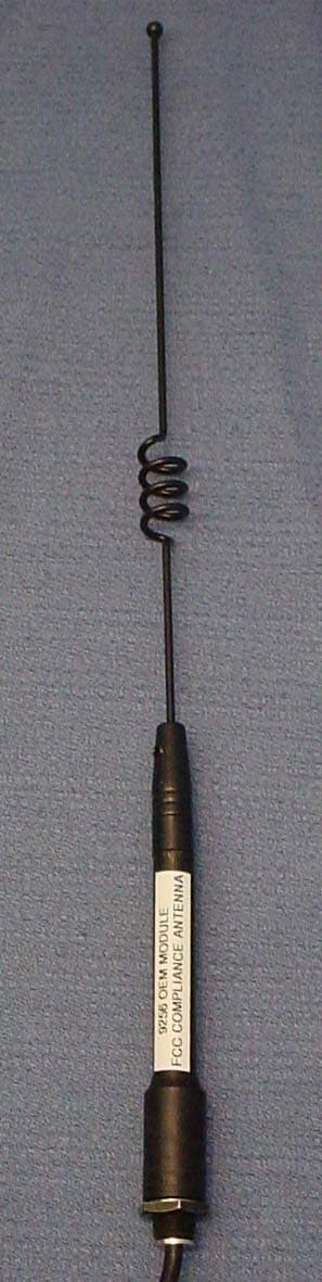
Click to zoom
Application Details
- Equipment Class
- DSS - Part 15 Spread Spectrum Transmitter
- Date of Grant
- Aug 31, 2004
- Application Purpose
- Original Equipment
- Date of Application
- Aug 31, 2004
- Equipment Note
- Radio Modem Module
- Frequency Range
- 902.00000000 - 928.00000000
- Company
- STI Engineering Pty Ltd
- Country
- Australia
Documents & Files
Document Text
Text extracted from the exhibit documents filed with the FCC. Open a document above to read the original.
Users Manual
RFI-9256 RADIO MODEM USER MANUAL RFI-9256 Radio Modem User Manual DISCLAIMER © 2004 RF Innovations Pty Ltd. All rights reserved. RF Innovations reserves the right to make improvements on the product in this manual at any time without notice. No part of this manual may be produced, copied, translated, or transmitted in any form or by any means without the written permission of RF Innovations. Information provided in this manual is intended to be accurate and reliable. However, RF Innovations assumes no responsibility for its use or infringements upon the rights of third parties that may result from its use. FCC NOTIFICATIONS This device must be operated as supplied by RF Innovations. Any changes or modifications made to the device without the express written approval of RF Innovations may void the user's authority to operate the device. This device complies with Part 15 of the FCC rules. Operation is subject to the following two conditions: 1) this device may not cause harmful interference and 2) this device must accept any interference received, including interference that may cause undesired operation. This equipment has been tested and found to comply with the limits for a Class B digital device, pursuant to Part 15 of the FCC Rules. These limits are designed to provide reasonable protection against harmful interference in a residential installation. This equipment generates, uses and can radiate radio frequency energy and, if not installed and used in accordance with the instructions, may cause harmful interference to radio communications. However, there is no guarantee that interference will not occur in a particular installation. If this equipment does cause harmful interference to radio or television reception, which can be determined by turning the equipment off and on, the user is encouraged to try to correct the interference by one or more of the following measures: ∑ Reorient or relocate the receiving antenna. ∑ Increase the separation between the equipment and receiver. ∑ Connect the equipment into an outlet on a circuit different from that to which the receiver is connected. ∑ Consult the dealer or an experienced radio/TV technician for help. Reference No. MAN0005 Revision 3.6 August 2004 Contents RFI-9256 Radio Modem User Manual Page 3 of 96 Contents 1. Introduction ............................................................................................................................................................................. 5 1.1 OEM Applications ............................................................................................................................................................ 5 1.2 Product Overview............................................................................................................................................................. 5 2. Installation................................................................................................................................................................................ 6 2.1 Radio Frequency Hazard Information ............................................................................................................................. 6 2.2 RFI-9256 Location ........................................................................................................................................................... 6 2.3 Antenna Installation ......................................................................................................................................................... 6 3. Configuration ........................................................................................................................................................................... 7 3.1 User Interfaces ................................................................................................................................................................. 7 3.2 Terminal Menu Interface.................................................................................................................................................. 7 3.3 Hayes AT Command Interface ......................................................................................................................................... 8 3.4 Front Panel Interface ..................................................................................................................................................... 10 4. Operation................................................................................................................................................................................ 14 4.1 Serial Port Operation..................................................................................................................................................... 14 4.2 Radio Operation............................................................................................................................................................. 17 4.3 Protocol Operation ........................................................................................................................................................ 26 4.4 Auxiliary I/O................................................................................................................................................................... 27 5. Applications............................................................................................................................................................................ 27 5.1 Basic Point-to-point Network ......................................................................................................................................... 27 5.2 Simplex Point-to-point Network ..................................................................................................................................... 27 5.3 Multiple Slave Point-to-point Network..............................…
Text truncated - open the document above for the full version.
Cover Letter(s)
-ABN 97 065 523 579- 22 Boulder Rd Malaga W.A. 6090 PH. (08) 9209 0900 FAX (08) 9248 2833 www.rfinnovations.com.au Wednesday, August 11, 2004 TO: Federal Communications Commission (FCC) Laboratory Division 7435 Oakland Mills Road Columbia, MD 21046 USA Dear Sir/Madam, CONFIDENTIALITY REQUEST Reference rule sections 0.457 (d) (ii) and pursuant to rule section 0.459 (a) confidentiality is requested as follows. Specific Information: Schematics diagrams, Layout diagrams, Bill of materials (BOM) This information contains trade secret information that is not routinely made available. Disclosure of this information could result in an unfair advantage to our competitors. It should be treated as confidential for the duration of the Grant Of Authorisation. This letter formally requests the withholding from public disclosure proprietary information submitted pursuant to an Application for Equipment Authorisation, FCC ID: P5M9256OEM. Our FCC Registration Number (FRN) is 0011306867. Best regards, Carlos M. Tomaz Engineering Manager, RF Innovations.
Cover Letter(s)
Response to TCB Findings 11.20dB bandwidth of 255kHz is higher than the declared channel separation of 250kHz. According to 15.247(a)(1), frequency hopping systems shall have hopping channel carrier frequencies separated by a minimum of 25kHz or the 20dB bandwidth of the hopping channel, whichever is higher. How does the device comply with this requirement? Please clarify. Please refer the document labelled RFI TCB response. The 20 dB bandwidth has been remeasured at being less than 250 kHz. As a result the device utilises a minimum of 50 channels. 12. Please clarify what was meant with ">-41dBm" for out of band conducted emissions on Pg 20 and 21 of the report. With reference pages 20 and 21, all spurious emissions observed from the device were greater than 20 dB of the limit however for completeness for my client I have recorded the levels that I observed. At 1800 MHz, being 2 * fc it was difficult to record a level that was not causing the spectrum analyser to be overloaded. So -41 dBm was the level recorded where the emission could no longer be observed indicating that the emission had a true value being less than -41 dB. One attenutator step back the level was still not a true level as the analyser was still be overloaded. 13. For radiated emissions above 1GHz, have peak levels of the emissions (with 1MHz RBW and VBW) complied with 74dBuV/m limit (20dB above average)? Also the data tables have no readings on them, does this mean no emissions have been recorded? What was the noise floor of the measurement system? Please clarify. Emission measurements were initially made at a distance of 3 metres with no spurious emissions being detected. Additional measurements were made at a closer distance of approximately 1 metre with no emissions also being detected. Measurements were made in average with checks also made in peak but no emissions were detected in this mode. Between 1 - 9 GHz a noise floor starting at approximately 25 dBuV/m working its way up to approximately 44 dBuV/m was observed. Moving into a distance of 1 metre allowed the margin to the limit to be increased by an additional 10 dB which allowed a 20 dB margin to the limit. 14. The radiated emissions test set-up photos does not show the antenna connected to the device as seen in AC line conducted emissions test set-up photo. Was the antenna connected to the board during radiated emissions test? Has the antenna position of the device been varied in all possible orthogonal orientations to maximize the emissions? Please clarify. Emission measurements were made in two modes. - with the antenna terminal terminated with a dummy load - with an antenna attached The photographs have been taken with the dummy load attached. The results obtained were identical. When the antenna was attached to the device the antenna was placed in a vertical postion and it was rotated using the turntable and the polarisation of the receiving antenna was changed between vertical and horizontal. This process was also carried out when the dummy load was attached. 15. Please supply EIRP readings calculated from the fundamental field strength reading of the emission (on 3 channels). This is needed to verify that the measured EIRP complies with the 36dBm limit. The maximum power output of the device and the antenna gain give a theoretical radiated power output of 34.9 dBm. The limit is 36 dBm. Using the antenna described in the report the following radiated power measurements were determined: The worst case power level determined was 31.9 dBm. Details of these measurements are contained within a file labelled radiated power. 16. Please confirm that a 50ohm/50uH LISN has been used for AC line conducted emissions test. A Rohde and Schwarz ESH2-Z5 Artifical mains network was used to make AC line conducted emission measurements. This is a 50 ohm / 50 mirohenry mains network.
Cover Letter(s)
RF Innovations Pty Ltd Report on FCC Compliance RD0565 Rev 4.1 Page 18 of 38 04-08-23 4 TCB SUBMISSION This section addresses points specifically requested by EMCT upon submission to TCB selected by EMCT (Curtis- Strauss). The TCB requested clarifications are pasted in italic. Refer to [16] as well as exchange of correspondence in Section 5 below. Equipment used: • Spectrum analyser: Agilent ESA E4407B • Oscilloscope: Agilent 54642A • RF Signal generator: Agilent E4437B 4.1 PCB Overlays. 1. Layout diagrams have been mentioned in the confidentiality request. This document was not supplied. Please provide the document or revise the confidentiality request. Please refer to CD Rev 1.0.3, under the directory “/PCB Overlays”. 4.2 Operational Description 2. An operational description is required as a separate exhibit. If this is part of the manual, it needs to be extracted and supplied. This description should also address the following issues; The mentioned issues are dealt with separately below. 4.2.1 Pseudo-random hopping sequences a. Is the hopping sequence pseudorandom? Provide examples of the hopping sequence. The hopping pattern sequences are pseudo-random. Hopping pattern sequences are calculated using a linear congruential generator, of the form [11]: () mbayy nn mod 1 += + The MINSTD generator is used, having constants: 0 168077 214748364712 5 31 = == =−= b a m The procedure for generating the 32 hopping patterns is as follows. 1. Set y 0 = 389. RF Innovations Pty Ltd Report on FCC Compliance RD0565 Rev 4.1 Page 19 of 38 04-08-23 2. Generate the first hopping pattern channel c 1 by calculating (y 1 mod MAX_CHANNELS 3 ). 3. Generate the n th hopping pattern channel by calculating (y n mod MAX_CHANNELS). If this is the same as any of the channels c 1 to c n-1 already in the sequence, discard the result and use (y n+1 mod MAX_CHANNELS) instead. Repeater until a valid hopping pattern channel is found. 4. Repeat step 3 until such time as a full hopping pattern is generated. 5. Repeat steps 2, 3, and 4 until each hopping pattern is generated. An example of different hopping patterns is provided in Table 12 below [12]. HSN stands for “Hopping Sequence Number”. The slot number corresponds to the FCC channel number visited in successive time slots. HSN [0..31] Slot Number [0..101] 0 29, 98, 26, 30, 17, 99, 36, 64, 79, 74, 13, 9, 85, 57, 61, 89, 8, 81, 69, 96, 75, 14, 6, 33, 15, 22, 34, 95, 45, 23, 2, 35, 32, 83, 41, 78, 90, 43, 12, 87, 53, 21, 3, 80, 48, 40, 7, 91, 42, 16, 1, 54, 38, 44, 18, 73, 20, 71, 62, 101, 11, 52, 39, 47, 82, 4, 58, 97, 46, 56, 60, 55, 50, 25, 37, 77, 19, 94, 70, 67, 88, 76, 0, 27, 24, 100, 5, 93, 49, 68, 72, 31, 92, 65, 63, 86, 66, 51, 28, 59, 10, 84 16 81, 90, 31, 77, 100, 70, 86, 53, 68, 3, 62, 58, 41, 92, 1, 28, 61, 46, 101, 79, 20, 4, 60, 91, 24, 93, 87, 12, 35, 40, 57, 73, 19, 48, 27, 6, 69, 95, 7, 74, 36, 49, 55, 5, 33, 59, 54, 30, 51, 82, 42, 25, 85, 29, 56, 64, 45, 8, 17, 2, 34, 80, 38, 22, 63, 52, 71, 13, 65, 83, 32, 78, 10, 76, 18, 9, 66, 88, 67, 75, 89, 37, 47, 96, 50, 98, 0, 26, 16, 84, 44, 14, 15, 99, 43, 94, 21, 39, 72, 11, 97, 23 31 96, 55, 25, 100, 95, 64, 91, 12, 40, 97, 10, 17, 45, 31, 81, 101, 51, 65, 73, 47, 6, 79, 82, 61, 59, 36, 20, 77, 88, 34, 14, 4, 50, 15, 84, 44, 76, 32, 43, 46, 52, 74, 18, 66, 86, 70, 68, 71, 22, 42, 67, 63, 75, 8, 94, 16, 1, 7, 69, 2, 53, 99, 62, 19, 85, 28, 54, 23, 48, 29, 3, 58, 38, 0, 90, 78, 39, 5, 24, 37, 21, 57, 41, 9, 98, 72, 93, 27, 92, 49, 33, 60, 35, 30, 26, 11, 13, 56, 89, 80, 83, 87 Table 12: Example FCC hopping patterns In addition to the standard 32 hopping patterns, three additional patterns are supplied that are only available in factory mode, as shown in Table 13 below. These patterns cannot be used to link or transfer data, they are only used for the purpose of testing the VCO range. HPSN Description 32 Hops between channels 0 and 100 only. 33 Only hops over the lower 50% of the band. 34 Only hops over the higher 50% of the band. Table 13: Factory mode hopping patterns 4.2.2 Equi-probable channels b. How is the equal use of each channel on average ensured by the device? 3 MAX_CHANNELS = 102, for the FCC image. RF Innovations Pty Ltd Report on FCC Compliance RD0565 Rev 4.1 Page 20 of 38 04-08-23 The method for generating the hopping sequence described in 4.2.1 ensures that within each hopping sequence, each of the 102 channels occurs once. Under normal operation the hopping sequence is cycled i.e. after the EUT has dwelled on the last channel in the sequence it will then hop back to the first and then hop through the sequence ad infinitum. Therefore each channel is visited once every 102 channels. The frame time is the amount of time that the RFI-9256 will spend on each channel in the hopping pattern. This is also referred to as the channel dwell time. [9] The frame time is user-configurable, 5ms to 35ms [9] with the one setting being applied to all the channels in the hopping sequence. Therefore equal use of all channels is guaranteed. Some evidence for this is shown in the following figure. Figure 5 :Channel frequency tuning voltage In figure 5 the lower trace is the tuning voltage on the channel changing main VCO of the EUT measured at TP1 of the circuit. The upper trace is the TX/RX switch line measured at TP34 and was used to trigger the oscilloscope. The vertical time cursors show where the pattern repeats indicating the period for a complete 102 channel hopping sequence. 4.2.3 Compliant receiver bandwidth c. Does the associated system receiver have a compliant input bandwidth, based on the measured 20 dB emission bandwidth? The RFI-9256 OEM module receiver bandwidth is determined by its last (2 nd ) IF (10.7MHz). The IF filter used is Murata SFELA10M7JAA0-B0. Refer to filter characteristics in Figure 6 below. As can be seen, the filter bandwidth comfortably fits within the declared 20dB channel bandwidth (250KHz). RF Innovations Pty Ltd Report on FCC Compliance RD0565 Rev 4.1 Page 21 of 38 04-08-23 Fig…
Text truncated - open the document above for the full version.
Cover Letter(s)
9. Answers to the FCC part 15 section 15.247 Clause (f): The RFI-9256 OEM module is not a hybrid system, within the context of clause (f). It operates in frequency-hopping mode, with the baseband signal being GMSK modulated. No spreading code is used on the baseband signal prior to frequency-hopping. Clause (g): The RFI-9256 OEM operates in fixed frames, Time-Division Duplex mode. It is thus not designed to operate in continuous transmission mode. The selected frame time is the channel dwell time. All channels are equiprobable. Clause (h): The RFI-9256 OEM does not provide multi-user detection for the purpose of channel avoidance, such as adaptive frequency hopping patterns with e.g. channel exclusion. Blocked channels may result in loss of data. The lost data is repeated via ARQ. The RFI-9256 operates in a master/slave mode. Masters transmit according to the selected hopping sequence number. Frequency-hopping of co-located masters is pseudo-random in nature and is not coordinated in a manner to select mutually exclusive channels.
External Photos
EMC Technologies (NZ) Ltd Test Report No 40616.1 Report date: 29 July 2004 EMC Technologies (NZ) Ltd Telephone: +64 9 360 0862 Fax: +64 9 360 0861 STREET ADDRESS - 47 MacKelvie Street, Grey Lynn, Auckland, New Zealand E-mail: [email protected] POSTAL ADDRESS - PO Box 68 307, Newton, Auckland, New Zealand Web Site: www.emctech.com.au This report may not be reproduced except in full Page 30 of 30 Antenna
ID Label/Location Info
EMC Technologies (NZ) Ltd Test Report No 40616.1 Report date: 29 July 2004 EMC Technologies (NZ) Ltd Telephone: +64 9 360 0862 Fax: +64 9 360 0861 STREET ADDRESS - 47 MacKelvie Street, Grey Lynn, Auckland, New Zealand E-mail: [email protected] POSTAL ADDRESS - PO Box 68 307, Newton, Auckland, New Zealand Web Site: www.emctech.com.au This report may not be reproduced except in full Page 27 of 30 Label details
Internal Photos
Top of the circuit board showing with the can removed. Top of the device with the can attached. Rear of the board ear of the board. The other end. Top of the board with the case attached. Complete device rear Complete device top with the label attached
Operational Description
RF Innovations Pty Ltd Report on FCC Compliance RD0565 Rev 4.2 Page 18 of 44 04-08-26 4 TCB SUBMISSION This section addresses points specifically requested by EMCT upon submission to TCB selected by EMCT (Curtis- Strauss). The TCB requested clarifications are pasted in italic. Refer to [17] as well as exchange of correspondence in Section 5 below. Equipment used: ∑ Spectrum analyser: Agilent ESA E4407B ∑ Oscilloscope: Agilent 54642A ∑ RF Signal generator: Agilent E4437B 4.1 PCB Overlays. 1. Layout diagrams have been mentioned in the confidentiality request. This document was not supplied. Please provide the document or revise the confidentiality request. Please refer to CD Rev 1.0.3, under the directory “/PCB Overlays”. An updated letter has been provided where confidentiality is only requested for schematics and BOM. Overlays have been removed from the exhibit. It was left out to EMCT on how to deal with this issue. 4.2 Operational Description 2. An operational description is required as a separate exhibit. If this is part of the manual, it needs to be extracted and supplied. This description should also address the following issues; The mentioned issues are dealt with separately below. 4.2.1 Extracts of Operational Description From [9]: The RFI-9256 is a frequency-hopping spread spectrum (FHSS) radio modem operating in the international 900MHz ISM band. It has been type approved for operation in Australia (915-928MHz), New Zealand (921-929MHz), and countries regulated by the FCC (902-928MHz). The RFI-9256 is suitable for many applications including point-to-point, point-to-multipoint, and SCADA protocol networks. An RFI-9256 OEM module is available for OEM applications. It incorporates the following features [9]: ∑ CRC error detection and recovery via retries ∑ Up to 30km point-to-point ∑ Dual RS-232 serial ports ∑ User selectable interface speeds between 110 and 115200bps ∑ 1 W (30dBm) RF output power RF Innovations Pty Ltd Report on FCC Compliance RD0565 Rev 4.2 Page 19 of 44 04-08-26 ∑ Programmable I/O for SCADA applications ∑ Front panel indicators for RSSI, TX power, and status ∑ Can be installed and commissioned without test equipment. ∑ Sensitivity <-108dBm for BER 1 part in 10-4 ∑ Operating voltage 9 to 30VDC ∑ Operates at -10ºC to +60ºC with 95% non-condensing humidity ∑ Protocol routing modes. Its applications are briefly described [10]: ∑ Point to Multipoint Data Acquisition and Control Intelligent built in Modem can interface with virtually any standard Data logger, PLC, computer; i.e. any RS232device. In built buffers handshake with Input/output devices at data speeds up to 115,000 bps and transparently move data to the other end. ∑ Linking of local and remote RS232 serial ports Depending upon the geography and terrain, the Radio modems can communicate reliably over considerable distances. Good line of site paths from mountain top to hill can extend useful range up to 30 km. The RFI 9256 can be used as a repeater to extend range indefinitely. ∑ Parallel digital I/O and expansion 8 parallel digital I/O in addition to the standard RS232 serial port, are provided in the RFI 9256 model Radio modems. Expansion radio interface modules (RIM) permit very large SCADA capability. For more details regarding interface parameters, contact the manufacturer. ∑ Diagnostics functions The second RS 232 port can be used as a diagnostics channel for monitoring network performance, and for additional data routing if required. A low-level RF transceiver block diagram is provided Figure 1 below, for reference purposes: TX/RX BP PA PLL BPBP IF PLL SAW 915MHz SAW 915MHz LNA LO1 224.7MHz 10.7MHz 700MHz 214MHz BP SAW 915MHz MOD IN MOD OUT LO2 OSC 14.75MHz Figure 1: RFI-9256 RF Transceiver Block Diagram
Operational Description
RF Innovations Pty Ltd Report on FCC Compliance RD0565 Rev 4.2 Page 24 of 44 04-08-26 Please refer to CD Rev 1.0.3, under the directory “/Pictures/Detailed Views”, for pictures of OEM Module inside the case: ∑ “DSCF0017.jpg” shows the OEM module inside its case, with the bottom cover removed; ∑ “DSCF0001.jpg” shows the top view of the radio modem. The LEDs and pushbutton can be seen in this view. Refer to User Manual [9] for detailed description of user interface; ∑ “DSCF0010.jpg” is a front detail of the RF connector, with the FCC connector fitted; ∑ “DSCF0011.jpg” is a side detail of the RF connector; ∑ “DSCF0002.jpg” shows a detail of the DB-25 connector. 4.4 Transmitter views 4. Please supply closer and more detailed views of the transmitter board. Both sides with and without shields are required. The components must be clearly visible. Please refer to CD Rev 1.0.3, under the directory “/Pictures/Detailed Views”, for detailed views of the transmitter section: ∑ “9256 OEM Top.jpg”: Whole view of the top (primary or component side) of the module, showing the IDC connected, for illustration purposes only. ∑ “9256 OEM Bottom.jpg”: Whole view of the bottom (secondary or solder side) of the module, showing the IDC connected, for illustration purposes only. ∑ “9256 OEM Top detail 2.jpg”: Top view of the top (primary or component side) of the module, with focus on the RF section. Shown with OEM and VCO cans removed. ∑ “9256 OEM Bottom detail 2.jpg”: Bottom (secondary or solder side) view of the module, with focus on transmitter ground plane: ∑ “9256 OEM can1.jpg”: Top view of the top (primary or component side) of the module, with OEM can removed. VCO can is shown. Tabs on top of VCO can connect to OEM can. ∑ “9256 OEM TX strip.jpg”: Detailed view of the transmitter section of the RF transceiver. The VCO canned section has been removed for the sake of clarity. 4.5 Antenna connector specifications 5. Please supply the specifications of the antenna connector on the board. Please refer to CD Rev 1.0.3, under the directory “/BNC Connector”, for detailed views of the transmitter section: ∑ “FCC_FERRULE.PDF” is the mechanical drawing for the ferrule and contains all required specifications for its manufacture; ∑ “FCC_BNC_CONNECTOR.PDF “is the mechanical drawing for the matching BNC connector and also contains all required specifications for its manufacture. The transmitter is fitted with a standard right-angle shielded PCB-mount female BNC connector. This connector is modified by way of fitting a shroud over its mating end (refer to “FCC_FERRULE.PDF”). The shroud is then screwed on and permanent secured with thread locking adhesive (Loctite). There are no provisions for gripping facilities on the shroud, thus separation of the two parts is near impossible. This modification turns a “standard BNC” connector into a non-standard “unique BNC” connector. The shroud fitted over the transmitter board connector limits the diameter of a connector that this connector can accept, thus a “BNC connector” with a smaller overall diameter is required. A non-modified (standard) BNC antenna cable connector can not be connected to the transmitter board. The supplied antenna coaxial cable is fitted with a modified male BNC (modified connector as shown in “FCC_BNC_CONNECTOR.PDF”), which allows mating of the two connectors: transmitter and antenna. 4.6 Label 6. Please specify the label material and supply a placement photo on the device.
Operational Description
www.rfindustries.com.au R-62 Cellular Elevated Feed Antennas 825-960 MHz CD1225 Series 3.0 dB - CDMA CD1625 Series 3.0 dB - GSM CD1228 Series 3.0 dB - Fender Mount - CDMA CD1628 Series 3.0 dB - Fender Mount - GSM CD1250 Series 5.0 dB - CDMA Elevated Feed Antennas - these ‘problem solvers’ provide high performance in virtually any mounting position. The elevated feed design raises the radiating element above the vehicle roof level to provide a strong omnidirectional pattern and high performance for vehicle gutter, fender, boot or magnetic mounting. The whip and air wound phasing coil are constructed from a single piece of precipitation hardened stainlesss steel finished in sytlish black plating. The elevated feed section is hand crafted from brass and finished with a black chrome plating. •High performance omnidirectional gain •‘Problem Solver’ - Elevated feed design eliminates need for a ground plane and boosts the radiating element over obstructions •Black finish will not scratch or peel •Limited lifetime warranty CDMA - 825-896 MHz GSM - 890-960 MHz 3.0 dB Elevated Feed Antennas •3.0dB omni-directional gain elevated feed design eliminates need for ground plane •Various mounting kits available 5.0 dB Elevated Feed Antennas (CDMA only) •Designed primarily for country areas or fringe area locations •High Performance - 5.0 dB omni-directional gain •Elevated feed design eliminates need for ground plane •Various mounting kits available CD1625 CD1250 FK-851 www.rfindustries.com.au R- 63 Cellular Elevated Feed Antennas 825-960 MHz CD1225 Series CD1625 Series CD1228 Series CD1628 Series CD1250 Series TEST FREQUENCY: 850 MHz REFERENCE ANTENNA MODEL: SW1405 MOUNT: MB14 POSITION: Roof Centre TEST ANTENNA MODEL: CD1225 MOUNT: Guttermount POSITION: Gutter Passenger Side This pattern clearly shows that when mounted on the gutter clear of obstructions, this antenna is providing a gain of 4.5dB or more over a 1/4 wave whip and a pattern variance of only 1-2dB. The antenna is clearly operating independent of the ground plane and is a superior choice in this mounting position. Electrical .oNledoM niaG )Bd( ycneuqerF )zHM( rewoP )sttaW( gninuT seireS5221DC 0.3 698-528 05 ,denut-erpdeilppuS noitallatsnirofydaer seireS5261DC 069-098 seireS8221DC 0.3 698-528 seireS8261DC 069-098 seireS0521DC 0.5698-528 Mechanical 30° 0° 60° 90° 120° 150° 330° 300° 270° 240° 210° 180° 0 5 10 20 25 30 35 15 .oNledoMlairetaMpihW htgneLpihW )mm( detsegguS gnitnuoM dnaelbaC rotcennoC seireS5221DC ,leetssselniatShP7-71 hsinifkcalb 074 dutSmm41 m0.5htiwdeilppuS .elbac®maoflleC ,FHUiniMyficepS roEMF,elam-AMS srotcennocelam-N seireS5261DC 234 seireS8221DC 595 redneF158-KF tnuom seireS8261DC 755 seireS0521DC 567dutSmm41
RF Exposure Info
EMC Technologies (NZ) Ltd Test Report No 40616.1 Report date: 29 July 2004 EMC Technologies (NZ) Ltd Telephone: +64 9 360 0862 Fax: +64 9 360 0861 STREET ADDRESS - 47 MacKelvie Street, Grey Lynn, Auckland, New Zealand E-mail: [email protected] POSTAL ADDRESS - PO Box 68 307, Newton, Auckland, New Zealand Web Site: www.emctech.com.au This report may not be reproduced except in full Page 19 of 30 Section 15.247 (b) (5) – Radio Frequency Hazard Information As per Section 15.247 (b) (4) spread spectrum transmitters operating in the 902 – 928 MHz band are required to be operated in a manner that ensures that the public is not exposed to rf energy levels in accordance with CFR 47, Section 1.1307(b)(1). In accordance with this section, and also Section 2.1091, this device has been defined as a mobile device whereby a distance of 20 cm can normally be maintained between the user and the device. In accordance with Section 1.1310 the Maximum Permissible Exposure (MPE) limits for the General Population / Uncon…
Text truncated - open the document above for the full version.
Contact Information
Applicant
Johan Svean(Managing Director)
Test Firm
EMC Technologies NZ Ltd.Andrew Cutler
Technical Specifications
| # | Rule Parts | Frequency Range | Power Output |
|---|---|---|---|
| 1 | 15C | 902 MHz - 928 MHz | 932.00 mW |
Other Applications from STI Engineering Pty Ltd
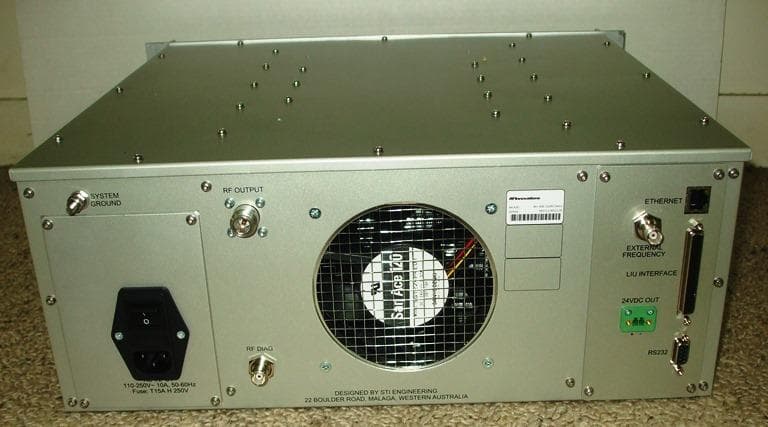
P5MRFI400
Aug 07, 2023RFI-400 250W UHF Paging Transmitter
Equipment Class
TNB - Licensed Non-Broadcast Station Transmitter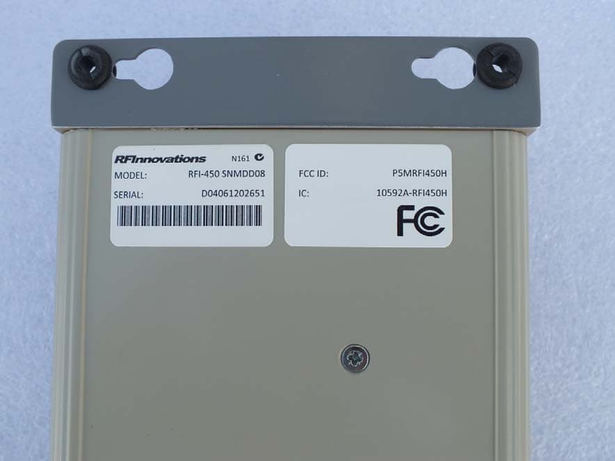
P5MRFI450H
Nov 05, 2013UHF DIGITAL MOBILE RADIO
Equipment Class
TNB - Licensed Non-Broadcast Station Transmitter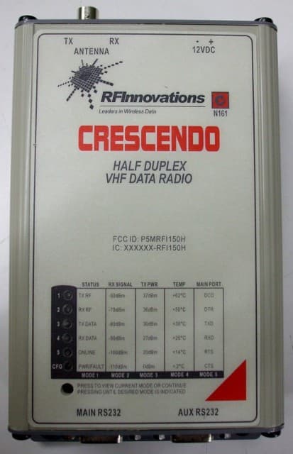
P5MRFI150H
Dec 18, 2012VHF Digital Mobile Radio
Equipment Class
TNB - Licensed Non-Broadcast Station Transmitter
P5M9256TRX
Apr 02, 2002Frequency Hopping Spread Spectrum Transceiver
Equipment Class
DSS - Part 15 Spread Spectrum Transmitter