P6T1903Bidirectional Amplifier
P.G.Electronics Ltd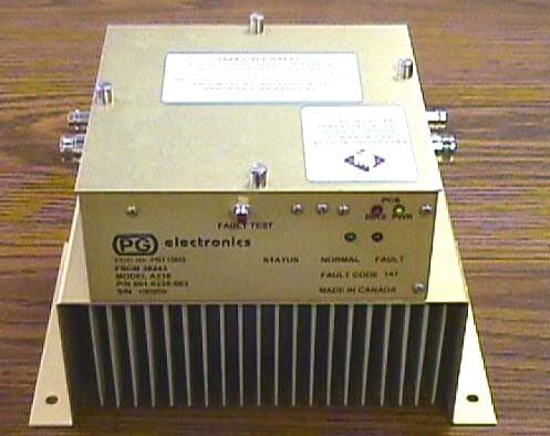
Click to zoom
Application Details
- Equipment Class
- AMP - Amplifier
- Date of Grant
- Nov 28, 2004
- Application Purpose
- Original Equipment
- Date of Application
- Sep 06, 2004
- Equipment Note
- Bidirectional Amplifier
- Frequency Range
- 1930.00000000 - 1990.00000000
- Company
- P.G.Electronics Ltd
- Country
- Canada
Documents & Files
Document Text
Text extracted from the exhibit documents filed with the FCC. Open a document above to read the original.
Users Manual
P. G. TM0060 electroni cs electronics OPERATOR'S MANUAL PCS BIDIRECTIONAL AMPLIFIER MODEL A238 P/N 001-0238-003 (LOCAL POWERED ) AUGUST 2004 RESTRICTION ON DISCLOSURE OF DATA This document contains information proprietary to P.G. Electronics and any disclosure or use of this information or any reproduction of this document for other than the specific purpose for which it is intended is expressly prohibited except as P.G. Electronics may otherwise agree in writing. REV. 0 Weston, Ontario P. G. TM0060 GUARANTEE This unit is guaranteed for a period of one year from the date of shipment against failure due to defective parts or improper assembly. This guarantee is limited to replacement of defective material and does not cover damages or other costs resulting from the use of this material whether used correctly or otherwise. P. G. TM0060 i TABLE OF CONTENTS Paragraph Page SECTION 1. GENERAL INFORMATION 1.1 INTRODUCTION 1-1 1.1.1 Scope of Manual 1-1 1.1.2 Purpose of Equipment 1-1 1.1.3 Physical Description 1-1 1.1.4 Electrical Description 1-1 1.2 TECHNICAL SUMMARY 1-2 SECTION 2. THEORY OF OPERATION 2.0 GENERAL 2-1 2.1 DESCRIPTION 2-1 2.2 FAULT REPORTING 2-3 2.2.1 General 2-3 2.2.2 Report Type 2-3 2.2.3 Fault Conditions 2-4 SECTION 3. INSTALLATION, OPERATING AND MAINTENANCE INSTRUCTIONS 3.1 UNPACKING AND INSPECTION 3-1 3.2 INSTALLATION 3-2 3.3 OPERATING INSTRUCTIONS 3-4 3.4 FAULT CONDITIONS 3-4 SECTION 4. PROGRAMMING OPTIONS 4.0 PROGRAMMING OPTIONS 4-1 4.1 DC CONTINUITY 4-1 4.2 ATTENUATION 4-2 4.3 FAULT OPTIONS 4-2 4.4 STATUS OPTIONS 4-4 4.5 TEST 4-4 4.6 FAULT CODE 4-4 P. G. TM0060 ii LIST OF FIGURES Figure Title Page 2-1 A238 BIDIRECTIONAL AMPLIFIER - BLOCK DIAGRAM 2-2 3-1 INSTALLATION DATA 3-3 4-1 A238 PROGRAMMING OPTIONS – JUMPER LOCATIONS 4-3 4-2 FAULT CODE SETTING EXAMPLES 4-5 A-1 AUTOSET SHUNT POSITIONS A-3 LIST OF TABLES Table Title Page 1-1 PERFORMANCE CHARACTERISTICS AND SALIENT 1-2 FEATURES OF THE A238 PCS BIDIRECTIONAL AMPLIFIER 1-2 RATED POWER OUTPUT FOR LINEAR OPERATION 1-3 A-1 A238 SHUNT INSTALLATION A-4 APPENDIX A A AUTOSET ATTENUATION OPTION (IF INSTALLED) A-1 A-1 GENERAL A-2 A-2 INSTALLATION A-2 A-3 OPERATION A-2 P. G. TM0060 1-1 SECTION 1. GENERAL INFORMATION 1.1 INTRODUCTION 1.1.1 Scope of Manual - This manual is intended to familiarize service personnel working on the PCS Bidirectional Amplifier A238 with all pertinent aspects of the amplifier. Included in this manual are a brief physical description, a technical summary, installation information and operating data. 1.1.2 Purpose of Equipment - The A238 amplifier is used as a drop-in booster for PCS signals. It will simultaneously amplify signals in the PCS transmit band in one direction and the PCS receive band in the opposite direction. A typical use of the A238 is to provide wireless phone coverage in underground installations. 1.1.3 Physical Description - The bidirectional amplifier, shown in Figure 3-1, is designed to be mounted on a flat vertical surface. The unit has two N connectors for external electrical connection and two BNC test ports to check RF signals. Color coded indicators provide visual display of the unit's operating status. 1.1.4 Electrical Description - The bidirectional amplifier provides approximately 20 dB of gain for signals in the 1850 - 1910 MHz band in the direction of J1 to J2 (antenna to base) and the same amount of gain for signals in the 1930 - 1990 MHz band in the opposite direction (J2 to J1). 1.1.4.1 The unit is locally powered through a 5-pin DIN receptacle. The P.G. Electronics PS293 power source should be used to power the unit. The unit provides DC continuity from J1 to J2 to allow powering of downstream amplifiers from upstream power sources such as PS212 and PS213. Local power is isolated from J1 and J2. 1.1.4.2 The unit monitors bias conditions of active devices in the RF path and monitors downlink power. If one of these devices draws more or less than a predetermined limit, or if the RF downlink power is low then the FAULT indicator will go on. Under normal operating condition only the green NORMAL indicator will be on. 1.1.4.3 If a FAULT condition is detected the unit transmits a low frequency identification code along the cable center conductor. The burst transmission is repeated at approximately 80 second intervals while a fault condition exists. 1.1.4.4 If a NORMAL condition exists in the amplifier a low frequency OK identification code will be transmitted on the cable at intervals of approximately 80 minutes. 1.1.4.5 The unit has an adjustable attenuator to allow operation at reduced gain. The attenuator is settable in 1 dB steps up to 15 dB either manually or by using an optional AUTOSET control board. P. G. TM0060 1-2 1.2 TECHNICAL SUMMARY TABLE 1-1. Performance Characteristics and Salient Features of the A238 PCS Bidirectional Amplifier Parameter Specification 1. Input Power: 24 to 28 VDC @ 2 A Max (use PS 293) 2. Frequency Range*: Uplink: Downlink: 1850-1910 MHz 1930-1990 MHz 3. Gain: 20 dB ±2 dB 4. Impedance (Input and Output): 50 Ohms 5. VSWR: 2:1 Typical, 3:1 Maximum 6. Composite output power rating**: Uplink: Downlink: +4dBm +24dBm 7. 1dB Compression: Uplink: Downlink: +12 dBm +33 dBm 8. 3rd Order Output IP: Uplink: Downlink: +27 dBm +45 dBm 9. Attenuator Range 0 to 15 dB (1 dB steps) (optional Autoset PCB) 10. Environmental Limits: (a) Temperature Range: -30°C to 60°C operating (b) Relative Humidity: to 90% 11. Dimension and Weight: (a) Overall Dimensions: 9.8” L x 6.7” W x 6.7” H (b) Mounting Hole Dims: 9” x 5” (c) Weight: 5.8 lb (2.6 kg) 12. Connectors: RF Input/Output: Type N Female RF Test Input/Output: Type BNC Female DC supply: DC power jack *NOTE: Specifications apply only across the customer’s actual bands, not across the whole PCS spectrum. **NOTE: Refer to TABLE 1-2 for definition of composite output power rating. P. G. TM0060 1-3 NOTE IMPORTANT RATING INFORMATION Manufacturer’s rated output power of this equipment is for single carrier operation. For situa…
Text truncated - open the document above for the full version.
Cover Letter(s)
P. G. Electronics FCC ID: P6T1903 P6T1903CL1 P. G. Electronics 800 Arrow Road, Unit 8 Toronto, Ontario M9M 2Z8 Canada Sept. 2, 2004 Federal Communications Commission 7435 Oakland Mills Road Columbia, Maryland 21046 Ref.: P6T1903CL1 Dear Sir/Madame: RE: FCC ID: P6T1903 Attached is an application for Equipment Approval for our model A238 PCS bidirectional amplifier for the PCS band. The diplexers are fixed-tuned and the unit does not require any tuning. The unit contains no oscillator or frequency translation circuitry. The unit is similar to the A289 recently granted authorization by the FCC (FCC ID: P6T81902, Grant Date: June 21, 2002). The A238 is for PCS operation only while the A289 is for both cellular and PCS. The A238 is essentially the A289 with the cellular circuitry removed. The construction, components and rated output power of both units are the same. Installed units are used well within their linear operating region to provide low distortion and interference free systems. The unit is designed to be used for in-building signal enhancement. The unit allows operators to reduce interference problems by utilizing low power signals directed to the exact required coverage areas instead of using increased power at a distant antenna. The attached exhibits contain technical information to assist you in reviewing our application and test data which has been taken under my supervision. If you require any further information, please contact me and we will provide it immediately. Yours Sincerely, P. G. Electronics Ltd. Gerry Graham, P. Eng President ([email protected])
Cover Letter(s)
P. G. Electronics FCC ID: P6T1903 P6T1903CL2 P. G. Electronics 800 Arrow Road, Unit 8 Toronto, Ontario M9M 2Z8 Canada Sept. 2, 2004 Federal Communications Commission 7435 Oakland Mills Road Columbia, Maryland 21046 Ref.: P6T1903CL2 Dear Sir/Madame: RE: FCC ID: P6T1903 Request For Confidentiality P. G. Electronics requests confidentiality in accordance with FCC Regulations Section 0.459 for items submitted with the application for Type Approval of the R280P-DE (FCC ID: P6T1903). We request that the following exhibits be kept confidential: schematic, parts lists, and operational description. These items are considered as proprietary material and Trade Secrets. They are essential to the continuing successful business of P. G. Electronics. The references for these files are as follows: EXHIBIT FILENAME Schematic P6T1903SC.DOC Parts Lists P6T1903PL.DOC Operational Description P6T1903OD.DOC We appreciate your assistance in this matter. Yours Sincerely, P. G. Electronics Ltd. Gerry Graham, P. Eng President ([email protected])
Cover Letter(s)
P. G. Electronics 800 Arrow Road, Unit 8 Toronto, Ontario M9M 2Z8 Canada Sept. 14, 2004 Federal Communications Commission 7435 Oakland Mills Road Columbia, Maryland 21046 Ref.: P6T1903CL3 Re: FCC ID P6T1903, 731 Confirmation Number EA998317 Re: Correspondence Reference number: 27589 Re: FCC Identification Label Response: Please refer to the ID Label exhibit P6T1903ID and External Photos exhibit P6T1903EP. The ID label will appear as shown in the ID Label exhibit and will be located on the bottom of the unit as shown in the "A238 External View (Bottom)" photograph in P6T1903EP. And additional exhibit P6T1903LD has been submitted with this reply. It shows an enlarged photograph of the bottom of the unit. If any further detailed information is required, P. G. Electronics will provide this information as soon as possible. Sincerely. Gerry Graham P. G. Electronics
Cover Letter(s)
P. G. Electronics FCC ID: P6T1903 P6T1903CL4 P. G. Electronics 800 Arrow Road, Unit 8 Toronto, Ontario M9M 2Z8 Canada Nov. 9 2004 Federal Communications Commission 7435 Oakland Mills Road Columbia, Maryland 21046 Ref.: P6T1903CL4 Re: FCC ID P6T1903, 731 Confirmation Number EA998317 Re: Correspondence Reference number: 27983 Re: Active Devices Parts List Response: We have sent document P6T1903PL2 in response to the request for the list of active devices used. This parts list exhibit has been sent concurrently with this letter. We hope this addresses the requirement. If any further detailed information is required, P. G. Electronics will provide this information as soon as possible. Sincerely. Gerry Graham P. G. Electronics
External Photos
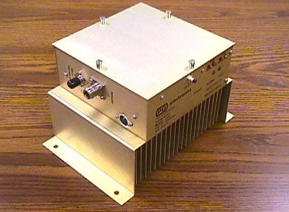
P. G. Electronics FCC ID: P6T1903 P6T1903EP Page 1 of 1 A238 EXTERNAL PHOTOS A238 EXTERNAL VIEW A238 EXTERNAL VIEW (BOTTOM)
ID Label/Location Info
P. G. Electronics FCC ID: P6T1903 P6T1903ID A238 FCC ID DRAWING PCS + + + + + + + + BIAS PWR FAULT TEST FCC ID: P6T1903 STATUS NORMAL FAULT FSCM 38243 MODEL A238 FAULT CODE P/N 001-0238-003 S/N MADE IN CANADA Note: Refer to external photos exhibit P6T1903EP for ID location on unit. electroni
ID Label/Location Info
P. G. Electronics FCC ID: P6T1903 P6T1903LD Page 1 of 1 A238 EXTERNAL PHOTO SHOWING ID LABEL POSITION DETAIL A238 EXTERNAL VIEW SHOWING LABEL DETAIL (BOTTOM VIEW)
Internal Photos
P. G. Electronics FCC ID: P6T1903 P6T1903IP Page 1 of 1 A238 INTERNAL PHOTOS PC BOARD ASSEMBLY HEATSINK ASSEMBLY
Parts List/Tune Up Info
P. G. Electronics FCC ID: P6T81903 P6T81903PL2 A238 ACTIVE DEVICE PART LIST TOP LEVEL REFERENCE PART NUMBER MANUFACTURER DESCRIPTION ITEM 3 MC7812ACT MOTOROLA POSITI VE VOLTAGE REGULATOR, 12V 1A MAIN AMPLIFIER BOARD ASSEMBLY REFERENCE PART NUMBER MANUFACTURER DESCRIPTION Q1,2 2N3904 MOTOROLA SMALL SIGNAL TRANSISTOR, NPN Q3 TIP30C MOTOROLA TRANSISTOR, PNP POWER U5 SGA-6389 SIRENZA INTEGR ATED CIRCUIT, RF AMP U6 SGA-7489 SIRENZA INTEGR ATED CIRCUIT, RF AMP U7 SGA-6289 SIRENZA INTEGR ATED CIRCUIT, RF AMP U10,12 LM393N NATIONAL SEMI IC DUAL COMPARATOR U13 LMC6062AIN NATIONAL SEMI IC DUAL OP AMP MDIP 8 PINS U14 LM1458N NATIONAL SEMI DUAL OP AMP U15 MC145026P MOTOROLA IC DATA ENCODER U16,17 AT-210-PIN M/A COM ATTENUATOR 1dB STEPS (LD) U20 CD4040BCM TEXAS INSTRUMENTS BINARY COUNTER U21,22 CD4093BCM TEXAS INSTRUMENTS DUAL NAND SCHMITT HEATSINK ASSEMBLY REFERENCE PART NUMBER MANUFACTURER DESCRIPTION U5,6 LM338T NATIONAL SEMI VOLT AGE REGULATOR ADJUSTABLE 5A U4 PA1166 M/A COM AMPLIFIER PCS
Test Report
P. G. Electronics FCC ID: P6T1903 P6T1903TR Page 1 of 27 TEST REPORT FOR FCC TYPE ACCEPTANCE MODEL A238 PCS BIDIRECTIONAL AMPLIFIER FCC ID: P6T1903 P. G. Electronics FCC ID: P6T1903 P6T1903TR Page 2 of 27 TEST REPORT P. G. Electronics, Ltd. is pleased to submit this technical report on tests performed on the Model A238 dual band bidirectional amplifier (FCC ID: P6T1903) to demonstrate compliance with the requirements for Type Acceptance by the FCC. The undersigned personnel verify that the tests were performed as described herein and the results given were measured on the production unit. Model Number A238 Serial Number 100955 ___________________________ Date ______________ Paul Liber – Test Engineer ___________________________ Date ______________ Gerry Graham – P. Eng. President P. G. Electronics FCC ID: P6T1903 P6T1903TR Page 3 of 27 1.0 NAMES AND ADDRESSES 1.1 Manufacturer The Model A238 bidirectional amplifier (FCC ID: P6T1903) is manufactured by: P. G. Electronics, Ltd. 800 Arrow Rd., Unit 8, Toronto, Ontario M9M 2Z8 Canada 1.2 Applicant The applicant for the acceptance of the amplifier is: P. G. Electronics, Ltd. 800 Arrow Rd., Unit 8, Toronto, Ontario M9M 2Z8 Canada P. G. Electronics FCC ID: P6T1903 P6T1903TR Page 4 of 27 2.0 COMPLIANCE The equipment has been tested in accordance with the following performance tests and the results provided below demonstrate compliance with FCC regulations. Please refer to section 3.0 for the list of test equipment used. Notes: For all tests, the D.U.T. internal attenuator has been set to 0 dB which makes the overall unit gain equal to 20 dB. The D.U.T. was locally powered from a PS293 24 VDC power source for all tests. 2.1 Gain The gain was measured using the test arrangement as shown in Figure 2.1-1 below. Measurements were made over typical customer's bands. Network Analyzer 1 Power Coupler D.U.T. Power Coupler 10 dB Attn. Power Supply (24 V) Figure 2.1-1 The unit gain was measured in both uplink and downlink directions. These results are shown in Plots 1 and 2 that follow. Plot 1 shows the uplink gain and Plot 2 shows the downlink gain. P. G. Electronics FCC ID: P6T1903 P6T1903TR Page 5 of 27 Plot 1: Uplink Gain Plot 2: Downlink Gain P. G. Electronics FCC ID: P6T1903 P6T1903TR Page 6 of 27 2.2 Intermodulation and Spurious Intermodulation and spurious products were measured with the amplifier operating at the maximum rated total inband power level as specified in the Operator's Manual. Three tone intermodulation tests were performed using the equipment test arrangement in Figure 2.2-1 below. Network Analyzer 2 Network Analyzer 1 Test Set Point A Combiner Power Coupler Driver Amp D.U.T. Power Coupler Terminator 10 dB Attn. Signal Generator Power Supply (24V) Point B Spectrum Analyzer *Notes: Model A211 driver amp was used for testing. Loss from Point A (D.U.T. output) to Point B (Spectrum Analyzer input) was 11.2 dB at PCS. This includes the loss of the 10 dB attenuator, Power Coupler and cables. Figure 2.2-1 P. G. Electronics FCC ID: P6T1903 P6T1903TR Page 7 of 27 A three tone test was performed on the unit in the uplink band with the input set to give the output power of –0.8 dBm for each uplink tone (+4 dBm maximum rated total inband power). The Network Analyzers were used as signal sources. The 11.2 dB loss to the spectrum analyzer results in tone levels of –12 dBm into the instrument. Plots 3, 4A and 4B show the results of the test. In Plot 3, the narrower sweep setting shows in- band intermodulation products, while in Plots 4A and 4B the spectrum outside the PCS band is displayed on a broad sweep to show harmonics and spurious. The spectrum analyzer reference level was set to –12 dBm. A three tone test was also performed in the downlink band with the input power levels adjusted to give the output power of +19.2 dBm for each downlink tone (+24 dBm maximum rated total inband power). The 11.2 dB loss to the spectrum analyzer results in tone levels of +8 dBm into the instrument. Plots 5, 6A and 6B show the results of the test for both narrow and broad sweeps with the spectrum analyzer reference level set to +8 dBm. P. G. Electronics FCC ID: P6T1903 P6T1903TR Page 8 of 27 Plot 4A: Uplink 3-tone Intermodulation (Sweep 0 – 2.9 GHz) Plot 3: Uplink 3-tone Intermodulation (Narrow Sweep) Plot 4B: Uplink 3-tone Intermodulation (Sweep 2.8 – 10 GHz) P. G. Electronics FCC ID: P6T1903 P6T1903TR Page 9 of 27 Examination of the above results shows that all products are more than 40 dB down. Plot 6A: Downlink 3-tone Intermodulation (Sweep 0 – 2.9 GHz) Plot 5: Downlink 3-tone Intermodulation (Narrow Sweep) Plot 6B: Downlink 3-tone Intermodulation (Sweep 2.8 – 10 GHz) P. G. Electronics FCC ID: P6T1903 P6T1903TR Page 10 of 27 2.3 Modulated Channel Tests These tests show a comparison of the input and output signals for operation with a single modulated signal at the maximum rated RF input drive level of the amplifier. Figure 2.3-1 below shows the test arrangement used for the tests. All the test results display the input level and the output level with sufficient attenuation to display it as an overlay on the same screen. Tests were performed for both the uplink and downlink directions. Tests were performed for each of NADC, GSM and CDMA modulations. The CDMA test signal was generated by using an external CDMA baseband modulation source connected to the signal generator as shown in the diagram. The CDMA baseband source was not connected to the signal generator for other modulation tests. The input signal is displayed on the spectrum analyzer using the reference bypass. The output signal is displayed on the spectrum analyzer with the equipment connected as shown in the diagram. Figure 2.3-1 P. G. Electronics FCC ID: P6T1903 P6T1903TR Page 11 of 27 The following notes apply: a. Loss 1, loss 2 and loss 3 measured at the test frequency. Loss 1 = 1.5 dB (Cable 1 + Power Coupler 1 + Cable 2) Loss 2 = 20.8 dB (Cable 3 + Power Coupler 2 + 20 dB Attn.) Loss 3 = 10.8 dB a…
Text truncated - open the document above for the full version.
Contact Information
Applicant
Gerry Graham(President)
Technical Specifications
| # | Rule Parts | Frequency Range | Power Output | Emission | Tolerance |
|---|---|---|---|---|---|
| 2 | 24 | 1.93 GHz - 1.99 GHz | 250.00 mW | EXTEND | Amp |
Other Applications from P.G.Electronics Ltd
P6T81903
Jan 26, 2005Bidirectional Amplifier
Equipment Class
AMP - Amplifier
P6T804
Apr 20, 2004Bidirectional Cellular Repeater
Equipment Class
TNB - Licensed Non-Broadcast Station Transmitter
P6T1902
Feb 16, 2004Bidirectional PCS Repeater
Equipment Class
PCB - PCS Licensed Transmitter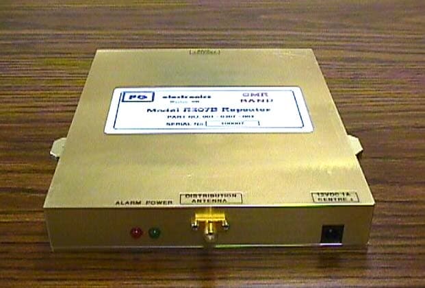
P6T803
Mar 06, 2003Bidirectional SMR Repeater
Equipment Class
AMP - Amplifier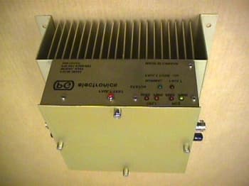
P6T81902
Jun 20, 2002Dual Band Bidirectional Amplifier
Equipment Class
AMP - Amplifier