PD5LMWS11011 Mbps Wireless Access Point
Delta Electronics, Inc.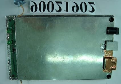
Click to zoom
Application Details
- Equipment Class
- DSS - Part 15 Spread Spectrum Transmitter
- Date of Grant
- Mar 07, 2001
- Application Purpose
- Original Equipment
- Date of Application
- Mar 07, 2001
- Equipment Note
- 11 Mbps Wireless Access Point
- Frequency Range
- 2412.00000000 - 2462.00000000
- Company
- Delta Electronics, Inc.
- Country
- Taiwan
Documents & Files
Document Text
Text extracted from the exhibit documents filed with the FCC. Open a document above to read the original.
Users Manual
Delta Networks Inc. 1 LM-WS110 Wireless Product Specification -- 11Mbps Wireless Access Point Note: This document contains proprietary technical information in which is the property of the Delta Networks Inc. and shall not be disclosed to others in whole or in part, reproduced, copied, or used as the basis for design, manufacturing, or sale of apparatus without written permission of Delta Networks Inc. Delta Networks Inc. 2 Table Of Contents 1. REVISION HISTORY......................................................................................................................................................3 1.1. PRODUCT REVISION HISTORY......................................................................................................................................3 1.2. DOCUMENT REVISION HISTORY...................................................................................................................................3 2. GENERAL DESCRIPTION............................................................................................................................................4 2.1. FEATURES....................................................................................................................................................................4 2.2. MECHANICAL DESIGN..................................................................................................................................................5 2.3. LED DEFINITIONS.......................................................................................................................................................6 2.4. IC SOLUTION...............................................................................................................................................................8 3. TECHNICAL SPECIFICATIONS..................................................................................................................................9 4. DELIVERY PACKAGE.................................................................................................................................................10 4.1. LABELS FOR GIFT BOX AND CARTON.........................................................................................................................10 Delta Networks Inc. 3 1. Revision History 1.1. Product Revision History Revision Date Remark 0 2000/12/22 ß Product Initial 1.2. Document Revision History Revision Date Remark 1.00 2000/12/22 ß Initial specification 1.01 2001/2/6 ß Add Case Photo 1.02 2001/2/12 ß Modify LED definitions ß Change RF activity to RF ready ß Add Ethernet Full/Half LED description ß Delta Networks Inc. 4 2. General Description LM-WS110 is a Wireless-to-Ethernet product. The Wireless interface is IEEE802.11b standard compatible. Its data transmission rate is 11Mbps. The Ethernet interface is IEEE802.3 standard compatible. The data rate is 10Mbps. 2.1. Features ß Complies with the IEEE 802.11b Direct Sequence Specification ß Complies with IEEE 802.3 ß Supports 1, 2, 5.5 and 11 Mbps Data Rate on the wireless interface ß Supports10Mbps Data Rate on the Ethernet interface ß WEP 40-bit data encryption for security ß With Roaming capability ß SNMPv1 management provided ß Remote management via SNMP protocol ß Local management via console port ß Firmware upgrade via console interface ß 5V@800mA power supply needs ß FCC Certified under Part 15 to Operation in 2.4GHz ISM Band ß Delta Networks Inc. 5 2.2. Mechanical Design Delta Networks Inc. 6 2.3. LED Definitions T The LEDs on the LM-WS110 provide visual presentation to show the following status: 3 Status of the system 3 Ethernet Link/Activity 3 Ethernet Full/Half 3 RF Ready Link/Act. Full/Half Power LED Green System is in operation Off Power is off Ethernet Link/Activity LED Solid Green The Ethernet port is at the link status and no data transmission on the port. Blinking Green The Ethernet port is at the link status and there is a data transmission on the port. Off The port is not connected. Note: The link speed is fixed at 10Mbps. Ethernet Full/Half LED Solid Green The Ethernet port is operated at full-duplex mode. But we don’t support full-duplex operation now. Off The Ethernet port is at half-duplex mode. Note: At the current version, this LED is always OFF. RF Ready LED Power RF Ready. Delta Networks Inc. 7 Solid Green Data transmission or receive activity occurs on the port. Off The RF is not ready for data transmission. Delta Networks Inc. 8 2.4. IC Solution The IC solution for LM-WS110 adopts Intersil PRISM II chip set: P/N Functionality Description Atmel AT76C510 Ethernet to Wireless bridge controller. An internetworking device for interconnecting a WLAN with other WLANs and legacy LANs. Wireless interface following the IEEE 802.11 standard. Ethernet MAC Unit interfaces with 10/100 Mbps Ethernet Physical through a standard MII port. Internetworking Unit (INWARM) with integrated ARM7TDMI RISC processor, provides the bridging functions between Ethernet and wireless interfaces. WLAN MAC unit with a second ARM7TDMI and integrated 128-byte Tx and 128-byte Rs FIFOs for wirelss MAC layer functions. Integrated 12Kx32bit internal SRAM for fast program code execution and temporary storage of data. Seeq 80225 Ethernet PHY 10/100Mbps Single PHY Intersil HFA3861B Direct Sequence Spread Spectrum Baseband processor HFA3861B Direct Sequence Spread Spectrum (DSSS) baseband processor is part of the PRISM 2.4GHz WLAN Chip set and contains all the functions necessary for a full or half duplex packet baseband transceiver. The HFA3861B has on-board A/D’s and D/A for analog I and Q inputs and outputs for HFA3783. Intersil HFA3783 I/Q Modulator/Demodulator and Sythesizer HFA3783 is a highly integrated and fully differential SiGe baseband converter for half duplex wireless application. It features all the necessary blocks for quadrature modulation and demodulation of “I” and “Q” baseband signals. Intersil HFA3683A 2.4GHz RF/IF Converter…
Text truncated - open the document above for the full version.
Block Diagram
1 1 11 ANTENNA SWITCH LOW PASS & BAND PASS FILTER TX & RX SWITCH BAND PASS FILTER RF POWER AMPLIFIER HFA3983 RF/IF CONVERTER HFA 3683 VCO 2074MHz RF AMPLIFIER MODULATION DEMODULATION HFA3783 VCO 748MHz BASEBAND PROCESSER HFA3861 3V REGULATOR 2.84V REGULATOR SAW FILTER MAC AT76C510 INPUT POWER REGULATOR SRAM & FLASH ROM Delta Networks Inc., LM-WS110 WIRELESS ACESS POINT Ethernet PHY 80225/B USB Interface BLOCK DIAGRAM 0A3 11Tuesday, February 20, 2001 Title SizeDocument NumberRev Date:Sheetof ANTENNA 1 ANTENNA 2 4 4 3 3 2 2 1 1 55 44 33 22 11 POWER JACK USB PORT ETHERNET PORT ANTENNA {Doc} A3 {Title} A3 11Tuesday, February 27, 2001 Title SizeDocument NumberRev Date:Sheetof
External Photos
Report No.: RF900219021Issued: March 2, 2001 ANNEX 3 PHOTOGRAPHS OF EUT Report No.: RF900219022Issued: March 2, 2001
ID Label/Location Info
FCC ID LABEL LOCATION
Operational Description
FCC ID: PD5LMWS110 ADT No.90021902 Operational Description The transmitter of the EUT (11Mbps Wireless Access Point) is powered by power adapter and connected with notebook through RJ45 port. The antenna is Dual Monople Antenna, there is no antenna connector . Under normal use condition, the user has to keep at least 20cm separation distance between radiator and the body of the user. The other instruction, please have a look at the users manual.
Operational Description
FCC ID: PD5LMWS110 Report No.: RF900219021Issued: March 2, 2001 ANNEX 2 DSSS INFORMATION This device is Direct Sequence Spread Spectrum, the data is mixed by pseudorandom code which is an orthogonal code. The mixed data is digital modulated by BPSK and QPSK technique depends on the data rates. The CCK coding is applied for increasing the data rate, and also the processing gain will be increased. The bit rates are 1,2,5.5,11Mbps, the symbol rates are 1,1,1.375,1.375Mbps, the chip rates are always 11Mbps. So, the Chip/symbol is 11,11,8 and 8 respectively. Although is higher bit rate, the processing gain is lower than 10, but the CCK coding used in higher bit rate will provide 2.2dB coding gain.
Schematics
SCHEMATICS OF LAN HUB FILE NAMEDRAWNDESIGNEDCHECKEDAPPROVED Revision History DescriptionEngineerDate Model No - LM-WS110 Revision Arelease to production02/06 01JEFF.CHIEN LM-WS110.DSN 4AESS-010030 LM-WS110 SERIES ( 5508002393 ) DELTA NETWORK 00 VCCC 00 0 0 0 0 0 00 0 IF_VCO_GND IF_VCO_GND IF_VCO_GND IF_VCO_GND 0 0 0 0 0 0 VCCA 0 0 IF_VCO_GND 0IF_VCO_GND VCCA 0 0 0 0 0 VCCS VCCB VCCC 0 0 0 0 0 +3.3V 0 C21 68pF C18 0.1UF R3 49,9 C16 3,9nF R2 2K C4 220pF C3 100pF R18 100 R17 100 R15 124R12 536 C22 0.1UF R9 536 R6 3,92K R5 2K Q2 IRLML6302 1 32 C15 0,22UF C14 0,022UF C13 0.1UF R22 820 C35 100pF C30 0.1UF C27 100pF C7 1nF C9 1nF C36 22pF C34 220pF C33 220pF C37 22pF C32 220pF R20 1k C19100pF C12 1nF C11 1nF R21 2.87K C31 1nF C26 0.1uF C200.1UF C8 10nF F5F4F3F2F1 68NH 1 2 68NH 1 2 15NH 1 2 F7F6 68nH 1 2 C17 1 180pF U2 F4106-44 4 2 13 VDD GND ENDOUT F10F9F8 R11 124 R16 124 U3 HFA3783 1 2 3 4 5 6 7 8 9 10 11 12 131415161718192021222324 36 35 34 33 32 31 30 29 28 27 26 25 484746454443424140393837 RX_AGC_VCC SPARE IF_RX+ IF_RX- TX_BIAS_GND TX_VAGC TX_BIAS_VCC IF_TX+ IF_TX- TX_AGC_VCC TX_AGC_GND TX_AGC_SUB REF_BYREF_INSYNTH_SUBSYNTH_GNDSYNTH_VDDCLKDATALECP_VDDCP_DOCP_GNDLD RXQ+ RXQ- TXI+ TXI- 1.2V_OUT TXQ+ TXQ- LO_GND LO_VCC LO_IN+ LO_IN- LO_SUB RX_AGC_GND RX_VAGC RX_AGC_SUB IF_DETECT PE1PE2 CAL_EN RX_DEM_GND RX_BB_VCCRX_BB_GND RXI+ RXI- C23 68pF BLM10A121S 12 R23 680 C25 1nF C24 0.1UF RXI- RXQ- RXQ+ RXI+ 1 2 U4 DMP-VCX 2 1 467 5 8 3 GND0 VT GND1GND2GND3 RF GND4 VDD C17 10nF R10 124 C38 0.1uF 1 2 C88 100pF C87 100pF TXQ+ TXQ- TXI- TXI+ C2 10uF C28 0.1UF Q1 MMBT4401 1 3 2 C10 10nF C5 3.3pF C6 3.3pF 27NH 1 2 FL1 SAWTEK855653 9 10 781112 3 4 1256 IN IN_RET GROUNDS3GROUNDS4CASE2CASE3 OUT OUT_RET CASE CASE1 GROUNDS1GROUNDS2 R1 1K C1 10uF C29 1nF U1 MIC5025-2.8 3 1 4 2 5 IN SHDN BP GND OUT SC2 SHORT 1 3 2 I/O_1 NC I/O_2 NO POP DRAWNFILE NAMECHECKEDDESIGNED LAN HUB SCHEMATICS OF APPROVED LM-WS110.DSN 4AESS-010030 LM-WS110 SERIES ( 5508002393 ) DELTA NETWORK 0 0 0 0 VCCC 0 0 0VCCB 0 0 0 0 RF_GND RF_GND RF_GND 0 0 0 0 RF_GND RF_GND RF_GND 0 +3.3V VCCA 0 0 0 00 +3.3V 0 0 0 0 0 +3.3V 0 0 0 0 0 0 00 0 0 0 0 0 RF_GND 0 0 0 0 0 RF_GND 0 0 0 R35 1.5K C71 0.01UF R34 11.5K C70 0.01UF C69 0.01UF R38 0 C77 220pF C76 7pF R37 20 C74 10nF C73 4.7pF C72 0.01UF R36 9.53K C89 0.01UF C84 0.01UF C83 0.01UF C82 0.01UF C81 220pF R40 1.1K C79 0.01UF R39 1.1K U10 DMP-VCX2074S6 2 1 467 5 8 3 GND0 VT GND1GND2GND3 RF GND4 VDD C91 0.01UF C753.3pF C95 0.1UF R461.5K R45649 C92 0.01UF C49 7pF C93 0.68UF 1.2nH 12 R25 180 J1 sma_ra 1 2345 IN GND1GND2GND3GND4 C39 10uF C48 7pF C52 0.01UF 5 2 1 3 4 6 7 IN OUT GND0 GND1 GND2 GND3 GND4 C51 10nF C86100pF C90 0.1uF C85 7pF 4.3nH 12 U11 upg152a 2 3 1 4 5 6 GND OUT2 OUT1 Vcont2 IN Vcont1 C47 7pF J2 sma_ra 1 2345 IN GND1GND2GND3GND4 C46 7pF C45 7pF C98 1nF R41 0 C80 3.3pF C78 3.3pF 68NH 1 2 C50 7pF C140 NOPOP-0.56pF C68 7pF R24 180 C41 7pF R31 10 R30 3.74K R29 3.74K R28 180 C55 7pF R26100 C67 NOPOP-1.5pF C54 7pF 1 2 12 C65 270pF R33 1k C64 7pF R32 10 2.2NH 12 6.8NH 1 2 U8 HFA3983 1 2 3 4 5 6 7 8 9 10 11 12 13 14 29 15 16 17 18 19 20 21 23 24 25 27 28 26 22 GND1 VCC1 PE GND2 VCC2 REXT_OS REXT_DS VCC_DS GND3 GND4 RFOUT GND5 GND6 GND7 PADDLE GND8 GND9 GND10 GND11 GND12 GND13 GND14 GND15 GND16 GND17 GND18 VCC3 DET_OUT RFIN C62 2.7pF R27 180 C63 1pF U12 HFA3683A 1 2 3 4 5 6 7 8 9 10 11 12 13 14 15 16 17181920212223242526272829303132 42 39 44 46 34 35 36 37 48 47 45 43 41 40 38 33 60626455535163615958575654525049 GND1 LNA_VCC1 GND2 RX_IN GND3 BIAS1_VCC1 GND4 H/L PE2 PE1 TX_VCC1 GND5 TXA_OUT GND6 GND7 GND8 TX_VCC1_1GND9TXA_INGND10LEDATACLKREF_BYREF_INGND11SYN_VCC2GND12CP_VCC2CP_DOGND13LD GND15 GND14 GND16 GND17 TX_MX_OUT TX_MX_VCC2 TX_MX_VCC3 TX_MX_VCC4 RX_MX_OUT- TX_MX_IN- RX_LO_DRIVER_VCC1 LO_VCC1 LO_IN- LO_IN+ TX_LO_DRIVER_VCC1 TX_MX_VCC1 GND21GND22GND23GND20GND19GND18 COL_OUT RF_OUT ITAT_RES2 BIAS2_VCC1 PTAT_RES1 ITAT_RES1 PRE_VCC1RX_MX_IN TX_MX_IN+ RX_MX_OUT+ C97 0.1UF C66 0.01UF C61 1nF C59 1nF C58 1nF C57 1nF C56 1nF R42 91 R44 75 R43 75 68NH 1 2 1.8nH 12 1.8nH 12 4 3 2 1 C96 1nF U7 upg152a 2 3 1 4 5 6 GND OUT2 OUT1 Vcont2 IN Vcont1 C60 0.1UF CA1NC CA2 NC C44 0.1UF C43 0.1UF C42 0.1UF C40 10uF C94 0.068UF C99 0.01UF C141 NOPOP-0.56pF 4.7NH 1 2 C53 100pF SC1 SHORT 1 3 2 I/O_1 NC I/O_2 U5 MIC5025-3.0 3 1 4 2 5 IN SHDN BP GND OUT NO POP NO POP In case of AT76C503 rev3, Populate R909 and NOT populate U944 NOTE In case of AT76C503 rev2, Populate U944 and NOT populate R904 See NOTE POPULATE ONLY FOR HFA3861B DRAWNAPPROVEDDESIGNED SCHEMATICS OF CHECKEDFILE NAME LAN HUB LM-WS110.DSN 4AESS-010030 LM-WS110 SERIES ( 5508002393 ) DELTA NETWORK 0 0 00 00 0 0 VCCS 0 0 +3.3V VCCS VCCS U944 nc7sz175p6x 1 34 5 2 6 CLK DQ VCC GND CL C1121000pF R61 10K C105 0.01UF C104 0.1uF C101 10uF C100 10uF R47 0 U15 HFA3861 1 2 3 4 5 6 7 8 9 10 11 12 13 14 15 16 17181920212223242526272829303132 37 43 41 36 40 39 38 35 34 33 42 44 45 46 47 48 64565763626160595855545352515049 GNDD1 VDDD1 SD SCLK R/W CS GNDD2 VDDD2 GNDA1 IIN+ IIN- VDDA2 QIN+ QIN- GNDA2 VREF VDDA3TX_AGC_INRX_IF_DETGNDA3IREFVDDA4IOUT+IOUT-GNDA4COMPCAP2COMPRES2GNDA5QOUT+QOUT-VDDA5COMPRES1 VDDD3 GNDD4 BYP GNDD3 ANT_SEL ANT_SEL RX_RF_AGC TX_IF_AGC RX_IF_AGC COMPCAP1 MCLK TEST0 TEST1 TEST2 TEST3 TEST4 SDI GNDD5VDDD5RESETTX_PERX_PE CCA TX_RDY TXD TXCLK MD_RDY RXD RXCLKTEST7TEST6TEST5 R60 620 R909 0 R490 U945 TC7S04F 1 2 3 5 4 nc in gnd vcc out C110 0.1UF C109 0.1uF C108 0.1UF R57 19.2K R56 19.2K R55 12.1K C107 0.1uF C106 0.1UF C103 0.1uF C102 0.1uF R48 100R C114 0.01UF R59 976R C113 0.1UF R58180R C111 0.01UF DRAWNAPPROVEDDESIGNED SCHEMATICS OF CHECKEDFILE NAME LAN HUBLM-WS110.DSN 4AESS-010030 LM-WS110 SERIES ( 5508002393 ) DELTA NETWORK M_D[7..0 ] M_D[7..0] VCCS VCCS GND_IN VCCS VCCS VCCS VCCS VCCS VCCS VC CS VCCS VCCS VCCS VCCS C91 3 2.2nF j900 USB_B 2 3 4 1 D- D+ GND VCC C923 0.1uF C934 0.1uF C969 NOPOP-0.1uF U904 F4106-32M 4 2 13 VDD GND ENDOUT C900 0.1UF U946 ds1817 1 3 2 RST GND VCC C91410nF C92 1 0.1uF C92 8 0.1uFC922 10nF C925 0.1uF C92 6 0.1uF C927 0.1uF C92 4 0.1…
Text truncated - open the document above for the full version.
Test Report
FCC ID: PD5LMWS110 Report No.: RF90021902 1 Issued: March 2, 2001 FCC TEST REPORT REPORT NO.: RF90021902 MODEL NO.: LM-WS110, LM-WS130 RECEIVED: February 19, 2001 TESTED: February 26, 2001 APPLICANT: Delta Networks, Inc. ADDRESS: No.8, Kon Jan West Road, Liutu Industrial Zone, Keelung, Taiwan, R.O.C. ISSUED BY: Advance Data Technology Corporation LAB LOCATION: 13-1, Lane 19, Wen Shan 3 rd St., Kweishan, Taoyuan Hsien, Taiwan, R.O.C. This test report consists of 48 pages in total. It may be duplicated completely for legal use with the approval of the applicant. It should not be reproduced except in full, without the written approval of our laboratory. The client should not use it to claim product endorsement by NVLAP or any U.S. government agencies. The test results in the report only apply to the tested sample. Accredited Laboratory FCC ID: PD5LMWS110 Report No.: RF90021902 2 Issued: March 2, 2001 Table of Contents 1CERTIFICATION .................................................................................................. 4 2SUMMARY OF TEST RESULTS......................................................................... 5 3GENERAL INFORMATION ................................................................................ 6 3.1GENERAL DESCRIPTION OF EUT ................................................................................ 6 3.2DESCRIPTION OF TEST MODES ................................................................................... 6 3.3GENERAL DESCRIPTION OF APPLIED STANDARDS ............................................... 7 3.4DESCRIPTION OF SUPPORT UNITS.............................................................................. 7 4TEST PROCEDURES AND TEST RESULTS .................................................... 8 4.1CONDUCTED EMISSION MEASUREMENT................................................................. 8 4.1.1LIMITS OF CONDUCTED EMISSION MEASUREMENT ...........................................................8 4.1.2TEST INSTRUMENTS ....................................................................................................................8 4.1.3TEST PROCEDURES ......................................................................................................................9 4.1.4TEST SETUP ..................................................................................................................................10 4.1.5TEST RESULTS .............................................................................................................................11 4.2RADIATED EMISSION MEASUREMENT ................................................................... 17 4.2.1LIMITS OF RADIATED EMISSION MEASUREMENT .............................................................17 4.2.2TEST INSTRUMENTS ..................................................................................................................18 4.2.3TEST PROCEDURES ....................................................................................................................19 4.2.4TEST SETUP ..................................................................................................................................20 4.2.5TEST RESULTS .............................................................................................................................21 4.36dB BANDWIDTH MEASUREMENT ........................................................................... 25 4.3.1LIMITS OF 6 D B BANDWIDTH MEASUREMENT.....................................................................25 4.3.2TEST INSTRUMENTS ..................................................................................................................25 4.3.3TEST PROCEDURE.......................................................................................................................26 4.3.4TEST SETUP ..................................................................................................................................26 4.3.5EUT OPERATING CONDITION...................................................................................................26 4.3.6TEST RESULTS .............................................................................................................................27 4.4MAXIMUM PEAK OUTPUT POWER........................................................................... 31 4.4.1LIMITS OF MAXIMUM PEAK OUTPUT POWER MEASUREMENT......................................31 4.4.2INSTRUMENTS.............................................................................................................................31 4.4.3TEST PROCEDURES ....................................................................................................................32 4.4.4TEST SETUP ..................................................................................................................................32 4.4.5EUT OPERATING CONDITION...................................................................................................32 4.4.6TEST RESULTS .............................................................................................................................33 4.5POWER SPECTRAL DENSITY MEASUREMENT ...................................................... 34 4.5.1LIMITS OF POWER SPECTRAL DENSITY MEASUREMENT ................................................34 4.5.2TEST INSTRUMENTS ..................................................................................................................34 4.5.3TEST PROCEDURE.......................................................................................................................35 FCC ID: PD5LMWS110 Report No.: RF90021902 3 Issued: March 2, 2001 4.5.4TEST SETUP ..................................................................................................................................35 4.5.5EUT OPERATING CONDITION...................................................................................................35…
Text truncated - open the document above for the full version.
Test Report
FCC ID: PD5LMWS110 Report No.: RF90021902 25 Issued: March 2, 2001 4.3 6dB BANDWIDTH MEASUREMENT 4.3.1 LIMITS OF 6dB BANDWIDTH MEASUREMENT The Limit of 6dB Bandwidth Measurement is 0.5 MHz. 4.3.2 TEST INSTRUMENTS Description & ManufacturerModel No.Serial No.Calibrated Until ROHDE & SCHWARZ TEST RECEIVER ESMI 846839/018 848926/005 Mar. 03, 2001 HP ATTENUATOR8496B3247A18505Cal. on use HP PLOTTER7475A2641V27755N/A Notes: 1.The measurement uncertainty is less than +/- 2.6dB, which is calculated as per the NAMAS document NIS81. 2.The calibration interval of the above test instruments is 12 months. And the calibrations are traceable to NML/ROC and NIST/USA. FCC ID: PD5LMWS110 Report No.: RF90021902 26 Issued: March 2, 2001 4.3.3 TEST PROCEDURE The transmitter output was connected to the spectrum analyzer through an attenuator. The bandwidth of the fundamental frequency was measured by spectrum analyzer with 100 kHz RBW and 100 kHz VBW. The 6 dB bandwidth is defined as the total spectrum the power of which is higher than peak power minus 6 dB. 4.3.4 TEST SETUP For the actual test configuration, please refer to the related Item – Photographs of the Test Configuration. 4.3.5 EUT OPERATING CONDITION The software provided by client enabled the EUT to transmit and receive data at lowest, middle and highest channel frequencies individually. EUT SPECTRUM ANALYZER Attenuator FCC ID: PD5LMWS110 Report No.: RF90021902 27 Issued: March 2, 2001 4.3.6 TEST RESULTS EUT11Mbps Wireless Access PointModelLM-WS110 LM-WS130 Environmental Conditions 20°C, 70%RHTe s t e d B ySteven Lu CHANNEL CHANNEL FREQUENCY (MHz) 6 dB BANDWIDTH (MHz) MINIMUM LIMIT (MHz) PASS/FAI L 1 2412 9.470.5PASS 624379.580.5PASS 1124629.580.5PASS FCC ID: PD5LMWS110 Report No.: RF90021902 28 Issued: March 2, 2001 CH1 FCC ID: PD5LMWS110 Report No.: RF90021902 29 Issued: March 2, 2001 CH6 FCC ID: PD5LMWS110 Report No.: RF90021902 30 Issued: March 2, 2001 CH11 FCC ID: PD5LMWS110 Report No.: RF90021902 31 Issued: March 2, 2001 4.4 MAXIMUM PEAK OUTPUT POWER 4.4.1 LIMITS OF MAXIMUM PEAK OUTPUT POWER MEASUREMENT The Limit of Maximum Peak Output Power Measurement is 30dBm. 4.4.2 INSTRUMENTS Description & ManufacturerModel No.Serial No.Calibrated Until HP SPECTRUM ANALYZER8593E3926A04191Mar. 03, 2001 HP ATTENUATOR8496B3247A18505Cal. on use HP PLOTTER7475A2641V27755N/A Notes: 1.The measurement uncertainty is less than +/- 2.6dB, which is calculated as per the NAMAS document NIS81. 2.The calibration interval of the above test instruments is 12 months. And the calibrations are traceable to NML/ROC and NIST/USA. FCC ID: PD5LMWS110 Report No.: RF90021902 32 Issued: March 2, 2001 4.4.3 TEST PROCEDURES 1. The transmitter output was connected to the spectrum analyzer through an attenuator. 2. The center frequency of the spectrum analyzer is set to the fundamental frequency and using 3 MHz RBW and 3 MHz VBW. 3. The span of the spectrum analyzer should be larger than 6dB BandWidth plus 10MHz. 4. Use Peak Search to read the peak power after Maximum Hold function is activated. 5. Shift the marker to +/- 3MHz and +/-6MHz, and record the reading. 6. The Maximum Peak Output Power is the linear summation of the 5 readings in (4) and (5). Note: This measurement is the total power of 15MHz bandwidth which is far more wider than 6dB bandwidth. 4.4.4 TEST SETUP For the actual test configuration, please refer to the related Item – Photographs of the Test Configuration. 4.4.5 EUT OPERATING CONDITION The software provided by client enabled the EUT to transmit and receive data at lowest, middle and highest channel frequencies individually. EUT SPECTRUM ANALYZER Attenuator FCC ID: PD5LMWS110 Report No.: RF90021902 33 Issued: March 2, 2001 4.4.6 TEST RESULTS Output Power Into Antenna: EUT11Mbps Wireless Access PointModelLM-WS110 LM-WS130 Environmental Conditions 20°C, 70%RHTe s t e d B ySteven Lu CHANNEL CHANNEL FREQUENCY (MHz) PEAK POWER OUTPUT (dBm) PEAK POWER LIMIT (dBm) PASS/FAI L 1241217.3630PASS 6243717.7930PASS 11246218.1030PASS FCC ID: PD5LMWS110 Report No.: RF90021902 34 Issued: March 2, 2001 4.5 POWER SPECTRAL DENSITY MEASUREMENT 4.5.1 LIMITS OF POWER SPECTRAL DENSITY MEASUREMENT The Limit of Power Spectral Density Measurement is 8dBm. 4.5.2 TEST INSTRUMENTS Description & ManufacturerModel No.Serial No.Calibrated Until ROHDE & SCHWARZ TEST RECEIVER ESMI 846839/018 848926/005 Mar. 03, 2001 HP ATTENUATOR8496B3247A18505Cal. on use HP PLOTTER7475A2641V27755N/A Notes: 1.The measurement uncertainty is less than +/- 2.6dB, which is calculated as per the NAMAS document NIS81. 2.The calibration interval of the above test instruments is 12 months. And the calibrations are traceable to NML/ROC and NIST/USA. FCC ID: PD5LMWS110 Report No.: RF90021902 35 Issued: March 2, 2001 4.5.3 TEST PROCEDURE The transmitter output was connected to the spectrum analyzer through an attenuator, the bandwidth of the fundamental frequency was measured with the spectrum analyzer using 3 kHz RBW and 30 kHz VBW, set sweep time=span/3kHz. The power spectral density was measured and recorded. The sweep time is allowed to be longer than span/3KHz for a full response of the mixer in the spectrum analyzer. 4.5.4 TEST SETUP For the actual test configuration, please refer to the related Item – Photographs of the Test Configuration. 4.5.5 EUT OPERATING CONDITION The software provided by client enabled the EUT to transmit and receive data at lowest, middle and highest channel frequencies individually. EUT SPECTRUM ANALYZER Attenuator FCC ID: PD5LMWS110 Report No.: RF90021902 36 Issued: March 2, 2001 4.5.6 TEST RESULTS EUT11Mbps Wireless Access PointModelLM-WS110 LM-WS130 Environmental Conditions 20°C, 70%RHTe s t e d B ySteven Lu CHANNEL NUMBER CHANNEL FREQUENCY (MHz ) RF POWER LEVEL IN 3 KHz BW (dBm) MAXIMUM LIMIT (dBm) PASS/FAI L 12412-12.398PASS 62437-12.138PASS 112462-11.988PASS FCC ID: PD5LMWS110 Report No.: RF90021902 37 Issued: March 2, 2001 CH1 FCC ID: PD5LMWS110 Report No.: RF90021902 38 Issued: March…
Text truncated - open the document above for the full version.
Test Report
FCC ID: PD5LMWS110 Report No.: RF90021902 1 Issued: March 2, 2001 ANNEX 1 PROCESSING GAIN OF DIRECT SEQUENCE SPREAD SPECTRUM MEASUREMENT 1. 1.1. 1. LIMITS OF PROCESSING GAIN OF A DIRECT SEQUENCE SPREAD SPECTRUM MEASUREMENT The limit of processing gain is 10dB 1.1 TEST INSTRUMENTS & SUPPORT UNIT Description & ManufacturerModel No.Serial No. Anritsu Spectrum Analyzer, 9kHz to 30GHz MS2667CM10281 Anritsu Signal Generator, 10kHz to 20GHz 68247B984703 Hewlett Packard Power Meter,HP438A2743A04416 Hewlett Packard Power Sensor, -30 to 20dBm 8485A2942A08387 Hewlett Packard Step Attenuator, 10dB steps HP8496B3247A18505 Mini-Circuits Power SplitterZN2PD-9GNA DELL Laptop ComputerInspiron 5000eNA Campaq Laptop ComputerPPX99125 FCC ID: PD5LMWS110 Report No.: RF90021902 2 Issued: March 2, 2001 1.2 METHOD OF MEASUREMENT The processing gain may be measured using the CW jamming margin method. Section 4.7.4 shows the test configuration. The test consists of stepping a signal generator in 50 kHz increments across the passband of the system. At each point, the generator level required to produce the recommended Bit Error Rate (BER) is recorded. This level is jammer level. The output power of the transmitting unit is measured at the same point. The jammer to Signal (J/S) ratio is then calculated. Discard the worst 20% of the J/S data points. The lowest remaining J/S ratio is used when calculating the Process Gain. The reference PER is specified as 8%. The corresponding Es/No (signal to noise ratio per symbol) is 16.4 dB. The curve is attached as below. This value and the measured J/S ratio are used in the following equation to calculate the Process Gain (Gp) of the system. Where: (S/N) o : Signal to noise ratio for the chosen BER. Gp = (S/N) o +Mj+Lsys FCC ID: PD5LMWS110 Report No.: RF90021902 3 Issued: March 2, 2001 Mj : Maximum jammer to Signal Ratio recorded at the detected BER. Lsys : System losses . For the purpose of this processing gain calculation, we assume Lsys at its minimum value of 2 dB. TEST SETUP 7 NOTEBOOK EUT ANRITSU SIGNAL GENERATOR EUT NOTEBOOK PWR SENSOR 8485A Power meter HP 438A Mini-Circuits 15542 ZNZPD-9G HP8496D STEP ATTN 110dB (10dB steps) Matched Cables RECEIVER Transmitter FCC ID: PD5LMWS110 Report No.: RF90021902 4 Issued: March 2, 2001 1.3 TEST PROCEDURES Obtain the simplex link shown. Perform all independent instrumentation calibrations prior to this procedure. Set operating power levels using fixed and variable attenuators in system to meet the following objectives: Signal Power at receiver approximately –55dBm (above thermal sensitivity such that thermal noise does not cause bit errors. Signal Power at power meter between –20 and –30dBm for optimal linearity. Use spectrum analyzer to monitor test. Ensure that CW Jammer generator RF output is disabled and measure the power at the power meter port using the power meter. This is the relative signal power, Sr. Disable Transmitter, and set CW Jammer generator RF output frequency equal to the carrier frequency and enable generator output. Set reference CW Jammer power level at power meter port 8.4dB below Sr (minimum J/S, or 10dB processing gain reference level). Note the power level setting on the generator, this is the reference CW Jammer power setting, Jr. Disable CW Jammer, re-establish link. PER test should be operating essentially error -free. Enable CW Jammer at the reference power level and verify that the PER test indicates a PER of less than 8%. Alternatively, adjust the CW Jammer level to that which causes 8% PER and verify that the S/J is less than 8.4dB. Repeat step 7 for uniform steps in frequency increments of 50 kHz across the receiver passband with the CW Jammer. In this case the receiver passband is +/- 8.5 MHz. The numerical data associated with the following radio channel is tabulated and presented for Channel 1,6, and 11. Note:Since the jamming signal will be blocked by the IF filter if the jamming frequency is far form the center of the carrier frequency. So, only those frequencies ar…
Text truncated - open the document above for the full version.
Contact Information
Applicant
Payton Ting(Manager)
Test Firm
Bureau Veritas CPS (H.K.) Ltd. Taoyuan BranchTommy Wu
Technical Specifications
| # | Rule Parts | Frequency Range | Power Output |
|---|---|---|---|
| 1 | 15C | 2.41 GHz - 2.46 GHz | 64.00 mW |
Other Applications from Delta Electronics, Inc.
PD5-NWA1200
Jun 16, 2026Indoor Wireless AP
Equipment Class
DTS - Digital Transmission SystemPD5-AP743
Jun 03, 2026802.11be enterprise access point
Equipment Class
NII - Unlicensed National Information Infrastructure TXPD5-AP623E
Sep 04, 2025802.11ax enterprise access point
Equipment Class
NII - Unlicensed National Information Infrastructure TX
PD5-LM-WESA04OR
Aug 01, 2021802.11 b/g/n/ac WIFI AP
Equipment Class
NII - Unlicensed National Information Infrastructure TX
PD5-NWA1000
Jul 25, 2021Wireless Access Point
Equipment Class
NII - Unlicensed National Information Infrastructure TX