PGVCB-0800CELLULAR RANGE SMART PHONE
CyberBank Corp
Click to zoom
Application Details
- Equipment Class
- TNE - Licensed Non-Broadcast Transmitter Held to Ear
- Date of Grant
- Apr 26, 2001
- Application Purpose
- Original Equipment
- Date of Application
- Jan 31, 2001
- Equipment Note
- CELLULAR RANGE SMART PHONE
- Frequency Range
- 824.04000000 - 848.97000000
- Company
- CyberBank Corp
- Country
- South Korea
Documents & Files
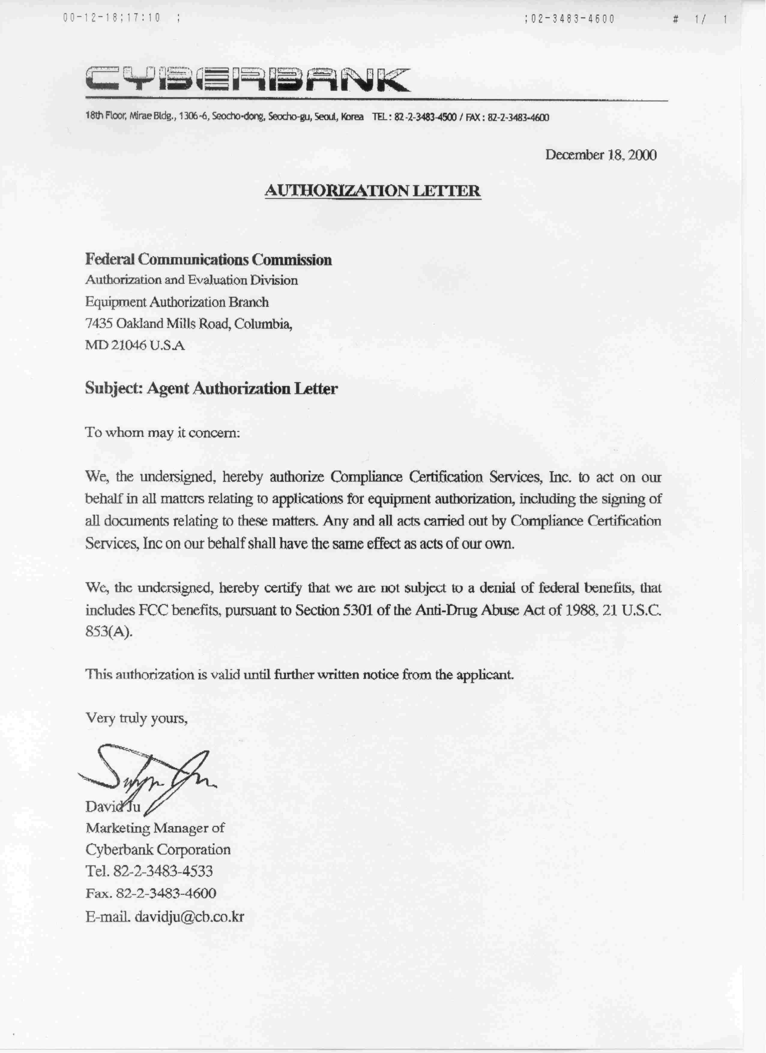
Document Text
Text extracted from the exhibit documents filed with the FCC. Open a document above to read the original.
Users Manual
Chapter 1. Basic Information for Cybird Cybird is a palm-size PC that advanced technologies of mobile computing and wireless communications are combined. Cybird allows data communications as well as data communications to be utilized with a mobile telephone module (CDMA, AMPS, etc.) incorporated in a portable information terminal everywhere and everytime. Supporting resolution of VGA (640 x480), Cyber also allows direct wireless access during moving without changing user’s screen of a conventional Web site or a backbone information system of a company. While conventional portable information terminals require separate cables, mobile telephones or wireless modems, etc. for data communications, Cyber perfectly supports voice communications, wireless data communications and the wireless Internet with only one terminal. In Chapter 1, the following information is described. ! Cybird Fe ature s Components of Cybird are described. ! Reference to Manual Reference to this Manual and details of each Chapter is described. ! Application Programs in Cybird Application programs basically provided in Cybird are introduced. ! Finding Information The web sites to serve Cybird related information including the Windows CE are described. Cybird Features Check first if the following components are included when you purchase Cybird. Please contact immediately the seller if the Cybird you bought has defects or any of the following components is no t incl uded. Body (including a battery pack) Cradle (charger)DC Adapter (220V/60Hz) Lea ther CaseStylus & Co nnectio n StrapUser’s Manual (including a guarantee sheet) Quick ReferenceCustomer Registration CardCybird S/W CD Win CE Service CD (option)Bluetooth Phone (option)Ear Microphone (option) DC Connection Cable (option) Using User’s Manual This Manual was prepared to guide the Cybird users rapidly and easily using the product. Each chapter of this Manual is composed of the following. ! Chap ter 1. Basic Infor ma tion for Cybird Describes components of Cybird and equipped program types, and introduces Internet sites and services to get Cybird-related infor matio n. ! Chapter 2. Starting Cybird Describes key specification of Cybird and general guides to use the Cybird. ! Chapter 3. Setting and Managing Cybird Environment Describes Cybird system setting, management of the battery and memories, etc. and explains utilization of the permanent storage device (IPSM) in the Cybird. ! Chapter 4. Connection to Internet Cybird is allowed to connect to the Internet through direct telephone connection with an incorporated mobile telephone module or using a LAN card of the CF type. This chapter describes how to connect directly to the Internet, and also the Web Browser that is a representative Internet connection program, and the e-mail program. ! Chapter 5. Using Functions of Mobile Telephone Cybird provides voice calls and the Short Message Service (SMS) associated with the functions of a mobile telephone. This chapter describes voice calls, voice call telephone programs and the SMS program to provide the short message service. Principle of Notations Notations in this Manual comply with the following principles to help easy understanding. ! An arrow (•) is used to divide icons and menu items that a user should subsequently select (e.g., Press the menus “Start • Program• Calculator”). ! (Warning) indicates that information is lost or serious faults are caused to Cybird if the user does not comply with the instructions. ! (Caution) indicates damages to the equipment or information loss may be caused if the user does not comply with the instructions. ! (Reference) indicates useful infor matio n in usi ng C ybird. Programs Installed in Cybird Basic programs provided with Cybird include the following. 1. ROM Installation Program The programs installed in the ROM of Cybird can not be deleted or reinstalled arbitrarily. " Phone: The program for voice calls " SMS: The program for sending/receiving short messages " Web Browser: Internet Explorer 4.0 Compatible HTML Browser " MPMail : The program for sending/receiving Internet mails. " Address Book : The program to control the address books. " Sched uler : The user ma na ges the sc hed ule. " Calculator: The program to execute general engineering calculations, measurements conversion, etc. " Recorder: The program to record necessary memos and important matters. " Microsoft Pocket Word: The editor for simple documents. " CF Backup Tool: The program to backup and restore the data stored in the RAM of the Cybird with the CF card and the permanent storage device (may not be provided depending on the model). 2. Programs Provided with CD 1) Game : Socoban, Puzzle and Mole 2) MP3 Player: The program to play MP3 files. 3) Address Book, Scheduler PC Version or Outlook: One of the Address Book and the Microsoft Outlook is provided depending on the model. This program(s) is(are) required for synchronization of the Address Book, the Scheduler program and data installed in Cybird. 4) Microsoft ActiveSync : Is installed in a PC for data synchronization and copy between a PC and Cybird. (Reference) Another programs may be installed other than the application programs basically provided. For more detailed information, see the Chapter 4 “Program Installation/Deletion”. Finding Information (Cybird related information) If you want to find Cybird-related information rapidly, use details in the following table. InformationLocation Windows CE informationhttp://www.microsoft.com/windows/embedded/ce/ Latest Cybird-related information http://www.cb.co.kr/english/products/cybird_1.asp http://www.cb.co.kr/korean/products/cybird_1.asp http://cybird.cb.co.kr Help for ActiveSyncHelp of ActiveSync installed on a PC Help for Cybird“Start → HELP” in Cybird Wireless Internet service sitehttp://www.cybird.net Chapter 2 Starting Cybird In this chapter, basic matters required to use Cybird are described. The information in this chapter includes the following. ! Cybird Fe …
Text truncated - open the document above for the full version.
Block Diagram
3. Block Diagrams & Circuit Schematics3.1 Baseband Logic & Audio Part of Cellular Module PCM CODEC MSM3000 PBGA ARM7 MICROPROCESSOR SUBSYSTEM (CPU) DIGITAL FM PROCESSOR RF INTERFACE CDMA DIGITAL BASEBAND PROCESSOR Serial Bus Interfacefor IFR3000/IFT3000,BBA MAIN UART EVRC VOCODER CODEC_INCODEC_SYNCODEC_CLOCODEC_OU Tx AUDIO FLASH ROM 16Mbit SRAM 2Mbit EEPROM 256KBit SMALL LCD MODULE Rx ADDRESS/DROM_CS/RAM_CS/SERIALSERIAL RegulatorLogic Main & H/W RESET +2.8AV +2.8 V BATTE TX AGC ADRX_AGC_ADTRK_LO_ADPLL_ENABLPLL_DATAPLL_CLKSerial BusInterfaceI_OFFSETQ_OFFSETTX_ IQ_DATARX_ IQ_DATATX_CLK+TX_CLK-ID L E /SLEEP/CHIPX8SYNTH_LOC RF, PLL, IF, IFR3000/IFT3000 Analog Baseband/IF FM/PA ONTCXO/NV BATTE SerialInterface GENERAL PURPOSE INTERFACE (GPIO) Aux PCM or 2nd UART RegulatorAnalogAudio Phone-PDAInterfacePhone-PDAInterface PDA Main, Bluetooth Dual-Port RAM Interface Download & External DM Interface Bluetoo th PCM Interface <Doc> 1.0 CDMA Cellular & PCS ; Logic & Audio Option 1CyBerbank Co., Ltd..Mobile Computer ; CDMA Phone Part 13 Monday, November 20, 2000 TitleSize Document Number Rev Date: Sheet of +2.8V +2.8V_LCD +2.8V +2.8V +2.8V +2.8AV +2.8V VBATT +2.8V I_OFFSETQ_OFFSET IMD_ATTEN(PDM2) TCXO/N TX_IQDATA4 TRK_LO_ADJ TX_IQDATA2TX_IQDATA0 SBST CHIPx8RX_QDATA2 FM_RX_QDATA / RX_IDATA0 RX_IDATA2TX_CLK IDLE/ TX_IQDATA7FM_RX_STB / NOT CONN.(JCDMA)TX_IQDATA5 TX_AGC_ADJ SLEEP/ TX_IQDATA3 SBCK TX_IQDATA1 SBDT RX_QDATA3RX_IDATA3TX_CLK/FM_RX_CLK / NOT CONN.(JCDMA) RX_AGC_ADJ TX_IQDATA6 LOCK RX_QDATA1RX_QDATA0 FM_RX_IDATA / RX_IDATA1 TCXO_IFM / PLL_19.68MHz(JCDMA ) VDDM +2.8AV +2.8V+2.8V_LCD PA_ON PA_R0 FM/ [J_DPX_BW_CTRL]19.68MHz_PLL_EN (J_CDMA)FM/ NOT CONN.(JCDMA) FA14 AD15AD12AD14AD8AD13AD9 FA19 FA13 AD11 FA17FA10FA18 AD10 FA15 AD2AD5 A3 AD[0:7] FA0 AD1 AD6 A[0:9] FA8 AD4 FA3 AD0 A7 FA4 AD3 A1 AD5 FA5 A4A8 AD1 AD6 A9 AD7 AD7 FA6FA2 AD0 FA9FA1FA7 A2 AD3 AD4 A5A6 AD2 FA11FA12FA16 ROM_CS2/ LWR/ RD/ R830 0 C817open C815open R854 0 C823100pFC822open R861100 R801 1K C81210nF C805 1nF C866open C8131nF C811100nF R853 0 ohm[open for MSM3000] R852 0 ohm[open for MSM3000] R851 0 ohm[open for MSM3000] R818 0 U804 RD28F1604C3B90 A1A2 A4 A3 A5A6A7A8 A9 A10A11A12 G6B4B5B6B7 B8 B9B10E10E9E8E6E5 E4E3D8 D7 D5D4D3 C10C9C8C7 C5C4C3F3F4F5 F7F8F10F9 H1H2H3 H4H5H6 H7H8H9 H10H11H12G10 G9G8G7B3G5G4G3 D9 D10 DUDU A11 A20 A15A14A13A12 F-GNDF-VccqDUDU A6A8 A10 A9 DQ15 S-WE/ DQ14 DQ7DQ3DQ2 DQ10DQ11 A19 F-VppF-WP/S-CS2 DQ12 A22F-RP/S-GND DQ5DQ4DQ6 DQ13 A21DUF-WE/S-LB/S-UB/S-OE/ DQ9DQ8DQ1DQ0 DUDUDU A5A4A0 F-CE/F-GNDF-OE/DUDUDUS-CS1/ A1A2A3 A16 A7 A17A18 S-VccF-Vcc R808 330 C855 10nF C86010nF C804 1nF R805 1K R804 1K C803 1nF C853 1uF(#) C854 100nF R83747K Reserved0 ohm U808ILC7082AIM5-28 12 4 3 5 VinGND Byp ON Vout R843 OPEN R8500 ohm[open for MSM3000] R828open / DEL(JCDMA) C875OPEN [1uF] C85610nF C857100nF R82410K U802 MSM5000PBGA-196 [MSM3000] L4 K4 D1N3 K3 M1 N9K5 M2 L3 N1 N2 M9 P11 L10 B12M10P12N12M11P13N13 M12 L11L12 M14N14 M13 G11G13H14H13H12H11 J14J13J12J11 K14K13K12K11 L14L13 D11C12B13B14D12C13E10C14E12D13E11D14F12E13E14F11G12F14F13G14B11C11A12A13 B10C10D10A11B5C7A7A8C8D4 C3 B2 E4E3E1E2D3D2H1H4C2B1C1H2L2J2J1H3J4K1K2J3L1G4G3G2G1F4F3F2F1 P2 P3 M4N4A2C4B3E5A3 A10 M3 P9M8L9P10N10C5B4D5A4C6A5D6A6B6D7B7B8A9B9C9D9P5L6M6N6P6L7M7N7P7N8L8P8 P4 L5 M5N5 F10 J10 E9K9E6K6F5 J5 G10 H10 F9 G9 H9 J9 E8 F8 G8 H8 J8 K8 E7 F7 G7 H7 J7 K7 F6 G6 H6 J6 G5 H5 P1 A14 P14 A1 D8 N11K10 PA_ONSYNTH_LOCKSLEEP/TRK_LO_ADJTX_AGC_ADJRX_AGC_ADJ GPI029GPI030 IDLE/ PA_R0 PA_R1 LNA_RANGE RESIN/RESOUTWDOG_ENWDOG_STB_PCMSCSXTAL_INXTAL_OUTLWR/RD/LCD_ENHWR/ PA_ON2 RAM_CS2/RAM_CS1/ROM_CS1/ROM_CS2/ LNA_GAIN D15D14D13D12D11D10D9D8D7D6D5D4D3D2D1D0A19A18A17A16A15A14A13A12A11A10A9A8A7A6A5A4A3A2A1A0PCM_CLKPCM_SYNCPCM_DINPCM_DOUT AUX_PCM_CLK AUX_PCM_SYNC AUX_PCM_DIN AUX_PCM_DOUT TMSTCK TDO TDI TRST/ TMODE MODE1MODE0 FM_RX_IDATA FM_RX_QDATA FM_RX_STB FM_RX_CLK I_OFFSET Q_OFFSET TX_CLK TX_CLK/ ADC_ENABLE_SBST ADC_DATA_SBDT ADC_CLK_SBCK CHIPX8 TCXO TX_IQDATA7TX_IQDATA6TX_IQDATA5TX_IQDATA4TX_IQDATA3TX_IQDATA2TX_IQDATA1TX_IQDATA0 C_RX_IDATA3 C-RX_IDATA2 C_RX_IDATA1C_RX_IDATA0 C_RX_QDATA3C_RX_QDATA2C_RX_QDATA1C_RX_QDATA0 PDM1 PDM2 YAMN1 RINGER KEYSENSE0/KEYSENSE1/KEYSENSE2/KEYSENSE3/KEYSENSE4/ LCD_CS/GP_CS/ GPIO_INT0GPIO_INT1GPIO_INT2GPIO_INT3GPIO_INT4 GPI00GPI01GPI02GPI03GPI04GPI05GPI06GPI07GPI08GPI09 GPI010GPI011GPI013GPI014GPI015GPI016GPI017GPI018GPI019GPI020GPI021GPI022GPI023GPI024GPI025GPI026GPI027GPI028 DP_TX_DATADP_RX_DATACTS/RFR/VDDVDDVDDVDDVDDVDDVDDVDD GND GND GND GND GND GND GND GND GND GND GND GND GND GND GND GND GND GND GND GND GND GND GND GND NC NC NC NC GPIO12 SLEEP_XTAL_INSLEEP_XTAL_OUT R8471k R84410K R816300 C81422pF R83447K C830 10nF C829 100nF C831100nF C873 open U801 X84256S8I-2.5 2 4 1 3 8 7 5 6 I/O Vss CE/ WP/ Vcc NC WE/ OE/ C83710nF R827 470 C84447pF C845 47pF R829 100 C871100nF C8722.2uF(#) C87010nF R810 1K C836 100nF C835 10nF C8021nF C8101nFC8091nF R802 0 U806 open[TC7SH08FU] 2 4 5 3 1 In A Out Vcc Gnd In B U805 open[TC7SH08FU] 2 4 5 3 1 In A Out Vcc Gnd In B C852 100nF C851 33uF(@) C839 47pF R8111K R803 1K R849 0 ohm[open for MSM3000] C8582.2uF(%) R809 open C842 1nF C84047pF R826 470 C841 10nF C843 10uF(%) X801 32.768KHz 4.7K 10K 47K 47K Q812 UMC5N 312 45 R846 1M C828 10nF R823 100 C838 100nF R8391M C82110uF(%) D801 DAN222 12 3 C827 100nFR819open C825 10uF(%) L801 CIB21P470 R820 0 C849 open C848 open X802 SSR_27MHz C847 open R8120 R817 0 C816open C834 100nF U807 STw5093 16201921 14 221727 15 26 123456789 10111213 18232425282930 GndP CCLK BZ CS- VLr+ CI VFr Dx VLr- Gnd VccRemOutReminMic3+Mic3-MBiasVccAMic1+Mic1-GndAMic2+Mic2-VccP LO AuxClk VccIO CO Dr FS MCLK R807100K C876 100nF(JCDMA) C865 2.2uF(#) U803 open[TC7SH08FU] 2 45 31 In A OutVcc GndIn B C833 10uF(%) C864470pF R83810K C86910nF J8…
Text truncated - open the document above for the full version.
Block Diagram
1.Introduction 1.1 Summary of CDMA Digital Cellular Communication Mode The CDMA(Code Division Multiple Access) method adopts the direct sequence mode from the spread spectrum communication modes which have been used mainly for military communication equipment. By greatly improving securability and increasing subscriber capacity, it can afford to accept several times as large as the capacity for existing analog communication mode, to overcome difficulty in call connection in a densely populated area such as the Metropolitan area, and to ease inconvenience of call disconnection by means of soft/softer handoff, hard handoff, and dynamic RF power control technology. The CDMA digital cellular communication network is composed of MSO(Mobile Switching Office), BSC(Base Station Controller), BTS(Base Station Transmission System), and MS(Mobile Station), and the communication protocol between MS and BTS is designed to have compatibility with American IS- 95A(Common Air Interface) and domestic TTA-related radio access standard. The related standards of MS are as follows: ! IS-95A/B(Common Air Interface) : Mobile Station - Base Station Compatibility Standard for Dual-Mode Wideband Spread Spectrum Cellular System : Protocol standard between MS and BTS ! IS-98A/B(Recommended Minimum Performance Standards for Mobile Stations) : Minimum performance standards relating to hardwares of MS 1.2 Frequency Allocation and Use !Transmit frequency band : 824 MHz ~ 849 MHz ! Receive frequency band : 869 MHz ~ 894 MHz !Channel spacing : 1.23 MHz ! Transmit/Receive frequency spacing : 45 MHz ! The number of channels : 20 ! Receive frequency of MSO FA No. Channel No. Center Frequency (MHz) FA No. Channel No. Center Frequency (MHz) 11011824.64011404837.120 229825.87012445838.350 370827.10013486839.580 4111828.33014527840.810 5152829.56015568842.040 6193830.79016609843.270 7234832.02017650844.500 8275833.25018697845.910 9316834.48019738847.140 10363835.89020779848.370 ! Transmit frequency of MSO FA No. Channel No. Center Frequency (MHz) FA No. Channel No. Center Frequency (MHz) 11011869.64011404882.120 229870.87012445883.350 370872.10013486884.580 4111873.33014527885.810 5152874.56015568887.040 6193875.79016609888.270 7234877.02017650889.500 8275878.25018697890.910 9316879.48019738892.140 10363880.89020779893.370 2. Electrical Specifications 2.1 General Transmit Frequency824 MHz ~ 849 MHz Receive Frequency869 MHz ~ 894 MHz Radio TypeG7W Number of Frequency Channels(FA) 20 Channel Spacing1.23 MHz Power Supply 2.9V~4.2Vdc, Regulated 2.8Vdc internally used Idc(max)<700mAH[depends on field strength] Sleep State Current Drain1.2mA(typ.)<2mA(max.) Wake_Up Rx Standby Current85mA(typ.)<100mA(max.) Average Standby CurrentDepends on Slot Mode Operating Temperature-20• • +50• Storage Temperature-40• • +125• Dimension 33 x 66 x 5 mm³ Weight19.0 g 2.2 Transmitter Maximum Output Power 316 mW(25dBm) ±50% Waveform Quality> 0.944 Occupied Bandwidth< 1.32 MHz Open loop power control range @ -25 dBm=Rx (Open Loop Power Control Range) -48 ±9.5 dBm(-57.5 dBm<-38.5 dBm) Open loop power control range @ -65 dBm=Rx -8 ±9.5 dBm(-17.5 dBm<1.5 dBm) Open loop power control range @ -104 dBm=Rx 18dBm<30dBm Closed Loop Power Control Range< ±24 dB Minimum Output Power< -50 dBm < -42dBc @ > 900KHz, RBW=30KHz or @ > 1.385MHz, RBW=1MHz or both < -60dBm / RBW=30KHz < -55dBm / RBW=1MHz Co nd ucted Sp urio us Emissi o ns < -54dBc @ > 1.98MHz, BW=30KHz or @ > 2.465MHz, RBW=1MHz or both < -60dBm / RBW=30KHz < -55dBm / RBW=1MHz Frequency Accuracy < ±300 Hz 2.3 Receiver < FER 0.5% @-104 dBm Receiver Sensitivity and Dynamic Range < FER 0.5% @ -25 dBm Single-Tone Desensitization< FER 1.0% @-101dBm Interfering Tone –30 dBm @ 900 KHz offset < FER 1.0% @-101dBm -43dBm @ 900KHz, 1700KHz offset < FER 1.0% @ -90dBm -32dBm @ 900KHz, 1700KHz offset Intermod ul atio n Sp urio us Response Attenuation < FER 1.0% @ -79dBm -21dBm @ 900KHz, 1700KHz offset < -81dBm / 1MHz@ 869~894MHz < -61dBm / 1MHz@ 824~849MHz Co nd ucted Sp urio us Emissi o ns < -47dBm / 30KHz@ for all other frequenc ies 3. Block Diagrams & Circuit Schematics3.1 Baseband Logic & Audio Part of Cellular Module PCM CODEC MSM3000 PBGA ARM7 MICROPROCESSOR SUBSYSTEM (CPU) DIGITAL FM PROCESSOR RF INTERFACE CDMA DIGITAL BASEBAND PROCESSOR Serial Bus Interfacefor IFR3000/IFT3000,BBA MAIN UART EVRC VOCODER CODEC_INCODEC_SYNCODEC_CLOCODEC_OU Tx AUDIO FLASH ROM 16Mbit SRAM 2Mbit EEPROM 256KBit SMALL LCD MODULE Rx ADDRESS/DROM_CS/RAM_CS/SERIALSERIAL RegulatorLogic Main & H/W RESET +2.8AV +2.8 V BATTE TX AGC ADRX_AGC_ADTRK_LO_ADPLL_ENABLPLL_DATAPLL_CLKSerial BusInterfaceI_OFFSETQ_OFFSETTX_ IQ_DATARX_ IQ_DATATX_CLK+TX_CLK-ID L E /SLEEP/CHIPX8SYNTH_LOC RF, PLL, IF, IFR3000/IFT3000 Analog Baseband/IF FM/PA ONTCXO/NV BATTE SerialInterface GENERAL PURPOSE INTERFACE (GPIO) Aux PCM or 2nd UART RegulatorAnalogAudio Phone-PDAInterfacePhone-PDAInterface PDA Main, Bluetooth Dual-Port RAM Interface Download & External DM Interface Bluetoo th PCM Interface <Doc> 1.0 CDMA Cellular & PCS ; Logic & Audio Option 1CyBerbank Co., Ltd..Mobile Computer ; CDMA Phone Part 13 Monday, November 20, 2000 TitleSize Document Number Rev Date: Sheet of +2.8V +2.8V_LCD +2.8V +2.8V +2.8V +2.8AV +2.8V VBATT +2.8V I_OFFSETQ_OFFSET IMD_ATTEN(PDM2) TCXO/N TX_IQDATA4…
Text truncated - open the document above for the full version.
Block Diagram
3. Block Diagrams & Circuit Schematics 3.1 Baseband Logic & Audio Part of Cellular Module PCM CODEC MSM3000 PBGA ARM7 MICROPROCESSOR SUBSYSTEM (CPU) DIGITAL FM PROCESSOR RF INTERFACE CDMA DIGITAL BASEBAND PROCESSOR Serial Bus Interface for IFR3000/IFT3000, BBA MAIN UART EVRC VOCODER CODEC_IN CODEC_SYN C CODEC_CLO CK CODEC_OU T Tx AUDIO FLASH ROM 16Mbit SRAM 2Mbit EEPROM 256KBit SMALL LCD MODULE Rx ADDRESS/D ATA ROM_CS/ RAM_CS/ SERIAL CLOCK SERIAL DATA Regulator Logic Main & H/W RESET +2.8AV +2.8 V V_BATTE TX_AGC_AD RX_AGC_AD J TRK_LO_AD J PLL_ENABL E PLL_DATA PLL_CLK Serial Bus Interface I_OFFSET Q_OFFSET TX_IQ_DATA RX_IQ_DATA TX_CLK+ TX_CLK- IDLE/ SLEEP/ CHIPX8 SYNTH_LOC K RF, PLL, IF, I FR3000/IFT3000 Analog Baseband/IF FM/ PA_ON TCXO/N V_BATTE Serial Interface GENERAL PURPOSE INTERFACE (GPIO) Aux PCM or 2nd UART Regulator Analog Audio Phone-PDA Interface Phone-PDA Interface PDA Main, Bluetooth Dual-Port RAM Interface Download & External DM Interface Bluetooth PCM Interface 3.2 Radio Frequency Part of Cellular Module ANT1 800MHz Cellular Mobile Station CDMA/AMPS Dual_Mode RF BlockDiagram IFT3000 (U514) MSM3000 PBGA (U802) TXIF TXIF/ RF/IF PLL (U508) TCXO VCTCXO 19.68MHz (U509) TX_AGC_ADJ RX_AGC_ADJ DUPLEXER (F501) DOWN MIXER (U517) RF BPF (F503) AMPS RX IF BPF (F502) L.O. BUFFERAMPLIFIER (Q506, Q508) TX IF BPF (F507) UP MIXER (U516) TXIF AMP (Q510) RF BPF (F506) POWER AMP (U515) Revised date : 2000.01.11 Revised by : NaBogyu LNA (Q504) CDMA RX IF BPF (F504) sw TRK_LO_ADJ DUAL PLL VCO PLL CONTROL RXIF VCO TANK RXVCO_T1 RXVCO_T2 RXVCO_OUT RX V_CONT RFVCO_OUT RFV_CONT RF VCO (U507) VCO TANK TX V_CONT TX FREQ. : 824-849MHz RX FREQ. : 869-894MHz IMD_CONTROL I.L. of ANT to RX : -3.5dB I.L. of TX to ANT : -3.5dB G=16dB NF=1.5dB I.L.=-2.5dB G=15dB I.L.=-5dB I.L.=-10dB G=-55 ~ +45dB I.L.=-5dB ADC_IN1 (HPDT) G=0dB I.L.=-2.5dBG=28dB I.L.=-0.5dB 953.5~978.5MHz G=10dB 85.38MHz SBI[3] (85.38MHz) (260.76MHz) (170.76MHz) RX Pmin = D:-108dBm A:-116dBm TX Pmax = D:+25dBm A:+28dBm D:-111.5dBm A:-119.5dBm D: -98.0dBm A:-106.0dBm D: -95.5dBm A:-103.5dBm D:-95.0dBm D:-83.0dBm D:-58.0dBm +37dB A:-103.0dBmA:-98.0dBm +45dB D:+28.5dBm A:+31.5dBm D:+29.0dBm A:+32.0dBm D: 1.0dBm A:+4.0dBm D:+3.5dBm A:+6.5dBm D:+3.5dBm A:+6.5dBm D:-11.5dBm A:-8.5dBm D:-6.5dBm A:-3.5dBm D:-16dBm A:-23dBm -6dBm +3dBm -3dBm D:CDMA A:AMPS -13dBm -7dBm -10dBm A:-58.0dBm RX_AGC_ADJ IFR3000 (U503) TXIF PLL I Q D I V 2 RX VCO G=-70~+20dB DAC[8] TX VCO DIV2 I Q (0 ~25dB) TX_AGC_ADJ TX / Control Registor ADC_IN1/2/3 ADC_IN2 (BATTERY) ADC_IN3 (TEMP) ADC_IN1 (HPDT) TXD[8] TX_CLK[2] G=15dB ADC RX/Control Registor SBI[3] RXD[8] RX_CLK[2] I_OFFSET Q_OFFSET TCXO/N CHIPx8
Cover Letter(s)
Federal Communication Commissions 7435 Oakland Mills Road Columbia MD 21046 Attention: Mr. Steven Dayhoff Subject: Applicant:CyberBank, FCC ID:PGVCB-0800 Confirmation No:EA99938 Application Date:02/01/2001 Dear Steve:Date:3/21/2001 Along with this cover letter, I am uploading the necessary files to support the request to change the status from Deferred to Technical Review. The original device was tested as PDA with AMP cellular phone, which was filed to the Commission on 02/01/2001. Right after the submission, Cyberbank has come out the new device, which is PDA with AMP/CMDA dual mode Cellular phone. In accordance to Mr. Frank Coperich’s E-mail dated on 3/05/2001: “ This application has been assigned to Mr. Steven Dayhoff for review. As a pending application, it is eligible for modification prior to Grant. However, only one version of this device may be approved under one FCC ID. To avoid unnecessary review of the currently pending application, you should submit a request for deferral - until the revised material is sent. When re- activated, the application will be reviewed in order of it's original receipt date. Please contact Mrt. Dayhoff to coordinate this process.” The proposed FCC ID number: PGVCB-0800 will be assigned to PDA with AMP/CDMA dual mode Cellular phone only. There will be no FCC ID number to associate with PDA with AMP Cellular phone. If Cyberbank decides to sell PDA with AMP Cellular phone, new FCC application with new FCC ID number will be made to the Commissions. Due to urgency of this application, Cyberbank has requested Mr. Scott Johnson from law firm of Gardner, Carton & Douglas to assist the review process. However, if there is any technical question you may have, please direct your questions to Compliance Certification Services. Best Regards Mike Kuo / Vice President Compliance Certification Services Tel : (408)463-0885 x:105 Fax: (408)463-0888 E-mail:[email protected]
ID Label/Location Info
PROPOSED FCC ID LABEL AND LOCATION CYBERBANK CORPORATION This device complies with part 22 of FCC rules. FCC ID: PGVCB-0800 FCC ID LABEL LOCATION
Operational Description
4. Theory of Operation 4.1 Logic Section 4.1.1 DC Distribution and Regulation Part Energizing the battery and pressing "END" key on the phone screen of the display shorts "VBATT" and "ON_SW", and U811 and U808 "+2.8V" regulator are enabled through D801, resulting in supplying power for U802 MSM main system processor and other digital circuits. At the same time, the reset output of U811, is applied to Q812 which are (Power On) reset circuits and "RESET/" and "RESIN/" signals are created to reset U802 processor, U804 memory. On the other hand, the battery voltage inputted as "ON_SW" turns ON Q801 to output "Low" to "ON_SW_SENSE/" port of MSM3000. MSM3000 receives this signal and recognizes that "END" (Power) key is pressed and maintains the power through D801 by outputting "High" through PS_HOLD signal. U811 +2.8V power is used for MSM3000, U804 Memory, digital section on U503 IFR3000, U514 IFT3000, U807 PCM Audio Codec and other digital circuits. U808 +2.8 AV power is supplied for Audio, the analog section on U807 STw5093, and other analog circuits. U502 supplies +2.8V power for RF Rx; U505 for VC-TXCO(System Timing Reference Clock), PLL, and VCO; U520 for RF Tx IF & Mixer. Power for RF Tx Power Amplifier is supplied directly from the battery. 4.1.2 Logic Part 4.1.2.1 Summary The logic part is composed of MSM3000 ARM-7 processor core-combined CDMA ASIC, flash ROM & SRAM, and EEPROM. The MSM3000 is CDMA ASIC chipset which is implemented for system control and baseband digital signal processing on the terminal equipment. In order for MSM3000 to operate, CHIPx8, which is a signal transmitted from TCXO Clock and IFR3000, and external resonator are necessary. These generate the CPU clock built in MSM3000. Major components used for the logic section are as follows: 1) MSM3000: U802, [ARM-7 processor core + CDMA signal processing + EVRC] ASIC 2) Flash ROM & SRAM: U804, 16 Mbit flash memory & 2 Mbit static RAM 3) EEPROM: U801, 256 kbit serial-interface EEPROM 4.1.2.2 Baseband Digital Signal Processing MSM3000(Mobile Station Modem) is a core device for CDMA mode, containing ARM-7 CPU core. MSM3000 is composed of a single chip and of 196 pin PBGA package type, and the features and specifications of the clock are recapped as follows: 1) It interfaces IFR3000 & IFT3000 on RF section directly in CDMA mode. 2) It contains internal Vocoder which has even EVRC feature. 3) It is designed to interface RF section which makes power control circuit. 4) It has a built-in ARM-7 MicroProcessor Core. 5) It has a built-in watch dog timer. 6) It has a 64 byte FIFO(First Input First Output) serial data port. 7) It provides 31 GPIO(General Purpose Input Output) ports. 8) It provides 10 Interrupt Ports. (Of these, 5 ports are used to interface the key pad.) 9) It supports external DTMF ringer circuit. 10) It supports 8/16 bits external SRAM and EEPROM. 11) It has chip select feature for the exter nal ROM, RAM, and EEPROM. 12) It provides A0-A19 address buses and AD0-Ad15 data buses. The configuration by feature of the inside of MSM3000 is as follows: 1. Microprocessor Core MSM3000 has a built-in ARM-7 MicroProcessor Core, and this MicroProcessor contains Interrupt Controller, Timer/Counter, and DMA Controller. In addition, 16 bit datapath is included, and addressing up to 1 Mbyte can be performed and I/O space can be extended up to 1Mbyte. Although it is necessary to provide Clock from the outside in order to operate MicroProcessor, this system provides Clock by using 27 MHz resonator. 2. Input Clock 1) CPU Clock(27 M Hz): This becomes the Clock needed for MicroProcessor built in MSM3000 to operate. 2) TCXO(19.68 MHz) Clock: This is the reference clock for controlling EVRC Vocoder and SLEEP mode, and it is also the whole system reference clock. 3) CHIPx8(9.8304 MHz): This is a Clock derived from 19.68 MHz TCXO Clock which is supported from IFR3000 of RF section and becomes the Timing Reference Clock for CDMA signal processing. 3. CDMA Core This is the part for processing CDMA signals in CDMA mode, and it is composed of Demodulator, Modulator, and Decoder. 1) Demodulator: This is composed of 4 demodulating fingers, 1 searcher engine, deinterleaver, time tracking part, and symbol combiner, and it implements such functions as forward link CDMA signal processing and timing acquisition. 2) Modulator: This implements such functions as the encoding and interleaving of CDMA signal on reverse link, controlling the operation of IFT3000 on RF section in CDMA mode, and performing the automatic monitoring the status of IFT3000. 3) Decoder: This implements Viterbi decoding on CDMA forward link. CDMA Core and IFR3000/IFT3000 Interface 1) Transmitter: 8bit TX I and Q data are inputted in D/A converter inside IFT3000, and I data and Q data are stored in I DAC on rising edge of TX clock and Q DAC on falling edge of of TX clock, respectively. TX_CLK+ and TX_CLK- become the reference clock for 8 bit D/A converter inside IFT3000 at TX. 2) Receiver: Components such as analog I and Q baseband inside IFR3000 are converted to digital signals by the two and same 4 bit flash A/D converter. CDMA A/D converter is outputted as a new digital value at falling edge of CHIPx8(9.8304 MHz) which is the reference clock and inputted into MSM3000. 4. RF Interface This interfaces RF section to control power amplifier, TxLO buffer amplifier, VC-TCXO, and AGC-end on the transmit/receive paths. 1) Transmitter Interface: This sends TX_ADJ signal to TxAGC amplifier to adjust transmit power level; it sends PA_O N signal to control power amplifier. 2) Receiver Interface: This sends RX_AGC_ADJ signal to Rx AGC Amplifier to adjust receive path gain; it sends TRK_LO_ADJ signal to RF section to control TCXO frequency automatically(AFC). …
Text truncated - open the document above for the full version.
Parts List/Tune Up Info
Cybird Specification Rev 0.1 11/17/2000 Contents 1. Overview 2. Basic Description 2.1 B lock Dia gram 2.2 Clock Block Diagram 3. Design Specification 3.1 Processor 3.2 Memory System 3.3 Perip h eral Controller 3.4 LCD Module 3.5 CCFL Back light 3.6 Inverter 3.7 Input System 3.8 External Port 3.9 Speaker & Microphone 3.10 Battery 3.11 Cradle 3.12 Adapte r 3.13 Software 1. Overview The Cybird product is the Cyberbank’s definition of a smart-phone running the Microsoft WinCE 3.0 Operation System. Cybird shall be a pocketable product very capable in maintaining the users personal information as well as providing mobile phone with wireless communication. 2. Basic Description The Cybird product contains the following features: - Mobile Phone (CDAM Module (800Mhz)) - Intel SA1110 based design - Full VGA(640X480) TFT LCD - CCFL Backlight - Touch panel - One Compact FLASH Type II slot - Microphone for voice input - Speaker for audible output - Li-Ion Rechargerable Battery - Charger & Cradle 2.1 Block Diagram Figure is a block diagram view of the Cybird PDA part showing the major functional components and their relationships. 1) System Block Diagram 2.2 Clock Block Diagram CDMA Interface LCD(VGA) & Touch Panel Power Module & Voltage Detector Compac t Flash Socke…
Text truncated - open the document above for the full version.
Contact Information
Applicant
Russel Kim(R & D Manager)
Technical Contact
COMPLIANCE CERTIFICATION SERVICESTOM COKENIAS
[email protected]408-463-0885
561 F MONTEREY ROAD · MORGAN HILL, California · United States
Non-Technical Contact
COMPLIANCE CERTIFICATION SERVICESCLAUDIA J PEREZ
[email protected]408-463-8118
Test Firm
Compliance Certification Services IncSteve Cheng
Technical Specifications
| # | Rule Parts | Frequency Range | Power Output | Emission | Tolerance |
|---|---|---|---|---|---|
| 3 | 22H | 824.04 MHz - 848.97 MHz | 354.00 mW | 40K0F1D | 2.5 ppm |
Other Applications from CyberBank Corp

PGVCP-X515
Feb 19, 2006PDA
Equipment Class
TNE - Licensed Non-Broadcast Transmitter Held to Ear
PGVCB-0880NP
Apr 10, 2005Triton / Pocket PC CDMA Phone
Equipment Class
JBP - Part 15 Class B Computing Device Peripheral
PGVCP-X315
Mar 23, 2005CDMA Pocket PC/POZ PDA Cellular Phone
Equipment Class
TNE - Licensed Non-Broadcast Transmitter Held to Ear
PGVCB-2460
Nov 10, 2002PDA
Equipment Class
JBP - Part 15 Class B Computing Device Peripheral
PGVCB-9020-US
Jan 20, 2002Personal Digital Assistant
Equipment Class
JBP - Part 15 Class B Computing Device Peripheral