PISWAP-1100E2.4GHz Wireless LAN
Widelink Co., Ltd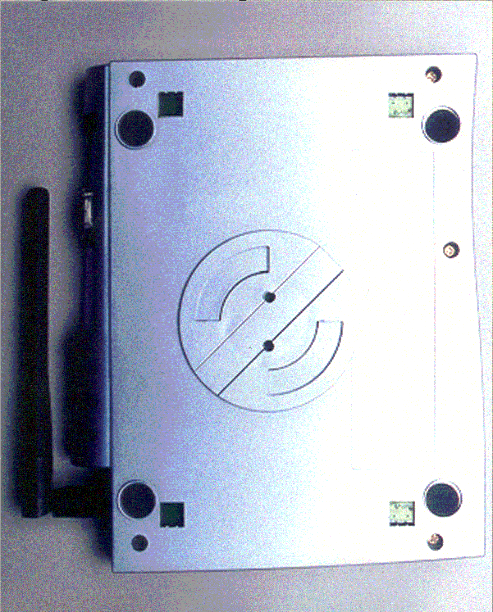
Click to zoom
Application Details
- Equipment Class
- DSS - Part 15 Spread Spectrum Transmitter
- Date of Grant
- Jul 05, 2001
- Application Purpose
- Original Equipment
- Date of Application
- Jul 05, 2001
- Equipment Note
- 2.4GHz Wireless LAN
- Frequency Range
- 2400.00000000 - 2483.50000000
- Company
- Widelink Co., Ltd
- Country
- South Korea
Documents & Files
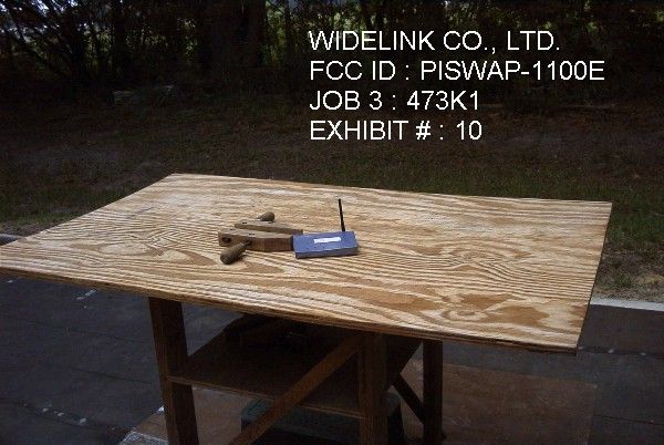
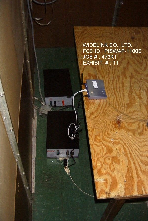
Document Text
Text extracted from the exhibit documents filed with the FCC. Open a document above to read the original.
Users Manual
ezWAVE Access Point Users’ GuideVersion 1.6 Copyright© Widelink 2000DOC – 2001.02.01 Page 1 of 50 WAP-1100 Series Wireless LAN Access Point Users’ Guide Corporate Headquarters Widelink Co. Ltd. 664-25 Dongshin Bldg. 2F Shinsa-Dong, Kangnam-gu Seoul 135-120, Korea http://www.widelink.co.kr Tel:+82-2-3445-9938 Fax:+82-2-3445-8534 ezWAVE Access Point Users’ GuideVersion 1.6 Copyright© Widelink 2000DOC – 2001.02.01 Page 2 of 50 Contents Chapter 1Introduction To The Wireless LAN........................ 5 1.1 What is Wireless LAN?.............................................5 1.2 Wireless LAN Standard and Structure.................................6 Chapter 2Setup ezWAVE Access Point............................12 2.1 Before You Begin Installation .................................... .... 12 2.2 Installing The Widelink ezWAVE WAP-1100 Series Access Point ............................................14 Adjust the antennas ................................................ 14 Ethernet Cable Connection ....................................... 15 Connect The Power Pack ......................................... 16 Connect Serial Cable ............................................... 17 Open Terminal Program ........................................... 18 Configuration Change .............................................. 21 2.3 Verifying the Operation of the ezWAVE Access Point .......... 28 Chapter 3Access Point Management...................................30 3.1 Starting Configuration Tool...............................................31 Access Point Connection...........................................32 Access Point Configuration Window.............................33 Terminal Window for Diagnosis ..................................37 Firmware Upgrade Window .......................................38 Firmware Upgrade Via Internet ..................................39 Firmware Upgrade Via Local Disk................................41 Access Point Detail Control........................................42 3.2 Setting Bridge Mode ..................................................... 43 Chapter 4Troubleshooting..................................................45 ezWAVE Access Point Users’ GuideVersion 1.6 Copyright© Widelink 2000DOC – 2001.02.01 Page 3 of 50 Appendix Appendix ACell Planning (Radio Range) ............................................46 Appendix BTechnical Specification ...................................................48 Appendix CChannel Allocation ........................................................ .50 ezWAVE Access Point Users’ GuideVersion 1.6 Copyright© Widelink 2000DOC – 2001.02.01 Page 4 of 50 THE SPECIFICATIONS AND INFORMATION REGARDING THE PRODUCTS IN THIS MANUAL ARE SUBJECT TO CHANGE W ITHOUT NOTICE. ALL STATEMENTS, INFORMATION, AND RECOMMENDATIONS IN THIS MANUAL ARE BELIEVED TO BE ACCURATE BUT ARE PRESENTED WITHOUT WARRANTY OF ANY KIND, EXPRESS OR IMPLIED. USERS MUST TAKE FULL RESPONSIBILITY FOR THEIR APPLICATION OF ANY PRODUCTS. THE SOFTWARE LICENSE AND LIMITED WARRANTY FOR THE ACCOMPANYING PRODUCT ARE SET FORTH IN THE INFORMATION PACKET THAT SHIPPED W ITH THE PRODUCT AND ARE INCORPORATED HEREIN BY THIS REFERENCE. IF YOU ARE UNABLE TO LOCATE THE SOFTWARE LICENSE OR LIMITED WARRANTY, CONTACT YOUR WIDELINK REPRESENTATIVE FOR A COPY. NOTWITHSTANDING ANY OTHER WARRANTY HEREIN, ALL DOCUMENT FILES AND SOFTWARE OF THESE SUPPLIERS ARE PROVIDED “AS IS” WITH ALL FAULTS. WIDELINK AND THE SUPPLIERS DISCLAIM ALL WARRANTIES, EXPRESSED OR IMPLIED, INCLUDING WITHOUT LIMITATION, THOSE OF MERCHANTABILITY, FITNESS FOR A PARTICULAR PURPOSE AND NONINFRINGEMENT OR ARISING FROM A COURSE OF DEALING, USAGE, OR TRADE PRACTICE. IN NO EVENT SHALL WIDELINK OR ITS SUPPLIERS BE LIABLE FOR ANY INDIRECT, SPECIAL, CONSEQUENTIAL, OR INCIDENTAL DAMAGES, INCLUDING WITHOUT LIMITATION, LOST PROFITS OR LOSS DAMAGE TO DATA ARISING OUT OF THE USE OR INABILITY TO USE THIS MANUAL, EVEN IF W IDELINK OR ITS SUPPLIERS HAVE BEEN ADVISED OF THE POSSIBILITY OF SUCH DAMAGES. SAFETY INFORMATION WARNING * Opening the unit, for whatever reason, could lead to damages that are not covered by the guarantee. * To prevent fire or shock hazard, do not expose your ezWAVE wireless LAN PC cards to rain or moisture. NOTES: * The Widelink supplied software may show screens slightly different from those included in this manual. * This manual is written based on the assumption that you are familiar with basic operations of Windows operating system. Microsoft Windows, Windows95, Windows98, Windows ME, Windows 2000 and Windows NT are registered trademarks of Microsoft Corporation. ezWave, Widellink’s logo, is registered trademark of Widelink Co., Ltd. or its affiliates in Korea, US and certain other countries. All other trademarks mentioned in this documents are the property of their respective owners. The use of word partner does not imply a partnership relationship between Widelink and any of its resellers . Using the Widelink’s ezWAVE card Copyright ⓒ2000. Widelink Co., Ltd. All rights reserved. ezWAVE Access Point Users’ GuideVersion 1.6 Copyright© Widelink 2000DOC – 2001.02.01 Page 5 of 50 Chapter 1 Introduction To The Wireless LAN A wireless LAN (WLAN) is a flexible data communication system implemented as an extension to, or as an alternative for, a wired LAN within a building or campus. Using electromagnetic waves, WLANs transmit and receive data over the air, minimizing the need for wired connections. Thus, WLANs combine data connectivity with user mobility, and, through simplified configuration, enable movable LANs. WLANs have gained strong popularity in a number of vertical markets, including the health-care, retail, manufacturing, warehousing, and academic arenas. These industries have profited from the productivity gains of using hand-held terminals and notebook computers to transmit real-time information to centralized hosts for processing. Today WLANs are becoming more widely recognized as a general-purpose connectivity alternative f…
Text truncated - open the document above for the full version.
Block Diagram
Copyright© 2000 Widelink Co., Ltd. 01-04-30 1 of 2 1. Blockdiagram of RF Board Digital B ’ d Interface Copyright© 2000 Widelink Co., Ltd. 01-04-30 2 of 2 2. Blockdiagram of Digital Board MPC860 RJ45 DB-9 RF Module Interface 32bit 8bit 11bit 21bit LXT905 DS1834A Fail LED SDRAM 4/16/32Mbyte Flash ROM 512K /1/2Mbyte MAX3221 Link LED Software Reset HRESET Port D[7]Port D[9] GPL0/1/2/3 CS1 PCMCIA Data Bus Interface Bus Address Bus CS0 SCC1 SMC1 Regulator LT1086 3.3V 5~12V/1.5A SDRAM Control
ID Label/Location Info
Copyright© 2000 Widelink Co., Ltd. 01-07-03 1 of 1 FCC MARKING/LABEL FOR PART 15 FCC ID : PISWAP-1100E MODEL NO.: WAP-1100E THIS DEVICE COMPLIES WITH PART 15 OF THE FCC RULES. OPERATION IS SUBJECT TO THE FOLLOWING TWO CONDITIONS : (1) THIS DEVICE MAY NOT CAUSE HARMFUL INTERFERENCE, AND (2) THIS DEVICE MUST ACCEPT ANY INTERFERENCE RECEIVED, INCLUDING INTERFERENCE THAT MAY CAUSE UNDESIRED OPERATION.
Operational Description
Copyright© 2000 Widelilnk 01-04-30 3 of 28 1. Introduction This paper describes the ezWAVE AP circuits, specifications,layouts and partlist etc. 2. Circuit Description 2.1 The Architecture The radio design is centered on the expected signal characteristics of the modulation method. A Differential Quadrature Phase Shift Keying (DQPSK) modulation encodes the data in terms of phase with minimal amplitude variation, improving noise immunity. This is joined with the IEEE 802.11 protocol standard Carrier Sense Multiple Access/Collision Avoidance (CSMA/CA) and with the FCC requirement for 10dB processing gain, to allow signals to be received with approximately 0dB Signal to Noise Ratio (SNR) for a 10 -5 Bit Error Rate (BER). The CSMA/CA protocol allows only one user, per channel, at a time (i.e., first come, first serve) making for a quieter medium. The processing gain, achieved by spreading the signal with a PN code, allows a faint signal to be pulled from the noise while suppressing non-correlating interferers. From the antenna, the received input is applied to the pre-select filter FL1. This filter is a two pole dielectric design, rejecting interferers outside the 2.4GHz ISM band and providing image rejection. The signal enters the HFA3683 RF/IF Converter, first passing through the integrated LNA section and then enters the down converter section of the HFA3683. Low-side local oscillator injection is used to mix down to the single intermediate frequency, 374MHz. The IF receive filter FL3, is a Surface Acoustic Wave (SAW) device used for channel selection within the band. The SAW output is reactively matched to the IF input of the HFA3783 Quadrature IF Modulator/Demodulator. In receive mode, the HFA3783 provides two limiting amplifiers, a quadrature baseband demodulator, and two baseband low pass filters. The two limiting amplifiers or limiters provide most of the receiver gain, giving the radio itís sensitivity. The baseband circuit samples the waveform with 7-bit ADCs and then despreads and demodulates the received data. On the Transmit side, data can either be DBPSK or DQPSK modulated at 1MSPS (Mega Symbols Per Second), resulting in a baseband quadrature signal with I and Q components . These digital signals are output to the HFA3783 fifth order Butterworth low pass filters, which are used to provide shaping of the phase shift keyed (PSK) signal. The required transmit spectral mask, at the antenna, is -30dBc at the first side-lobe relative to the main lobe. The signals are then quadrature modulated up to IF using the same 2xLO used for the quadrature Copyright© 2000 Widelilnk 01-04-30 4 of 28 demodulation. The signal then goes to the high impedance input of the HFA3683 upconverting mixer for conversion to the 2.4GHz - 2.5GHz band. The mixer output goes to the pre-amplifier, in the HFA3683, amplifies the signal and easing the requirement for HFA3983 RFPA gain. FL2, a two pole dielectric bandpass filter, is used to suppress both transmit LO leakage and the undesired sideband. The HFA3983 RFPA amplifies the transmit signal to approximately +18dBm. The transmit sidelobe performance is approximately -30dBc. Allowing for a 3dB loss in the band select filter FL1, this gives a final output power of +15dBm. 2.2 Transmit Chain Front End Cascade Analysis The large gain in the Power Amplifier, HFA3983, keeps the signal level small for the whole chain before it. This helps conserve supply current and the cost associated with devices that need to handle large signals. The output power at the RF filter is shown as 15dBm, with the output of the Power Amplifier at 18dBm. The design has been optimized for the best use of supply current and cost of the PA. If the output power was lower, the supply current and cost of the PA could be saved with smaller and cheaper devices. If the output power was higher, the signal will be too close to the P1dB and the signal will have excessive distortion, causing regrowth of the side lobes. The transmitted signal must suppress side lobes to -30dB to meet the 802.11 spectral mask specification. Therefore, the output power needs to be controlled very carefully. The run to run variation in gain and insertion loss of the elements in the transmit chain requires either a manual power adjustment or an active power adjustment feedback circuit. In this design, a manual potentiometer is used to adjust output power and side lobe performance on each unit during manufacturing. For purposes of this analysis, the variable attenuator shows 0dB loss and the Modulator output as -12dBm. This was done for illustration purposes only, in actuality the Modulator output has a relatively large output (200mV P-P ) that needs to be significantly attenuated to the level indicated. 2.3 Power Amplifier(HFA3983) The HFA3983 is fabricated in the fastest SiGe BiCMOS process available, allowing superior RF performance, normally found only in GaAs ICs. Cost effective functions, normally requiring external components, are integrated into one IC. The HFA3983 integrates the following functions in one compact 28 pin EPTSSOP: Two Stage, 30dB Gain RFPA, Logarithmic power detect function (15dB Dynamic Range), CMOS level compatible Power Up/Down function, Single Supply, 2.7V to 3.6V Operation. The HFA3983 contains a highly linear RFPA designed to deliver 18dBm and meet an ACPR specification of -30dBc in the 2.4 to 2.5GHz ISM band. The performance of this two stage RFPA can be optimized by adjusting the bias current in each stage with a dedicated resistor. No external Copyright© 2000 Widelilnk 01-04-30 5 of 28 positive or negative power supplies are required to set the bias currents. The on chip bias network provides the optimum bias current temperature compensation when low TC external resistors are used. To get the best performance from the HFA3983, the output stage matching network can be tailored using external components. 2.4 2.4GHz RF/IF Converter and Synthesizer(HFA3683) The HFA3683A is a monolithic SiGe half …
Text truncated - open the document above for the full version.
Schematics
CHECK-2DATE 1/4 WAP-1100E_SUB 4 CUSTOMER 5 Widelink (PCMCIA_1) 1231234567 6 AB BCD E DESIGNCHECK-1 CD E A 76 11 0 S-XY 22KR1 REMARK UPDATE SHEET REV. 4 1 0.1uFC8 DGND S-XY 6 VCC5 11 S-XY 109 S-XYS-XY 1 2 5 3 S-XY S-XYS-XY 13 01 12 C9 10uF 12 C200.1uF 3 4 0.1uFC21 11 DGND 560R14 DGND 83 VCC_IO3 VCC_IO4 98 VCC_IO5 105 VSS_CORE1 13 24 VSS_CORE2 VSS_CORE3 37 115 VSS_IO1 VSS_IO2 52 67 VSS_IO3 VSS_IO4 82 97 VSS_IO5 VSS_IO6 42 XTALI 40 XTALO 41 S-XY PL5 1211 PL6 93 PL7 RESET 16 20 RXC RXD 19 10 TCLKIN TRST 62 18 TXC TXD 17 VCC_CORE1 14 25 VCC_CORE2 39 VCC_CORE3 53 VCC_CORE4 VCC_IO1 124 VCC_IO2 66 8 PJ5PJ6 7 9 PJ7 35 PK0PK1 3433 PK2PK3 6364 PK4PK5 2122 PK6PK7 2315 PL0PL1 2726 PL2PL3 2843 PL4 MD13 4645 MD14MD15 44 59 MD2MD3 5857 MD4MD5 5655 MD6MD7 54 51 MD8MD9 50 PJ0 3130 PJ1PJ2 3229 PJ3PJ4 65 90 MA16MA17 9192 MA18MA2 7475 MA3MA4 7677 MA5MA6 7879 MA7MA8 8081 MA9 61 MD0MD1 60 49 MD10MD11 4847 MD12 99 HD2 HD3 6 5 HD4 HD5 4 3 HD6 HD7 2 96 HD8 HD9 95 MA0 7273 MA1MA10 84 MA11 8586 MA12MA13 8788 MA14MA15 89 108 HA2 HA3 109 110 HA4 HA5 111 112 HA6 HA7 113 117 HA8 HA9 118 HD0 101 100 HD1 94 HD10 HD11 128 127 HD12 HD13 126 125 HD14 HD15 123 *HINPACK 103 120 *HIORD *HIOWR 119 *HIREQ 114 121 *HOE *HREG 102 36 *HSISCHG 104 *HWAIT *HWE 116 70 *MOE*MWEL 7168 *NVCS*RAMCS 69 38 CLKOUT 106 HA0 HA1 107 2 S-XYS-XY 01 6 U3 HFA3841 1 *HCE1 *HCE2 122 10 11 DGND 0 1011 DGND VCC5 0 C190.1uF S-XY T9 S-XY 9 R26 VCC5 VCC5 C30.1uF S-XY 8 8 1 R9 47K 47KR1147K 3 4 7 8 VCC5 S-XY 0 1 S-XY 5.62KR42 5612 S-XYS-XY VCC5 04 21 12 L3 BLM21P300S 47K47KR17 5 6 0 2 S-XY 54 22KR78 R21 89 S-XY S-XY R622K 0.1uFC2 2 S-XYS-XY 23 R10 47K 4 1 121415 S-XY 0 C10210uF 1 162 S-XY 47KR8 R747K 13 3 A8 2 A9 I_O0 2122 I_O1 23 I_O2I_O3 2526 I_O4I_O5 27 I_O6 2829 I_O7 NC 9 VCC 824 VSS 15 6 *WE 5 20 A0A1 19 A10 31 A11 1 12 A12A13 4 11 A14 7 A15A16 10 18 A2 17 A3A4 1615 A5A6 14 A7 6 3 VCC5 VCC5 7 16 U1 IS62LV1024LL 32 *OE 30 *OE1*OE2 3.3V 14 0.1uFC1 C6 0.1uF 0.1uF C14 2 3 S-XYS-XY 0.1uFC7 23 +3.3V 0.1uFC81 S-XY 3.3V S-XY C310.1uF 1 10 34 DGND 6 R1222K 18 S-XY S-XY DGND DGND 3 76 7 S-XY 109 7 L17 01 8 1716 1 1514 S-XYS-XY 1312 1314 BLM21P300S 1 4 R72 1K S-XY DGND DGND 6 S-XYS-XY R185.62K 22KR16 DGND 1311 S-XY 14131716 R422K C100.1uF 0.1uF C5 17 98 7 3 7 22KR2 S-XY 9 S-XYS-XY 10uFC34 12 S-XYS-XY 9 NC 8 VCCVSS 24 4 5 1 R7922K S-XY A2 18 A3 1716 A4A5 1514 A6 13 A7A8 3 A9 221 I_O0I_O1 22 I_O2 2325 I_O3I_O4 2627 I_O5 28 I_O6I_O7 29 IS62LV1024LL U4 *OE 32 *OE1 30 6 *OE2 5 *WEA0 2019 A1 31 A10 1 A11A12 12 4 A13A14 11 A15 7 10 A16 A6 14 A7 13 3 A8 2 A9 DQ0 2122 DQ1 23 DQ2DQ3 2526 DQ4DQ5 27 DQ6 2829 DQ7 NC1 96 NC2 VCC 824 VSS *OE1 3032 *OE2*WE 7 20 A0A1 19 A10 31 A11 1 12 A12A13 45 A14 11 A15A16 10 18 A2 17 A3A4 1615 A5 AGND 15 13 11 C40.1uF U2 AM29LV0108 7 8 S-XY 54 32 S-XY AGND 47KR5 VCC5 8 5 54 15 12 3 S-XY 15 R86 33K S-XY 10 9 DGND S-XY DGND 1514 14 GEN_MODE 0 DGND VCC5 5 12 13 9 10 GEN_MODE MA(19:0) MFM_CIRL(4:0) TX_PECCAMD_RDYPA_PEPE(2)SD_RF_IFLE_RFSCLK_RF_IF MD(15:0) MA(19:0) HCE(2)* HOE* HWE* HIORD* HIOWR* HWAIT* HIREQ* HREG* HINPACK* HSTSCHG* HRESET MD(15:0) RX_PERESET_BB*T_R_SW*CAL_EN 44MHZ_REF MD(7:0) MFM_CIRL(4:0) HD(15:0) HA(9:0) HCE(1)* S_CLKS_DATACSBPE(1)LE_IFWLAN_LINK RADIO_PD MA(19) T_R_SWRX_CLKRX_DATATX_CLKTX_DATA 6 CD E ABCD E DESIGNCHECK-1CHECK-2 SHEET REV. CUSTOMER DATE 0 S-XYS-XY REMARK UPDATE 4 2/4 WAP-1100E_SUB (PCMCIA_2) 2 5 Widelink 3 7 6 11234 AB 5 54 S-XY 0R19 1 S-XY C25 1000PF DGND 98 AGND DGND 976R30 1 C139 0.01uF DGND S-XYS-XY R23 0 0R27 2 VDDD1 8 VDDD2 37 VDDD3 VDDD4 57 16 VREF S-XY S-XY S-XY S-XY S-XYS-XY C140 0.01uF TEST2 4647 TEST3TEST4 48 TEST5 49 50 TEST6 TEST7 51 TXCLK 55 58 TXD TX_AGC_IN 18 35 TX_IF_AGC 62 TX_PE TX_RDY 59 12 VDDA1 17 VDDA2 VDDA3 22 31 VDDA4 QIN+ 1314 QIN- 29 QOUT+ QOUT- 30 52 RXCLK RXD 53 RX_IF_AGC 34 19 RX_IF_DET RX_PE 61 RX_RF_AGC 38 5 R_*WSCLK 4 SD 3 64 SDI TEST0 4445 TEST1 GNDA2 15 GNDA3 20 25 GNDA4 GNDA5 28 GNDD1 1 GNDD2 7 GNDD3 3643 GNDD4 56 GNDD5 10 IIN+IIN- 11 23 IOUT+ IOUT- 24 21 IREF MCLK 42 54 MD_RDY 14 HFA3861U5 39 *ANT_SEL *CS 6 *RESET 63 ANT_SEL 4041 BYP 60 CCA 33 COMPCAP1 COMPCAP2 26 COMPRES1 32 27 COMPRES2 GNDA1 9 0.1uF C26 R32 12.1K AGND AGND S-XY 12 0.1uFC13 S-XY S-XY AGNDAGND 7 S-XYS-XY S-XY AGND 560R20 C1510uF S-XY AGND 0.1uFC30 7 0 0 S-XY R3419.1K 910 S-XYS-XY 2 S-XY 2 DGND R28619 AGND 13 4 S-XY S-XY R1310K S-XYS-XYS-XY S-XY R29 0 0.1uF C29 S-XYS-XY VCC5 AGND AGND 10uFC11 12 C120.1uF S-XYS-XY 6 0.1uF C18 0.1uFC35 44 RFSH 58 RFU SPKR* 6364 STSCHG* VCC1 17 52 VCC2 18 VPP1 VPP2 5360 WAIT* WE*_PGM* 15 S-XY S-XY C17 0.1uF D8 6566 D9 GND1 134 GND2 36 GND3GND4 69 INPACK* 61 IOIS16* 33 IORD* 4546 IOWR* 16 IREQ*LED1 35 70 LED2 OE* 9 62 REG* RESET 59 CE1* 7 CE2* 43 30 D0D1 31 D10 6738 D11D12 3940 D13D14 4142 D15 32 D2 2 D3D4 34 D5D6 56 D7A2 27 50 A20A21 5154 A22A23 5556 A24A25 57 26 A3A4 2524 A5A6 2322 A7 12 A8A9 11 CD1* 3768 CD2* S-XY CON1 CON_70 A0 2928 A1 8 A10 10 A11A12 21 A13 1314 A14 20 A15A16 19 A17 4748 A18A19 49 S-XY R22 100 S-XYS-XY 5 S-XY 76 43 C36 0.1uF C32 0.1uF 56 1112 1 S-XY 15 8 S-XY 3.3V DGND DGNDDGND S-XY S-XY 32 HCE(1)* HOE* HWE* HIREQ* HD(0:15) HA(0:9) WLAN_LINK +3.3V 3 S-XY 19.1KR33 S-XY RXQ+ RXQ- 44MHZ_REF TEST(0:7) TX_CLK HCE(2)*HIORD*HIOWR*HRESETHWAIT*HINPACK*HREG*GEN_MODEHSTSCHG* RX_DATA RX_IF_AGCIF_DET RX_PE RX_RF_AGC S_DATA S_CLK TX_DATA TX_DET TX_IF_AGC TX_PE VREF RXI+ RXI- ANTSEL* RESET_BB* ANTSEL CCA CSB TXI+TXI- MD_RDY TXQ+TXQ- RX_CLK A CD E E BCD DATEDESIGNCHECK-1CHECK-2 REV. REMARK UPDATE SHEET 5 CUSTOMER 3/4 Widelink (PCMCIA_3) WAP-1100E_SUB 4 12 2345 B 3 1 67 6 A 3.92KR55 C107 3900PF S-XY 49.9R56 0.1uFC135 0.022uFC91 0R64 AGND 100PFC108 AGND C13610uF 12 IN_RET 12 OASE 1 OASE1 3 OUT OUT_RET 4 R57 0 220PFC39 15PFC46 FL1 SAW374M 5 6 8 7 GROUND 11 GROUND1 2 IN 910 0.1uFC84 220PFC56 L6 22NH S-XY C121 C12068PF C51 10PF 39NH L5 0.1uFC133 0.1uF MAX8867 1 *SHDNBP 5 GND 2 IN 34 OUT AGND 0.1uF C72 C1370.1uF U13 ENFVZ5F81 4 GND1 GND2 5 6 GND3 GND4 7 8 GND5 RF 1 VCC 23 VCONT U15 SYNTH_GND 16 15 SYNTH_SUB 17 SYNTH_VDD TXI+ 3433 TXI- 31 TXQ+ TXQ- 30 TX_AGC_GND 1112 TX_AGC_SUB 10 …
Text truncated - open the document above for the full version.
Schematics
R3 DATEREMARK UPDATE SHEET REV. CUSTOMER 1/5 WAP-1100E_MAIN 4 1 5 Widelink (MPC860) 3 1 2 5 3.3V 3.3V S-XY S-XY 4 D E 67 6 AB 23 C ABCD E DESIGNCHECK-1CHECK-2 R71 2.7K S-XY S-XY GND S-XY 100nFC33 2.7kR70 25 S-XY L4 8.2mH 10 S-XY S-XY S-XYS-XYS-XY 2.7kR98 S-XYS-XY 1KR107 S-XY S-XY 22 R170 50 22 S-XY S-XY S-XY R91 2.7K S-XY S-XY 2.7kR133 R125 2.7k 3.3V GND 9 1631 S-XY S-XY R165 2.7k R155 2.7k R72 1K S-XY S-XY 1KR111 S-XYS-XY 31 S-XY S-XY S-XY 27 S-XY 29 S-XY S-XYS-XY 1KR93 R83 1K 1913 S-XY S-XY 3.3V 2.7kR134 R167 2.7k S-XY R116 2.7K 12 100nFC46 10uF_16VC30 12 TP7 S-XY S-XY S-XY 13 2.7kR100 S-XY S-XY S-XY 10nFC32 1112 S-XY S-XY S-XY S-XY 11 S-XY S-XY S-XY R66 2.7k S-XY S-XY GND GND S-XY GND S-XY GND S-XYS-XY 3 R79 1K R23 2.7K 50R171 S-XY 7 GND S-XY S-XY R84 2.7K S-XY GND 23 2 S-XY 6 2.7kR109 S-XY S-XY S-XY S-XY S-XY 18 S-XY S-XY R87 2.7K 2.7KR852.7kR158 S-XY 4 S-XYS-XY S-XY R112 1K S-XY GND S-XY 19 3.3V R69 50 R22 2.7K S-XYS-XYS-XY 30 S-XY S-XY S-XY S-XY S-XY S-XY 24 S-XY S-XY S-XY GND S-XY R99 2.7k 14 S-XYS-XY 28 S-XY 3.3V 2.7KR97 R108 2.7K 1 S-XY S-XY 29 89 S-XY S-XY S-XY S-XY 3.3V S-XY S-XY S-XY 3.3V S-XY S-XY J3 CON10C 1 10 2345 67 9 R129 2.7k R101 2.7K S-XY 3.3V R156 50 50R164 S-XY 310 P16T14 VDDH5 VDDL1 A8M1 VDDL2VDDL3 H19W8 VDDL4 VDDSYN T1 VSSSYN U1 V1 VSSSYN1 C7 WE0 WE1 A6 B6 WE2 WE3 A5 T2 XFC P1 XTAL S-XY R9R10 VCC35VCC36 R11R12 VCC37VCC38 R13R14 VCC39 E8 VCC4 VCC40 R15 VCC5 E9E10 VCC6VCC7 E11E12 VCC8VCC9 E13 F4 VDDH1VDDH2 F16P4 VDDH3VDDH4 VCC2 VCC20 K5K15 VCC21 L5 VCC22VCC23 L15 VCC24 M5M15 VCC25 N5 VCC26VCC27 N15P5 VCC28VCC29 P15 VCC3 E7 VCC30 R5R6 VCC31 R7 VCC32VCC33 R8 VCC34 N3 TMS G18 G19 TRST TSIZ0_*REG B9 C9 TSIZ1 VCC1 E5 VCC10 E14E15 VCC11 F5 VCC12VCC13 F15 VCC14 G5G15 VCC15 H5 VCC16VCC17 H15 VCC18 J5J15 VCC19 E6 U17 PD3 W16 U16 PD4 PD5 U15 V16 PD6 PD7 T15 W17 PD8 PD9 V17 B2 RD_*WR SPARE1 B7 H18 SPARE2 SPARE3 V15 H4 SPARE4 H16 TCK TDI H17 TDO G17 TEXP J19F18 PC12PC13 E18D18 PC14PC15 D16T17 PC4PC5 T18R19 PC6PC7 M16M18 PC8PC9 L18 W18 PD10 PD11 T16 R16 PD12 PD13 V18 V19 PD14 PD15 PB17 PB18 N17 N19 PB19 PB20 L16 K16 PB21 PB22 L19 K17 PB23 PB24 J18 J16 PB25 PB26 F19 E19 PB27 PB28 D19 E16 PB29 PB30 C19 C17 PB31 K19 PC10PC11 G16 F17 PA12 PA13 E17 D17 PA14 PA15 C18 R18 PA2 PA3 P17 P19 PA4 PA5 N18 M17 PA6 PA7 M19 L17 PA8 PA9 K18 PB14 U18 R17 PB15 PB16 N16 P18 IP_B0 IP_B1 J3 J2 IP_B2 IP_B3 G1 G2 IP_B4 IP_B5 J4 K3 IP_B6 IP_B7 H1 R1 KAPWR L4 OP0 L2 OP1 OP2 L1 M4 OP3 U19 PA0 PA1 T19 J17 PA10 PA11 GND9 D7 GPL_A0 GPL_A1 C6 B5 GPL_A2 GPL_A3 C5 C1 GPL_A4 GPL_A5 D3 GPL_B4 B1 T5 IP_A0IP_A1 T4 U3 IP_A2IP_A3 W2 U4 IP_A4IP_A5 U5 T6 IP_A6IP_A7 T3 H2 GND68GND69 N11 F12 GND7 N12 GND70GND71 N13N14 GND72 GND73 P6P7 GND74GND75 P8P9 GND76GND77 P10P11 GND78GND79 P12 GND8 F13 P13 GND80GND81 P14F14 L13L14 GND54GND55 M6M7 GND56GND57 M8M9 GND58GND59 M10 GND6 F11 M11 GND60GND61 M12M13 GND62GND63 M14N6 GND64GND65 N7N8 GND66GND67 N9N10K8 GND4 F9 K9 GND40GND41 K10K11 GND42GND43 K12K13 GND44GND45 K14L6 GND46GND47 L7L8 GND48GND49 L9 F10 GND5 L10 GND50GND51 L11L12 GND52GND53 H11H12 GND25GND26 H13H14 GND27GND28 J6J7 GND29 F8 GND3 GND30 J8J9 GND31GND32 J10J11 GND33GND34 J12J13 GND35GND36 J14 GND37 K6K7 GND38GND39 GND1 GND10 G6G7 GND11GND12 G8G9 GND13GND14 G10G11 GND15GND16 G12G13 GND17GND18 G14H6 GND19 GND2 F7 GND20 H7H8 GND21GND22 H9H10 GND23GND24 D25D26 U7V12 D27D28 V6W5 D29 W10 D3 D30 U6T7 D31 D4 W13W9 D5D6 W7W6 D7D8 U13T11 D9 EXTAL N1 EXTCLK N2 F6 V11U11 D11D12 T13V13 D13D14 V10T10 D15D16 U10T12 D17D18 V9U9 D19 D2 W11 D20 V8U8 D21D22 T9U12 D23D24 V7T8 A30A31 A9 B17 A4A5 A17B16 A6A7 A16 D15 A8A9 C15 K2 ALE_A J1 ALE_B M3 BADDR28BADDR29 M2 BADDR30 K4 W3 CLKOUT D0 W14W12 D1 D10 A16A17 B13 D9 A18A19 D11 A18 A2 C12 A20A21 B12B10 A22A23 B11 C11 A24A25 D10C10 A26A27 A13A10 A28A29 A12 A3 C16 A11 P3 *RSV_*IRQ2 H3 P2 *SRESET C2 *TA*TEA D1 *TS F3 *WAIT_A R3 *WAIT_B R4 B19 A0A1 B18B15 A10A11 A15 C14 A12A13 B14A14 A14A15 D12C13 E4A4 *CS4*CS5 B4 D5 *CS6*CS7 C4 N4 *HRESET *IRQ0 V14U14 *IRQ1 V3 *IRQ2*IRQ3 V5W4 *IRQ4*IRQ5 V4G3 *IRQ6 W15 *IRQ7 *KR_*IRQ4 K1 R2 *PORESET *RSTCONE E1 D2 *BDIP_*GPL_B5 E2 *BG E3 *BI *BR G4 *BS_A0 D8C8 *BS_A1*BS_A2 A7B8 *BS_A3*BURST F1 *CE1_A B3A3 *CE2_A F2 *CR_*IRQ3 C3 *CS0*CS1 A2 D4 *CS2*CS3 C48100nF100nF C36 MPC860 U12 L3 *AS *BB 1KR106 18 2.7K R63 26 S-XY S-XY 17 5 S-XY S-XY S-XY S-XY GND S-XY S-XYS-XY S-XY 28 50R76 S-XY 5 S-XY OSC2 4Mhz 2 GNDNC 1 OUT 34 VCC S-XY S-XY S-XY 3.3V S-XY 3.3V 17 2.7kR137 R86 2.7k S-XY S-XY S-XY GND 0 S-XY 8 R110 2.7K S-XY 2.7kR67 S-XYS-XY S-XY S-XY S-XY GND S-XY C27100nF S-XY 6 S-XY S-XY 4 S-XY S-XYS-XY 1KR115 15 S-XY 20 220R118 2.7KR65 3.3V 3.3V 2.7KR103 2 3456 GND 25 S-XYS-XY S-XYS-XY R95 2.7k L2 J2 CON6A 1 R117 2.7k 30 3.3V 2.7KR89 S-XY C45100nF 21 2.7KR96 2.7kR113 S-XY S-XY 20 R68 2.7k 2.7K S-XY 27 R104 0 C31100nF 2.7KR114 2.7KR24 21 S-XY R88 7 14 TP2 S-XY S-XY S-XY S-XYS-XY 100nFC29 S-XY S-XYS-XY C38100nF 2.7kR160 S-XY 3.3V S-XY S-XY C47100nF 16 S-XY S-XY S-XY R73 220 26 100nFC44 2.7KR102 S-XY C42100nF 1K R94 23 R64 2.7K S-XYS-XY L1 8.2mH L3 S-XY S-XY R81 2.7K 8 2.7K R105 S-XY S-XY S-XY S-XY S-XY 2.7kR92 S-XYS-XY 24 S-XY S-XY 2 FGND 15 S-XY 10 S-XY S-XY R82 0 S-XY S-XY S-XY 2.7kR90 S-XY S-XY BS_A(1) BS_A(3)BS_A(2) BURST* CLKOUT BDIPTMS CFG2CFG1CFG0 CFG0CFG1CFG2 4MHZ SRST S-XY S-XY GPL_A(2)*PCWE*POE_A VSSSYN CD(2) IOIS(16) CD(1) SMC1_TXD 4MHZ *CS(2)*CS(3)AS*MODCLK(1)BURST*MODCLK(2) TS*WAIT_B*ALE_ARETRY*IRQ(3) PORESETTRST AS* BS_A(0) *IRQ(7)*BG*BR*BB*IRQ(6)*CS(1)DP(0)DP(1)DP(3)DP(2)*CS(0)IPB(7)IPB(3)IPB(5)IPB(2)IPB(4)IPB(6)TA*TEA**IOWRPORESETSRESETHRESETBI**IORD*PCOERESETAGPL_A(1)GPL_A(3)GPL_A(5)GPL_A(0) SCC3_TXD *IRQ(7) *BR *BG *BB VDDSYNXFC RW*IRQ(0)*IRQ(1)*IRQ(2) RESETA IPB(4) IPB(6) IPB(2) VFLS(1) DSDIVFLS(1)DSCKDSDO HRESET SRESET VFLS(0) ETH_TCLK ETH_RCLK MODCLK(2)MODCLK(1) WAIT_B* IPB(5) IPB(3) SRESETETH_TXENRS232DTRETH_CLSNETH_RXENRS232CTSRS232DCDETH_FDEETH_DSQEETH_LOOPL1_SYNC*IRQ(6)DP(3)DP(2)DP(1)DP(0)*IRQ(1)*IRQ(0)PD(31:0) LINK_ERR AIR_TX AIR_RX SCC3_RXD *IORD*IOWR*PCOE*PCWE XFC A(31:0) TS* RW *REG BDIP *IRQ(2)*IRQ(3)RETRY TA* TEA* BI* *CS(0)*CS(1)*CS(2)*CS(3)…
Text truncated - open the document above for the full version.
Test Report
APPLICANT: WIDELINK CO., LTD. FCC ID: PISWAP-1100E TABLE OF CONTENTS TEST REPORT CONTAINING: PAGE 1.............TEST EQUIPMENT LIST & TEST PROCEDURE PAGE 2.............TEST PROCEDURES CONTD. PAGE 3.............PRODUCT DESCRIPTION PAGE 4.............POWERLINE CONDUCTED INTERFERENCE DATA PAGE 5A-5B.........POWERLINE CONDUCTED PLOTS PAGE 6.............6.0dB BANDWIDTH & POWER OUTPUT PAGE 7A-7C.........6.0dB BANDWIDTH PLOT PAGE 8.............METHOD OF MEASURING RF CONDUCTED SPURIOUS EMISSIONS & SPURIOUS EMISSIONS AT ANTENNA TERMINALS PAGE 9.............RADIATION INTERFERENCE TEST DATA PAGE 10............METHOD OF MEASURING RADIATION INTERFERENCE PAGE 11............RADIATED SPURIOUS EMISSIONS INTO ADJACENT RESTRICTED BAND PAGE 12............BANDEDGE PLOT PAGE 13............POWER SPECTRAL DENSITY AND PROCESSING GAIN PAGE 14A-14C.......POWER SPECTRAL DENSITY PLOTS EXHIBIT ATTACHMENTS: EXHIBIT 1...........FCC ID LABEL SAMPLE EXHIBIT 2...........SKETCH OF FCC ID LABEL LOCATION EXHIBIT 3A..........EXTERNAL PHOTO – TOP VIEW EXHIBIT 3B..........EXTERNAL PHOTO – BOTTOM VIEW EXHIBIT 3C..........EXTERNAL PHOTO – RIGHT SIDE VIEW EXHIBIT 3D..........EXTERNAL PHOTO – LEFT SIDE VIEW EXHIBIT 3E..........EXTERNAL PHOTO – FRONT VIEW EXHIBIT 3F..........EXTERNAL PHOTO – REAR VIEW EXHIBIT 4A-4E.......INTERNAL PHOTOS – COMPONENT & COPPER VIEW EXHIBIT 5A-5B.......BLOCK DIAGRAM EXHIBIT 6A-6I.......SCHEMATICS EXHIBIT 7...........CIRCUIT DESCRIPTION EXHIBIT 8...........PROCESSING GAIN TEST METHODS EXHIBIT 9...........INSTRUCTION MANUAL EXHIBIT 10..........TEST SET UP PHOTO - RADIATED EXHIBIT 11..........TEST SET UP PHOTO – POWERLINE EXHIBIT 12..........SPECIFICATION SHEET APPLICANT: WIDELINK CO., LTD. FCC ID: PISWAP-1100E REPORT #: T:\W\WIDECO\473K1\473K1RPT.DOC TABLE OF CONTENTS LIST TEST EQUIPMENT LIST 1._X_Spectrum Analyzer: HP 8566B-Opt 462, S/N 3138A07786, w/ preselector HP 85685A, S/N 3221A01400, Quasi-Peak Adapter HP 8565OA, S/N 3303A01690 & Preamplifier HP 8449B-OPT H02, S/N 3008A00372 2._X_Biconnical Antenna: Eaton Model 94455-1, S/N 1057, Cal 3/15/00 3.___Biconnical Antenna: Electro-Metrics Model BIA-25, S/N 1171 4._X_Log-Periodic Antenna: Electro-Metrics Model EM-6950, S/N 632 5.___Log-Periodic Antenna: Electro-Metrics Model LPA-30, S/N 409 6._X_Double-Ridged Horn Antenna: Electro-Metrics Model RGA-180, 1-18 GHz, S/N 2319 7.___18-26.3GHz Systron Donner Standard Gain Horn #DBE-520-20 8.___Horn 40-60GHz: ATM Part #19-443-6R 9.___Line Impedance Stabilization Network: Electro-Metrics Model ANS-25/2, S/N 2604 10.___Temperature Chamber: Tenney Engineering Model TTRC, S/N 11717-7 11.___Frequency Counter: HP Model 5385A, S/N 3242A07460 12.___Peak Power Meter: HP Model 8900C, S/N 2131A00545 13._X_Open Area Test Site #1-3meters 14.___Signal Generator: HP 8640B, S/N 2308A21464 15.___Signal Generator: HP 8614A, S/N 2015A07428 16.___Passive Loop Antenna: EMCO Model 6512, 9KHz to 30MHz, S/N 9706-1211 17.___Dipole Antenna Kit: Electro-Metrics Model TDA-30/1-4, S/N 153 18.___AC Voltmeter: HP Model 400FL, S/N 2213A14499 19.___Digital Multimeter: Fluke Model 8012A, S/N 4810047 20.___Digital Multimeter: Fluke Model 77, S/N 43850817 21.___Oscilloscope: Tektronix Model 2230, S/N 300572 TEST PROCEDURE GENERAL: This report shall NOT be reproduced except in full without the written approval of TIMCO ENGINEERING, INC. Shielded interface cables were used in all cases except for cables connecting to the telephone line and the power cords. A test program was run which simulated a normal data transmission on a network. POWER LINE CONDUCTED INTERFERENCE: The procedure used was ANSI STAN- DARD C63.4-1992 using a 50uH LISN. Both lines were observed with the UUT transmitting. The bandwidth of the spectrum analyzer was 10kHz with an appropriate sweep speed. The ambient temperature of the UUT was 77oF with a humidity of 53%. APPLICANT: WIDELINK CO., LTD. FCCID: PISWAP-1100E REPORT #: T:\W\WIDECO\473K1\473K1RPT.DOC PAGE #: 1 TEST PROCEDURES CONTINUED BANDWIDTH 6.0dB: The measurements were made with the spectrum analyz- er's resolution bandwidth(RBW)=1.0MHz and the video bandwidth(VBW) =3.0MHz and the span set as shown on Page 7A. POWER OUTPUT: The RF power output was measured at the antenna feed point using a peak power meter. ANTENNA CONDUCTED EMISSIONS: The RBW=100KHz, VBW=300KHz and the span set to 10.0MHz and the spectrum was scanned from 30MHz to the 10th Harmonic of the fundamental. Above 1.0GHz the resolution bandwidth was 1.0MHz and the VBW = 3.0MHz and the span to 50MHz. RADIATION INTERFERENCE: The test procedure used was ANSI STANDARD C63.4-1992 using a HEWLETT PACKARD spectrum analyzer with a prese- lector. The bandwidth(RBW) of the spectrum analyzer was 100kHz up to 1GHz and 1.0MHz above 1GHz with an appropriate sweep speed. The VBW above 1.0GHz was = 3.0MHz. The analyzer was calibrated in dB above a microvolt at the output of the antenna. The ambient temperature of the UUT was 80°F with a humidity of 40%. APPLICANT: WIDELINK CO., LTD. FCCID: PISWAP-1100E REPORT #: T:\W\WIDECO\473K1\473K1RPT.DOC PAGE #: 2 PRODUCT DESCRIPTION: This device is a wireless LAN a…
Text truncated - open the document above for the full version.
Contact Information
Applicant
Cho Chang-Yeon(PR Manager)
Test Firm
Timco Engineering, Inc.S Sanders
Technical Specifications
| # | Rule Parts | Frequency Range | Power Output |
|---|---|---|---|
| 1 | 15C | 2.40 GHz - 2.48 GHz | 20.00 mW |
Other Applications from Widelink Co., Ltd
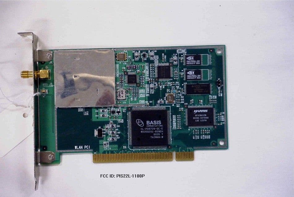
PISWWL-1100P
May 10, 2001Wireless Lan Card
Equipment Class
DSS - Part 15 Spread Spectrum Transmitter
PISWWL-1100N
May 10, 2001Wireless Lan Card
Equipment Class
DSS - Part 15 Spread Spectrum Transmitter