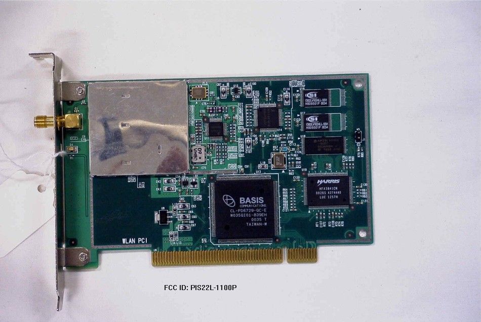
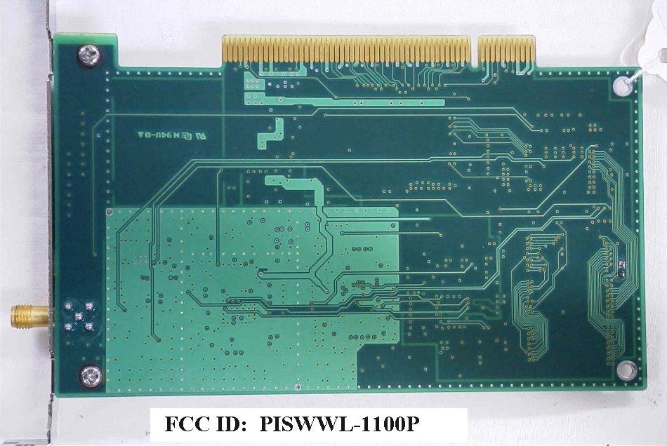
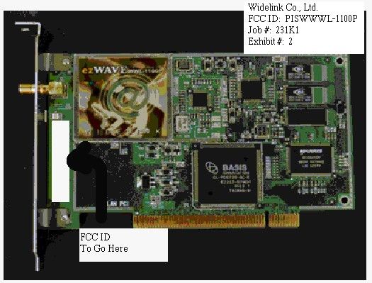
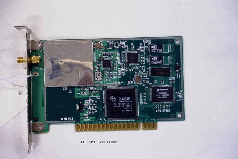
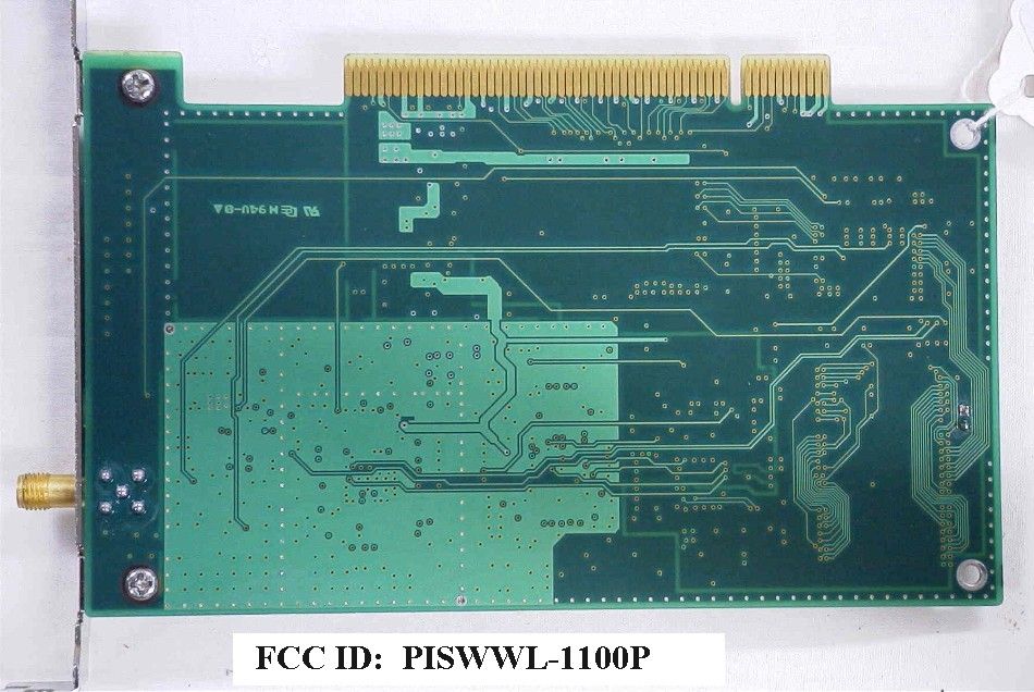
PISWWL-1100PWireless Lan Card
Widelink Co., Ltd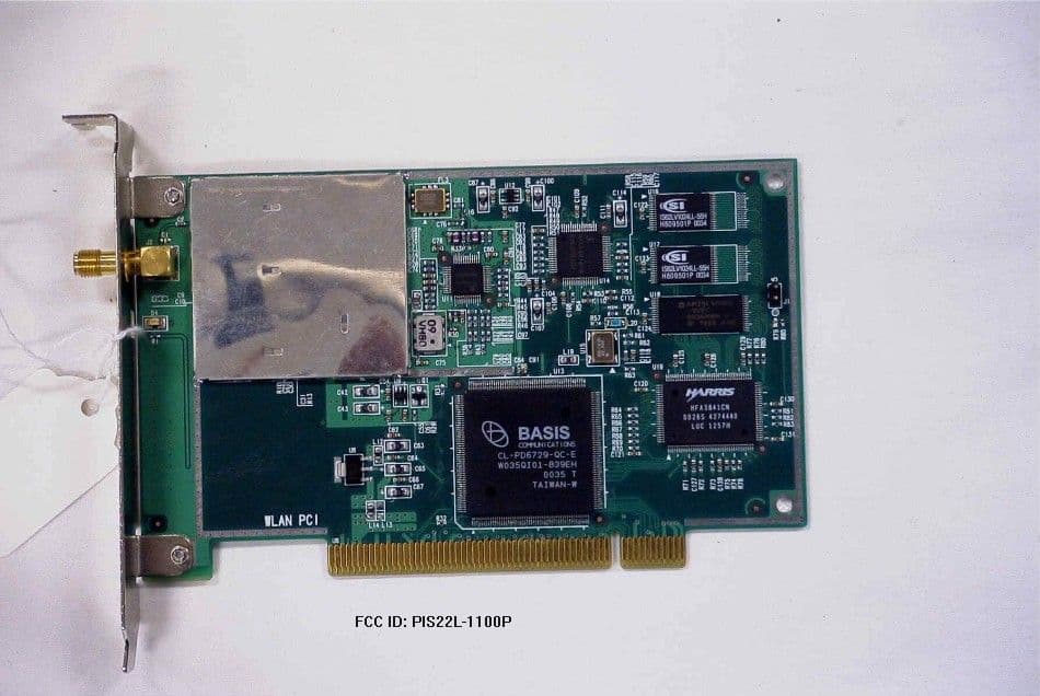
Click to zoom
Application Details
- Equipment Class
- DSS - Part 15 Spread Spectrum Transmitter
- Date of Grant
- May 10, 2001
- Application Purpose
- Original Equipment
- Date of Application
- May 10, 2001
- Equipment Note
- Wireless Lan Card
- Frequency Range
- 2400.00000000 - 2483.50000000
- Company
- Widelink Co., Ltd
- Country
- South Korea
Documents & Files
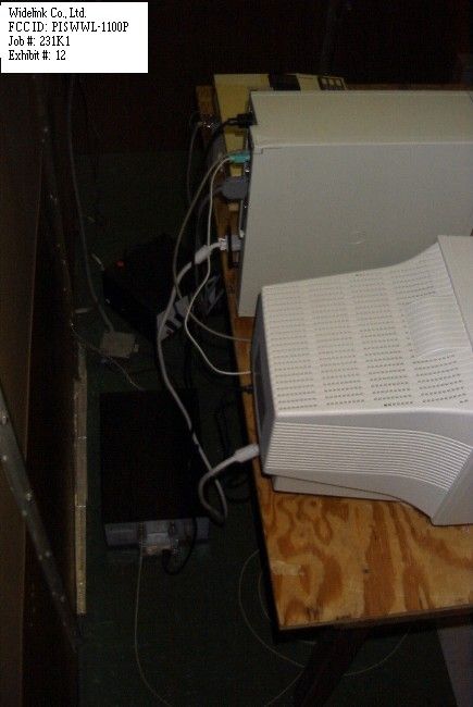
Document Text
Text extracted from the exhibit documents filed with the FCC. Open a document above to read the original.
Users Manual
ezWAVE Cards Users’ GuideVersion 1.6 Copyright© Widelink 2000DOC – 2001.02.01 Page 1 of 36 WWL-1100N&WWL-1100P Wireless LAN Card Users’ Guide Corporate Headquarters Widelink Co. Ltd. 664-25 Dongshin Bldg. 2F Shinsa-Dong, Kangnam-gu Seoul 135-120, Korea http://www.widelink.co.kr Tel:+82-2-3445-9938 Fax:+82-2-3445-8534 ezWAVE Cards Users’ GuideVersion 1.6 Copyright© Widelink 2000DOC – 2001.02.01 Page 2 of 36 Contents Chapter 1Introduction To The Wireless LAN...................... 4 1.1 What is Wireless LAN?.......................................... 4 1.2 Wireless LAN Standard and Structure.............................. 5 Chapter 2Before You Start ezWAVE................................... .10 Chapter 3Installing ezWAVE Card On The Windows Os......11 3.1 Installing PC Card Adapter. ........................................... 11 3.1.1 Installing the PC Card Driver for Windows OS... ... 12 3.1.2 PC Card (PCMCIA) Network Configuration ......... 17 3.1.3 Uninstalling PC Card Software ......................... 21 3.1.4 Remove PC Card from PC card socket ............... 21 3.1.5 ezWAVE Configuration Utility ............................ 22 3.2 PCI Card Installation ..................................................... 26 3.2.1 Installing PCI Card Adapter ............................... 27 3.2.2 Installing PCI Card Driver ..................................29 3.2.3 PCI Card Network Configuration ......................... 29 3.3 Troubleshooting ........................................................... 30 Appendix Appendix ACell Planning (Radio Range)................................... 32 Appendix BTechnical Specification........................................ 34 Appendix CChannel Allocation............................................... 36 ezWAVE Cards Users’ GuideVersion 1.6 Copyright© Widelink 2000DOC – 2001.02.01 Page 3 of 36 THE SPECIFICATIONS AND INFORMATION REGARDING THE PRODUCTS IN THIS MANUAL ARE SUBJECT TO CHANGE WITHOUT NOTICE. ALL STATEMENTS, INFORMATION, AND RECOMMENDATIONS IN THIS MANUAL ARE BELIEVED TO BE ACCURATE BUT ARE PRESENTED WITHOUT WARRANTY OF ANY KIND, EXPRESS OR IMPLIED. USERS MUST TAKE FULL RESPONSIBILITY FOR THEIR APPLICATION OF ANY PRODUCTS. THE SOFTWARE LICENSE AND LIMITED WARRANTY FOR THE ACCOMPANYING PRODUCT ARE SET FORTH IN THE INFORMATION PACKET THAT SHIPPED W ITH THE PRODUCT AND ARE INCORPORATED HEREIN BY THIS REFERENCE.IF YOU ARE UNABLE TO LOCATE THE SOFTWARE LICENSE OR LIMITED WARRANTY, CONTACT YOUR WIDELINK REPRESENTATIVE FOR A COPY. NOTWITHSTANDING ANY OTHER WARRANTY HEREIN, ALL DOCUMENT FILES AND SOFTWARE OF THESE SUPPLIERS ARE PROVIDED “AS IS” WITH ALL FAULTS. WIDELINK AND THE SUPPLIERS DISCLAIM ALL WARRANTIES, EXPRESSED OR IMPLIED, INCLUDING WITHOUT LIMITATION, THOSE OF MERCHANTABILITY, FITNESS FOR A PARTICULAR PURPOSE AND NONINFRINGEMENT OR ARISING FROM A COURSE OF DEALING, USAGE, OR TRADE PRACTICE. IN NO EVENT SHALL WIDELINK OR ITS SUPPLIERS BE LIABLE FOR ANY INDIRECT, SPECIAL, CONSEQUENTIAL, OR INCIDENTAL DAMAGES, INCLUDING WITHOUT LIMITATION, LOST PROFITS OR LOSS DAMAGE TO DATA ARISING OUT OF THE USE OR INABILITY TO USE THIS MANUAL, EVEN IF W IDELINK OR ITS SUPPLIERS HAVE BEEN ADVISED OF THE POSSIBILITY OF SUCH DAMAGES. SAFETY INFORMATION WARNING * Opening the unit, for whatever reason, could lead to damages that are not covered by the guarantee. * To prevent fire or shock hazard, do not expose your ezWAVE wireless LAN PC cards to rain or moisture. NOTES: * The Widelink supplied software may show screens slightly different from those included in this manual. * This manual is written based on the assumption that you are familiar with basic operations of Windows operating system. Microsoft, Windows, Windows95, Windows98, Windows ME, Windows 2000 and Windows NT are registered trademarks of Microsoft Corporation. ezWave, Widellink’s logo, is registered trademark of Widelink Co., Ltd. or its affiliates in Korea, US and certain other countries. All other trademarks mentioned in this documents are the property of their respective owners. The use of word partner does not imply a partnership relationship between Widelink and any of its resellers . Using the Widelink’s ezWAVE card Copyright ⓒ2000. Widelink Co., Ltd. All rights reserved. ezWAVE Cards Users’ GuideVersion 1.6 Copyright© Widelink 2000DOC – 2001.02.01 Page 4 of 36 Chapter 1 Introduction To The Wireless LAN A wireless LAN (WLAN) is a flexible data communication system implemented as an extension to, or as an alternative for, a wired LAN within a building or campus. Using electromagnetic waves, WLANs transmit and receive data over the air, minimizing the need for wired connections. Thus, WLANs combine data connectivity with user mobility, and, through simplified configuration, enable movable LANs. WLANs have gained strong popularity in a number of vertical markets, including the health-care, retail, manufacturing, warehousing, and academic arenas. These industries have profited from the productivity gains of using hand-held terminals and notebook computers to transmit real-time information to centralized hosts for processing. Today WLANs are becoming more widely recognized as a general-purpose connectivity alternative for a broad range of business customers. 1.1What is Wireless LAN? Wireless LANs use electromagnetic airwaves (radio and infrared) to communicate information from one point to another without relying on any physical connection. Radio waves are often referred to as radio carriers because they simply perform the function of delivering energy to a remote receiver. The data being transmitted is superimposed on the radio carrier so that it can be accurately extracted at the receiving end. This is generally referred to as modulation of the carrier by the information being transmitted. Once data is superimposed (modulated) onto the radio carrier, the radio signal occupies more than a single frequency, since the frequency or bit rate of the modulating information adds to the carrier. Multiple radio c…
Text truncated - open the document above for the full version.
Users Manual
Future Communication Leaders – WideLink Co., Ltd. #8-2, Namkyung Bldg. Suite 1001, Samsung-Dong, Kangnam-Gu, Seoul, Korea, 135-090 TEL. 82-2-3445-9938 FAX. 82-2-3445-8534 Send : Widelink Co., Ltd. 2001-05-09 Receive : TIMCO/FCC We will add bellow statements to our user manual. FCC RF Radiation Expoure Statement This equipment complies with FCC RF radiation exposure limits set forth for an uncontrolled environment. This equipment should be installed and operated with a minimum distance of 20 centimeters between the radiator and your body. Important Note : [WWL-1100P/WWL-1100N] Antenna type is unique reverse turn SMA connector, Use only the supplied antenna. Unauthorized antennas, modifications, or attachments could damage the transmitter and may violate FCC regulations. Widelink Co., Ltd. President/CEO Bae Tae Hwa http://www.widelink.co.kr
Users Manual
Future Communication Leaders – WideLink Co., Ltd. #8-2, Namkyung Bldg. Suite 1001, Samsung-Dong, Kangnam-Gu, Seoul, Korea, 135-090 TEL. 82-2-3445-9938 FAX. 82-2-3445-8534 WIDELINK CO., LTD. FCC ID: PISWWL-1100P THE FOLLOWING STATEMENT WILL BE INCLUDED IN OUR USER’S MANUAL. FCC NOTICE This equipment has been tested and found to comply with the limits for a Class B digital device, pursuant to part 15 of the FCC Rules. These limits are designed to provide reasonable protection against harmful interference in a residential installation. This equipment generates, uses and can radiate radio frequency energy and, if not installed and used in accordance with the instructions, may cause harmful interference to radio communication. However, there is no guarantee that interference will not occur in a particular installation. If this equipment does cause harmful interference to radio or television reception, which can be determined by turning the equipment off and on, the user is encouraged to try to correct the interference by one or more of the following measures : - Reorient or relocate the receiving antenna. - Increase the separation between the equipment and receiver. - Connect the equipment into an outlet on a circuit difference from that to which the receiver is connected. - Consult the dealer of an experienced radio/TV technician for help. NOTE : The manufacturer is not responsible for any radio or TV interference caused by unauthorized modifications to this equipment. Such modifications could void the user's authority to operate the equipment. Widelink Co., Ltd. President/CEO Bae Tae Hwa http://www.widelink.co.kr THIS DEVICE COMPLIES WITH PART 15 OF THE FCC RULES. OPERATION IS SUBJECT TO THE FOLLOWING TWO CONDITIONS: (1) THIS DEVICE MAY NOT CAUSE HARMFUL INTERFERENCE, AND (2) THIS DEVICE MUST ACCEPT ANY INTERFERENCE RECEIVED, INCLUDING INTERFERENCE THAT MAY CAUSE UNDERSIRED OPERATION.
ID Label/Location Info
Future Communication Leaders – WideLink Co., Ltd. #8-2, Namkyung Bldg. Suite 1001, Samsung-Dong, Kangnam-Gu, Seoul, Korea, 135-090 TEL. 82-2-3445-9938 FAX. 82-2-3445-8534 FCC ID : PISWWL-1100P ezWAVE MODEL NO : WWL-1100P
Test Report
APPLICANT: WIDELINK CO., LTD. FCC ID: PISWWL-1100P TABLE OF CONTENTS TEST REPORT CONTAINING: PAGE 1.............TEST EQUIPMENT LIST & TEST PROCEDURE PAGE 2.............TEST PROCEDURES CONTD. PAGE 3.............PRODUCT DESCRIPTION PAGE 4.............POWERLINE CONDUCTED INTERFERENCE DATA PAGE 5A-5B.........POWERLINE CONDUCTED PLOTS PAGE 6.............6.0dB BANDWIDTH & POWER OUTPUT PAGE 7.............6.0dB BANDWIDTH PLOT PAGE 8.............METHOD OF MEASURING RF CONDUCTED SPURIOUS EMISSIONS & SPURIOUS EMISSIONS AT ANTENNA TERMINALS PAGE 9.............RADIATION INTERFERENCE TEST DATA PAGE 10............METHOD OF MEASURING RADIATION INTERFERENCE PAGE 11............RADIATED SPURIOUS EMISSIONS INTO ADJACENT RESTRICTED BAND PAGE 12............BANDEDGE PLOT PAGE 13............POWER SPECTRAL DENSITY AND PROCESSING GAIN PAGE 14A-14C......POWER SPECTRAL DENSITY PLOT EXHIBIT ATTACHMENTS: EXHIBIT 1...........FCC ID LABEL SAMPLE EXHIBIT 2...........SKETCH OF FCC ID LABEL LOCATION EXHIBIT 3...........COMPONENT SIDE & SOLDER SIDE PHOTOGRAPHS EXHIBIT 4...........BLOCK DIAGRAM EXHIBIT 5A-5E.......SCHEMATICS EXHIBIT 6A-6F.......CIRCUIT DESCRIPTION EXHIBIT 7A-7F.......PROCESSING GAIN TEST METHODS EXHIBIT 8A-8C.......PROCESSING GAIN DATA EXHIBIT 9...........INSTRUCTION MANUAL EXHIBIT 10-11.......TEST SET UP PHOTO - RADIATED EXHIBIT 12..........TEST SET UP PHOTO - POWERLINE APPLICANT: WIDELINK CO., LTD. FCC ID: PISWWL-1100P REPORT #: T:\CUS\W\WIDECO\231K1\231K1RPT.DOC TABLE OF CONTENTS LIST TEST EQUIPMENT LIST 1._X_Spectrum Analyzer: HP 8566B-Opt 462, S/N 3138A07786, w/ preselector HP 85685A, S/N 3221A01400, Quasi-Peak Adapter HP 8565OA, S/N 3303A01690 & Preamplifier HP 8449B-OPT H02, S/N 3008A00372 Cal. 1/19/01 2._X_Biconnical Antenna: Eaton Model 94455-1, S/N 1057, Cal 3/15/00 3.___Biconnical Antenna: Electro-Metrics Model BIA-25, S/N 1171 Cal. 3/16/01 4._X_Log-Periodic Antenna: Electro-Metrics Model EM-6950, S/N 632 Cal. 3/15/00 5.___Log-Periodic Antenna: Electro-Metrics Model LPA-30, S/N 409 Cal. 3/15/00 6._X_Double-Ridged Horn Antenna: Electro-Metrics Model RGA-180, 1-18 GHz, S/N 2319 7.___18-26.3GHz Systron Donner Standard Gain Horn #DBE-520-20 8.___Horn 40-60GHz: ATM Part #19-443-6R 9.___Line Impedance Stabilization Network: Electro-Metrics Model ANS-25/2, S/N 2604 Cal. 2/9/00 10.___Temperature Chamber: Tenney Engineering Model TTRC, S/N 11717-7 Cal. 1/21/01 11.___Frequency Counter: HP Model 5385A, S/N 3242A07460 Cal 11/20/00 12.___Peak Power Meter: HP Model 8900C, S/N 2131A00545, Cal. 1/26/01 13._X_Open Area Test Site #1-3meters Cal. 12/22/99 14.___Signal Generator: HP 8640B, S/N 2308A21464 Cal. 11/21/00 15.___Signal Generator: HP 8614A, S/N 2015A07428 16.___Passive Loop Antenna: EMCO Model 6512, 9KHz to 30MHz, S/N 9706-1211 Cal. 6/10/00 17.___Dipole Antenna Kit: Electro-Metrics Model TDA-30/1-4, S/N 153 Cal. 11/24/00 18.___AC Voltmeter: HP Model 400FL, S/N 2213A14499 Cal. 2/1/01 19.___Digital Multimeter: Fluke Model 8012A, S/N 4810047 Cal 9/21/99 20.___Digital Multimeter: Fluke Model 77, S/N 43850817 Cal 11/16/00 21.___Oscilloscope: Tektronix Model 2230, S/N 300572 Cal 2/1/01 TEST PROCEDURE GENERAL: This report shall NOT be reproduced except in full without the written approval of TIMCO ENGINEERING, INC. Shielded interface cables were used in all cases except for cables connecting to the telephone line and the power cords. A test program was run which simulated a normal data transmission on a network. POWER LINE CONDUCTED INTERFERENCE: The procedure used was ANSI STAN- DARD C63.4-1992 using a 50uH LISN. Both lines were observed with the UUT transmitting. The bandwidth of the spectrum analyzer was 10kHz with an appropriate sweep speed. The ambient temperature of the UUT was 77°F with a humidity of 53%. APPLICANT: WIDELINK CO., LTD. FCCID: PISWWL-1100P REPORT #: T:\CUS\W\WIDECO\231K1\231K1RPT.DOC PAGE #: 1 TEST PROCEDURES CONTINUED BANDWIDTH 6.0dB: The measurements were made with the spectrum analyzer’s resolution bandwidth(RBW)=1.0MHz and the video bandwidth(VBW) =3.0MHz and the span set as shown on Page 7A. POWER OUTPUT: The RF power output was measured at the antenna feed point using a peak power meter. ANTENNA CONDUCTED EMISSIONS: The RBW=100KHz, VBW=300KHz and the span set to 10.0MHz and the spectrum was scanned from 30MHz to the 10th Harmonic of the fundamental. Above 1.0GHz the resolution bandwidth was 1.0MHz and the VBW = 3.0MHz and the span to 50MHz. RADIATION INTERFERENCE: The test procedure used was ANSI STANDARD C63.4-1992 using a HEWLETT PACKARD spectrum analyzer with a prese- lector. The bandwidth(RBW) of the spectrum analyzer was 100kHz up to 1GHz and 1.0MHz above 1GHz with an appropriate sweep speed. The VBW above 1.0GHz was = 3.0MHz. The analyzer was calibrated in dB above a microvolt at the output of the antenna. The ambient temperature of the UUT was 77oF with a humidity of 53%. APPLICANT: WIDELINK CO., LTD. FCCID: PISWWL-1100P REPORT #: T:\CUS\W\WIDECO\231K1\231K1RPT.DOC PAGE #: 2 PRODUCT DESCRIPTION: This device is a wireless LAN adapter card that provides wireless connection between computers. FREQUENCY RANGE: 2.4-2.4835 GHz SUPPORT BIT RATES: 11 Mbps CCK, 5.5 Mbps CCK, 2 Mbps DQPSK, 1 mPBS dbsk SPREADING: DSSS (Direct Sequence Spread Spectrum) CHIP RATE: 11 Mcps ANTENNA: External 2 dBi Antenna with SMA connector MEDIA ACCESS PROTOCOL: CSMA/CA (Collission Avoidance) with ACK APPLICANT: WIDELINK CO., LTD. FCCID: PISWWL-1100P REPORT #: T:\CUS\W\WIDECO\231K1\231K1RPT.DOC PAGE #: 3 APPLICANT: WIDELINK CO., LTD. FCC ID: PISWWL-1100P NAME OF TEST: POWER LINE CONDUCTED INTERFERENCE RULES PART NUMBER: 15.107(a) REQUIREMENTS: .45 - 30 MHz 250 uV OR 47.96 dBuV TEST PROCEDURE: ANSI STANDARD C63.4-1992. The spectrum was scanned from .45 to 30 MHz. TEST DATA: THE HIGHEST EMISSION READ FOR LINE 1 WAS 35.1uv @ 8.01MHz. THE HIGHEST EMISSION READ FOR LINE 2 WAS 28.5uv @ 8.55MHz. THE GRAPHS IN THE NEXT TWO PAGES REPRESENT THE EMISSIONS TAKEN FOR THIS DEVICE. TEST RESULTS: Both lines were observed. T…
Text truncated - open the document above for the full version.
Test Report
15.247(c) Method of Measuring RF Conducted Spurious Emissions /--------\ |HP | |Spectrum| |Analyzer| |8566B | \--------/ | /-----------\ /-----------------\ | |TRANSMITTER| | 50 OHM RESISTIVE| | | UNDER TEST|------| LOAD |-----\ /-------/ \-----------/ \-----------------/ | | |/-------\| \| |/ \-------/ ATTENUATOR NAME OF TEST: SPURIOUS EMISSIONS AT ANTENNA TERMINALS REQUIREMENTS: Emissions must be at least 20dB down from the highest emission level within the authorized band as measured with a 1 MHz RBW. EMISSION dB BELOW FREQUENCY CARRIER ___MHz___ _________ 2418.0 00.0 4836.0 75.8 7254.0 100.0 9672.0 89.4 12090.0 95.8 2437.0 00.0 4874.0 88.4 7311.0 91.9 9748.0 90.7 12185.0 99.2 2467.0 00.0 4934.0 79.0 7401.0 70.7 9868.0 91.0 12335.0 98.4 NOTE: THE SPECTRUM WAS SCANNED TO THE TENTH HARMONIC. APPLICANT: WIDELINK CO., LTD. FCCID: PISWWL-1100P REPORT #: T:\CUS\W\WIDECO\231K1\231K1RPT.DOC PAGE #: 8 15.247(c),15.205 &15.209(b) Field_strength_of_spurious_emissions: REQUIREMENTS: FIELD STRENGTH FIELD STRENGTH 15.209 of Fundamental: of Harmonics 30 - 88 MHz 40 dBuV/m @3M 88 -216 MHz 43.5 2.4-2.4835 GHz 216 -960 MHz 46.0 127.38 dBuV/m @3m ABOVE 960 MHz 54.0 REQUIREMENTS: Emissions that fall in the restricted bands (15.205) must be less than 54dBuV/m otherwise the spurious and harmonics must be attenuated by at least 20dB. TEST DATA: EMISSION METER COAX FIELD FCC. FREQUENCY READING LOSS ACF STRENGTH LIMIT MARGIN MHz @ 3m dBuV dB dB dBuV/m dB dB ANT. 2417.70 73.70 1.09 29.04 103.84 127.38 23.54 V 4835.40 6.70 1.46 33.94 42.10 54.00 11.90 V 2441.90 73.30 1.10 29.10 103.50 127.38 23.88 V 4883.80 1.20 1.46 33.99 36.66 54.00 17.34 H 2471.90 72.60 1.10 29.18 102.88 127.38 24.50 V METHOD OF MEASUREMENT: The procedure used was ANSI STANDARD C63.4-1992 & the Guidance on Measurements for Direct Sequence Spread Spectrum Systems. Measurements were made at the open field test site of TIMCO ENGINEERING INC. located at 849 N.W. State Road, Newberry, FL 32669. APPLICANT: WIDELINK CO., LTD. FCCID: PISWWL-1100P REPORT #: T:\CUS\W\WIDECO\231K1\231K1RPT.DOC PAGE #: 9 2.993(a)(b) 2.993(a)(b) Continued Field_strength_of_spurious_emissions: Method of Measuring Radiated Spurious Emissions * Tuned, Calibrated Antenna which may be raised from 1-4 Meters above ground and changed in polarization. Equipment placed 80 cm above ground on a rotatable platform. APPLICANT: WIDELINK CO., LTD. FCCID: PISWWL-1100P REPORT #: T:\CUS\W\WIDECO\231K1\231K1RPT.DOC PAGE #: 10 APPLICANT: WIDELINK CO., LTD. FCC ID: PISWWL-1100P NAME OF TEST: RADIATED SPURIOUS EMISSIONS INTO ADJACENT RESTRICTED BAND REQUIREMENTS: Emissions that fall in the restricted bands (15.205). These emissions must be less than or equal to 500 uV/m (54 dBuV/m). TEST PROCEDURE: An in band field strength measurement of the fundamental emissions using the RBW and detector function required by C63.4-2000 and FCC rules. The procedure was repeated with an average detector and a plot made. The calculated field strength in the adjacent restricted band is presented below. -102.60 dBm - from Plot + 29.21 dB - ACF + 1.1 dB - Coax Loss ___________ - 72.99 dBm +107.00 ___________ 34.71 dBuV APPLICANT: WIDELINK CO., LTD. FCCID: PISWWL-1100P REPORT #: T:\CUS\W\WIDECO\231K1\231K1RPT.DOC PAGE #: 11 APPLICANT: WIDELINK CO., LTD. FCC ID: PISWWL-1100P NAME OF TEST: POWER SPECTRAL DENSITY RULES PART NUMBER: 15.247(d) REQUIREMENTS: The peak level measured must be no greater than +8.0dBm. DATA: The plots are on the following pages as exhibits # 14A-14C. The level at 2438.03 MHz . 2417.44 MHz 2472.48 MHz From Plot: - 75.8 dBm -73.20 dBm -74.00 dBm + 20.0 dB ATT +20.00 dB ATT +20.00 dB ATT + 35.0 CF +35.00 CF +35.00 CF Calculation: - 20.8 dBm -18.20 dBm -19.00 dBm NAME OF TEST: PROCESSING GAIN RULES PART NUMBER: 15.247(e) REQUIREMENTS: DATA: The processing gain information supplied by the manufacturer is 10.0dB. See Exhibits 7A-7F and 8A-8C for processing gain test methods and data. APPLICANT: WIDELINK CO., LTD. FCCID: PISWWL-1100P REPORT #: T:\CUS\W\WIDECO\231K1\231K1RPT.DOC PAGE #: 13
Test Report
Copyright© 2001 Widelink Co., Ltd. 01-05-03 1 of 7 Processing Gain of a Direct Sequence Spread Spectrum, FCC CFR 47, Para.15.247(e) Product Name : WWL-1100P FCC Requirements: The Processing gain of a direct sequence system shall be at least 10 dB. The Processing gain shall be determined from the ratio in dB of the signal-to-noise ratio with the system spreading code turned off to the signal to noise ratio with the system spreading code turned on, as measured at the demodulated out of the receiver. Environmental Condition: Room temperature and Humidity : +25 °C and 50% Power Input: DC Power from the computer Test Equipment : NO Equipments Vendor Model Name Description 1 Spectrum Analyzer Agilent HP8595E 9KHz ~ 22 GHz 2 Signal Generator Agilent E4421A 3 Power Meter Agilent HP438A 4 Attenuator 10 dB, 20 dB 5 Step Attenuator Weinschel AE117A-69-11 70 dB 6 Step Attenuator Weinschel AF119A-99-33 99 Db 7 Power Splitter AceTeq. 8 Computer Sambo Dreamsys Method of measurement: Jamming Margin Method The processing gain may be measured using the CW jamming method. Figure1 shows the test configuration. The test consists of stepping a signal generator in 50 KHz increments across the passband of the system. At each point, the generator level required to produce the recommended Bit Error Rate(BER) is recorded. This level is the jammer level. The output power of the transmitting unit is measured at the same point. The Jammer to Signal(J/S) ratio is the calculated. Discard the worst 20% of the J/S data points. The lowest remaining J/S ratio is used when calculating the Process Gain. Theoretical Calculation : The use of 8% FER frame error rate(or PER packet error rate) as a substitute for the recommended BER bit error rate and the ideal signal to noise ratio per symbol(Eb/No) is derived in the attached documents Widelink Co., Ltd. FCC ID: PISWWL-1100P Job #: 231K1 Exhibit #: 7A-7F Copyright© 2001 Widelink Co., Ltd. 01-05-03 2 of 7 Processing Gain Test Set Up Desktop Computer WWL-1100P 10 dB Divide Step Attenuator Step Attenuator Divide 10 dB Transmitt er WWL-1100P Receiver Labtop Computer Signal Generator 6 dB Power Meter HP438A Copyright© 2001 Widelink Co., Ltd. 01-05-03 3 of 7 ♦ Processing Gain Test 1. Test Background and Procedure According to FCC regulations[1], a direct sequence spread spectrum system must have a processing gain, Gp of at least 10 dB. Compliance to this requirement can be shown by demonstrating a relative bit-error-ratio(BER) performance improvement between the case where spread spectrum process(coding, modulation) are engaged relative to the process being bypassed. In some practical systems, the spread spectrum processing cannot simply be bypassed. In these cases, the processing gain can be indirectly measured by a jamming margin test [2]. 2. Theoretical calculations The processing gain is related to the jamming margin as follows [2] Gp=[S/N] output +[J/S]+L system Where BERp reference is the reference bit error ratio with its corresponding theoretical output signal to noise ratio per symbol, (S/N)output, (J/S) is the jamming margin(jamming signal power relative to desired signal power)m, and L System are the system implementation losses. The maximum allowed total system implementation loss is 2 dB. The HFA3861A direct sequence spread spectrum baseband processor uses CCK modulation which is a form of M-ary Orthogonal Keying. The BER performance curve is given by [5]. “The probability of error for generalized M-ary Orthogonal signaling using coherent demodulation is given by: [ PePcQz Eb z dz S N M =−=−−+ − − ∞ − ∫ 111 1 2 212 2 01 0 2 1 2 π η (})] exp{ } This integral cannot be solved in closed form, and numerical integration must be used. This is done in a MATHCAD environment and is Copyright© 2001 Widelink Co., Ltd. 01-05-03 4 of 7 2.11000 byte PER vs. Es/No The reference PER is specified as 8%. The corresponding Es/No(signal to noise ratio per symbol) is 16.4 dB. The Eb/No required to achieve the desired BER with maximum system implementation losses is 18.4 dB. The minimum processing gain is again, 10 dB, Gp Es No J S LdBdB J S dB output system = + +=++ ≥16 42 010.. GpdB J S dB=+ ≥18410. The minimum jammer to signal ratio is as follows: J S dB ≥−84. For the case of the HFA3861A, the bit rates are 1,2,5.5, and 11 Mbps. The corresponding symbol rates are 1,1, 1.375, and 1.375 MSps. The chip rate is always 11 Mcps, so the ratio of chip rate to symbol rate is 11:1 for the 1 and 2 Mbps rates and 8:1 for the 5.5 and 11 Mbps rates. Since the symbol rate to bit rate is less than 10 for the higher rates, we supply the theoretical processing gain calculation for these cases where both spread spectrum processing gain and coding gain are utilized. This is reasonable in that they cannot be speparated in the demodulation process. If a separable FEC coding scheme were used, we would not be comfortable making this assertion. The PER can be related to a BER of 1e-5 on 1000 bye packets. With 8 bits per symbol, the Eb/No of BPSK is 9.6 dB for 1e-5 BER, so therefore the coding gain of CCK over BPSK is 2.2 dB. We add this to the processing gain of 9 dB to get 11.2 dB overall processing gain for the CW jammer test. Taking the calculations above, if the J S dB ≥−84. then the equipment passes the CW jamming test. Copyright© 2001 Widelink Co., Ltd. 01-05-03 5 of 7 ∗ ∗∗ ∗ Test Block Diagram ∗ Test Procedure Obtain the simplex link shown. Perform all independent instrumentation calibrations prior to this procedure. Set operating power levels using fixed and variable attenuators in system to meet the following objectives: Desktop Computer PCI Card(TX Combiner Signal Generator Divide Notebook Computer PCI Card(TX Spectrum Analyzer Copyright© 2001 Widelink Co., Ltd. 01-05-03 6 of 7 1. Signal Power at receiver approximately –50 dBm 2. Signal Power at power meter between –5 and –10 dBm for optimal linearity. 3. Use spectrum analyzer to mon…
Text truncated - open the document above for the full version.
Test Report
Freq.Gp(S/N)oMj=J/SLsysJammerPER (MHz)(dB)(dB)(dB)(dB)(dBm) 2403.520.2916.41.892-48.116.34 2403.720.8516.42.452-47.553.83 2403.921.0516.42.652-47.354.01 2404.120.9816.42.582-47.424.82 2404.320.3916.41.992-48.014.72 2404.519.5916.41.192-48.814.41 2404.719.3816.40.982-49.027.54 2404.919.3016.40.902-49.14.12 2405.119.2916.40.892-49.114.23 2405.319.5816.41.182-48.824.54 2405.519.2016.40.802-49.22.21 2405.718.3816.4-0.022-50.023.02 2405.918.2916.4-0.112-50.115.05 2406.118.5116.40.112-49.893.79 2406.318.0316.4-0.372-50.374.22 2406.517.7716.4-0.632-50.637.5 2406.716.7716.4-1.632-51.637.8 2406.917.2916.4-1.112-51.117.72 2407.117.2916.4-1.112-51.117.51 2407.317.1116.4-1.292-51.297.24 2407.517.3216.4-1.082-51.087.38 2407.716.5416.4-1.862-51.867.29 2407.916.4516.4-1.952-51.957.74 2408.116.4816.4-1.922-51.927.17 2408.316.4416.4-1.962-51.967.91 2408.516.2016.4-2.202-52.27.89 2408.715.7416.4-2.662-52.667.62 2408.916.0216.4-2.382-52.387.45 2409.115.7316.4-2.672-52.677.62 2409.315.5616.4-2.842-52.847.66 2409.515.7816.4-2.622-52.627.48 2409.715.8516.4-2.552-52.557.28 2409.915.4716.4-2.932-52.937.87 2410.115.3516.4-3.052-53.057.84 2410.315.4716.4-2.932-52.937.49 2410.515.3916.4-3.012-53.017.42 2410.715.3716.4-3.032-53.037.89 2410.915.7116.4-2.692-52.697.73 2411.115.7916.4-2.612-52.616.57 2411.316.3716.4-2.032-52.036.44 2411.515.7216.4-2.682-52.686.65 2411.716.1016.4-2.302-52.37.65 11Mbps CHANNEL 1 Processing Gain Gp=(S/N)o + Mj + Lsys Freq.Gp(S/N)oMj=J/SLsysJammerPER (MHz)(dB)(dB)(dB)(dB)(dBm) 11Mbps CHANNEL 1 Processing Gain Gp=(S/N)o + Mj + Lsys 2411.915.8316.4-2.572-52.577.1 2412.116.2016.4-2.202-52.25.71 2412.316.2316.4-2.172-52.177.5 2412.516.6116.4-1.792-51.796.36 2412.716.2716.4-2.132-52.137.24 2412.916.4216.4-1.982-51.987.46 2413.115.9816.4-2.422-52.427.37 2413.316.0216.4-2.382-52.387.32 2413.516.1916.4-2.212-52.217.58 2413.716.5116.4-1.892-51.897.11 2413.916.8316.4-1.572-51.576.71 2414.116.5716.4-1.832-51.837.81 2414.316.3416.4-2.062-52.066.84 2414.516.6116.4-1.792-51.797.56 2414.716.2916.4-2.112-52.117.4 2414.917.0016.4-1.402-51.47.92 2415.116.3816.4-2.022-52.027.35 2415.316.3816.4-2.022-52.026.65 2415.516.6216.4-1.782-51.786.39 2415.716.7916.4-1.612-51.616.48 2415.916.5216.4-1.882-51.886.76 2416.116.6716.4-1.732-51.737.13 2416.316.7316.4-1.672-51.677.04 2416.516.9616.4-1.442-51.446.82 2416.716.8916.4-1.512-51.517.25 2416.916.9616.4-1.442-51.447.2 2417.117.4016.4-1.002-516.97 2417.317.4016.4-1.002-517.84 2417.517.3916.4-1.012-51.017.87 2417.718.0416.4-0.362-50.367.7 2417.918.1416.4-0.262-50.267.87 2418.118.1616.4-0.242-50.246.45 2418.318.2716.4-0.132-50.136.75 2418.518.6116.40.212-49.797.25 2418.719.3416.40.942-49.066.32 2418.919.4616.41.062-48.946.02 2419.119.3716.40.972-49.037.03 2419.318.7416.40.342-49.666.71 2419.526.9316.48.532-41.475.18 2419.720.2116.41.812-48.197.6 2419.920.2616.41.862-48.146.47 2420.120.0916.41.692-48.317.8 Freq.Gp(S/N)oMj=J/SLsysJammerPER (MHz)(dB)(dB)(dB)(dB)(dBm) 11Mbps CHANNEL 1 Processing Gain Gp=(S/N)o + Mj + Lsys 2420.320.1416.41.742-48.267.86 2420.520.6316.42.232-47.777.36 Packet Delay=1, Packet Burst=6 Transmitter Signal Level at Rx= -50 dBm "Mode=11b, Pseudo IBSS" Packet Size= 1000byte Test Conditions AWL-1100P
Contact Information
Applicant
Cho Chang-Yeon(PR Manager)
Test Firm
Timco Engineering, Inc.S Sanders
Technical Specifications
| # | Rule Parts | Frequency Range | Power Output |
|---|---|---|---|
| 1 | 15C | 2.40 GHz - 2.48 GHz | 35.60 mW |
Other Applications from Widelink Co., Ltd
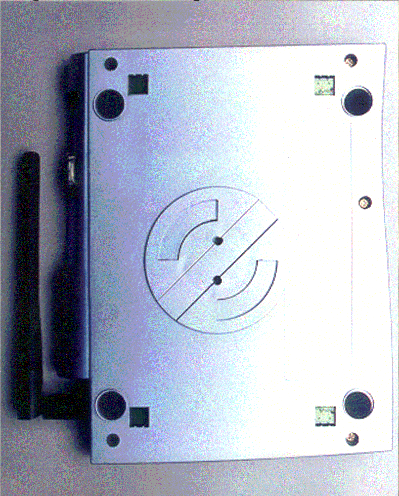
PISWAP-1100E
Jul 05, 20012.4GHz Wireless LAN
Equipment Class
DSS - Part 15 Spread Spectrum Transmitter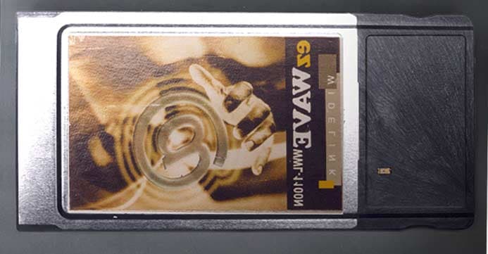
PISWWL-1100N
May 10, 2001Wireless Lan Card
Equipment Class
DSS - Part 15 Spread Spectrum Transmitter