PJDSV-01-TXVideo/ Audio Wireless TX
Strategic Vista (BVI) Ltd.
Click to zoom
Application Details
- Equipment Class
- DXX - Part 15 Low Power Communication Device Transmitter
- Date of Grant
- Apr 16, 2001
- Application Purpose
- Original Equipment
- Date of Application
- Apr 16, 2001
- Equipment Note
- Video/ Audio Wireless TX
- Frequency Range
- 2410.50000000 - 2472.50000000
- Company
- Strategic Vista (BVI) Ltd.
- Country
- Virgin Islands (British)
Documents & Files
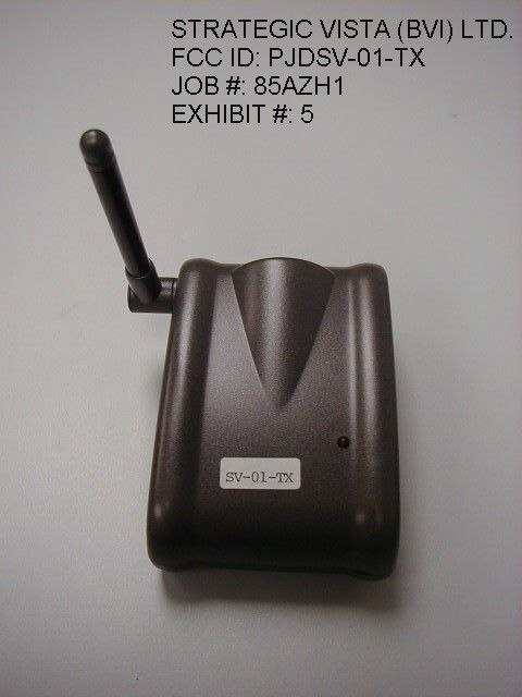
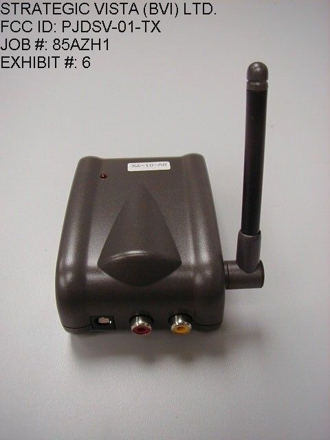
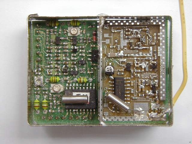
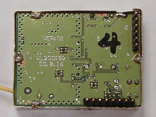
Document Text
Text extracted from the exhibit documents filed with the FCC. Open a document above to read the original.
Users Manual
SV-01-TX 2.4G Video/Audio Wireless Transmitter Important Safety Precautions THIS DEVICE COMPLES WITH PART 15 OF THE FCC RULES. OPERATION IS SUBJECT TO THE FOLLOWING TWO CONDITIONS, (1) THIS DEVICE MAY NOT CAUSE HARMFUL INTERFERENCE AND (2) THIS DEVICE MUST ACCEPT ANY INTERFERENCE RECEIVED, INCLUDING INTERFERENCE THAT MAY CAUSE UNDESIRED OPERATION, NOTE : THE MANUFACTURER IS NOT RESPONSIBLE FOR ANY RADIO OR TV INTERFERENCE CAUSED BY UNAUTHORIZED MODIFICATIONS TO THIS EQUIPMENT. SUCH MODIFICATIONS COULD VOID THE USER’S AUTHORITY TO OPERATE THE EQUIPMENT. Index 1. Introduction 2. Description of Box Contents 3. Connection and Setup 4. Operation 5. Specification FCC ID : PJDSV-01-TX JOB # : 85AZH1 EXHIBIT # : 10 1. Introduction WL2001Tx is an wireless video sender using the most world-wide popular 2.4Ghz ISM band and design with high flexibility make SV-01-TX a very versatile device. It can transmit a wide band composite video and two audio channels signals up to 100 meters. Features : 2. Description of Box Contents - Mini Transmitter main unit X 1 pc - AC adapter X 1 pc 120VAC to 12VDC - Power spilt cable X 1 pc - Mounting screw X 1 pc - Anchor X 1 pc - Warning decals X 2 pcs - Audio/Video RCA cable X 1 pcs 3. Connection and Setup Connectors and switch Switch/Selector 1. Channel selector (CH1 – CH4) 4 way slide switch 2. Power on/off switch 3. Power Indicator Input Jack/Terminal 1. DC input jack 2. RCA Video input jack 3. RCA Audio input jack How to wall mount the Transmitter How to connect your A/V equipment to Transmitter How to connect your camera to Transmitter - use of Y-spilt power cable to share the DC power 4 Operation You can receive A/V signal from the Transmitter on several Receiver in remote location. 1. Be sure to set the power switches on the transmitter and receiver to the OFF position before proceeding with the following steps. 2. Connect all video/Audio cable to the transmitter and receiver. 3. Connect all power source to the transmitter and receiver. 4. Select a channel 1 – 4 on the transmitter 5. Switch on the transmitter and receiver 6. Search the channel 1 – 4 on the receiver using the channel selector switch. ( All receiver and transmitter must have the same channel), you should see the Picture on the receiver. 7. Select another channel on transmitter and receiver if necessary for better picture quality. 8. Adjust the antenna as necessary 5. Specification / Features Power Supply : AC adapter DC 12V 500mA output Current consumption : 150 mA typ. Channel Frequency : 2411 - 2473 Mhz Channel Selection : 4 Channel Modulation System : FM modulation Video Channel : 1 Video Input level : 1Vpp @ 75 Ohm Audio Channel : 1 Audio Input level : 1 Vpp @ 600 Ohm Transmission channel : Video X 1 Audio X 1 Antenna type : Dipole LED indicator : Power Dimensions : 98 X 62 X 40 mm Weight : 98 g
Block Diagram
Antenna 2.4GHz RF TRANSMITTER MODULE U1 PLL frequency synthesizer controller Q5, Q6, Q8 RF Mixer, amp Q1, Q2Q3, Q4U2 MCU controller VIDEO path6 Mhz Audio sub-6.5 Mhz Audio sub- carriercarrier VA1A2 CH1 CH2 CH3 CH4 Channel selector CONTROL BOARD AC/DC INU1 REGULATORPower LED * Optional V INAudio L IN 2.4GHz SV-01-TX Mini Transmitter
ID Label/Location Info
FCC ID label for SV-01-TX FCC ID : PJDSV-01-TX MADE IN CHINA THIS DEVICE COMPLES WITH PART 15 OF THE FCC RULES. OPERATION IS SUBJECT TO THE FOLLOWING TWO CONDITIONS, (1) THIS DEVICE MAY NOT CAUSE HARMFUL INTERFERENCE AND (2) THIS DEVICE MUST ACCEPT ANY INTERFERENCE RECEIVED, INCLUDING INTERFERENCE THAT MAY CAUSE UNDESIRED OPERATION. STRATEGIC VISTA (BVI) LTD. FCC ID: PJD-SV-01-TX JOB #: 85AZH1 EXHIBIT #: 1
ID Label/Location Info
FCC Label Location for SV-01-TX STRATEGIC VISA (BVI) LTD. FCC ID: PJDSV-01-TX JOB #: 85AZH1 EXHIBIT #: 2
Operational Description
Circuit Description for SV-01-TX 2.4G Wireless Transmitter The SV-01-TX is separate into two parts: 1. Transmitter control Portion 2. 2.4G RF transmitter module 1. Transmitter control portion This portion is mainly for power supply circuitry and signal path. The video and audio signal enter the PCB through the RCA connectors and then pass through the control PCB to the 2.4G transmitter module. The power on/off switches on the control PCB control the power supply for the product. The 4 selection slide switch on the control PCB allows user to select the right channel frequency and pass the channel selects information to the RF transmitter module. 2 2.4G RF transmitter module The core of the RF transmitter module is the U1. U1 is a single chip PLL frequency synthesizer. Control data from MCU U2 is entered via the I2C bus, select the oscillator frequency. The output of U1 is feed to control the Q5,Q6 and Q8 which form a RF mixer circuitry. Video signal from control board is passed to the RF mixed. Audio signal A1 is pass to a modulate circuit Q1 and Q2, which modulate the A1 audio signal to a 6Mhz carrier. An optional audio channel A2is pass to a modulate circuitry Q3 and Q4 which modulate the A2 audio signal to a 6.5Mhz carrier. The video signal, together with A1 and A2 signal are entered the RF mixer and through the RF circuitry sent the signal to the dipole antenna to broadcast the signal. STRATEGIC VISTA (BVI) LTD. FCC ID: PJDSV-01-TX EXHIBIT #: 9
Test Report
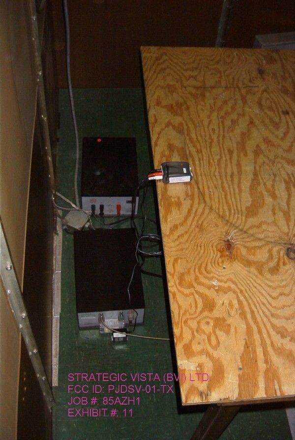
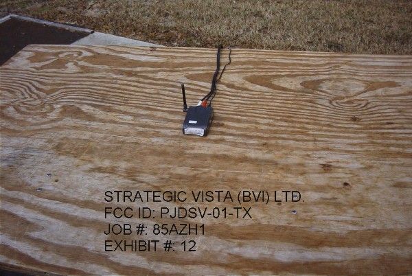
TABLE OF CONTENTS APPLICANT: STRATEGIC VISTA (BVI) LTD. FCC ID: PJDSV-O1-TX TEST REPORT CONTAINING: PAGE 1.............TEST EQUIPMENT LIST & TEST PROCEDURE PAGE 2.............TEST PROCEDURE CONTINUED PAGE 3.............RADIATION INTERFERENCE TEST DATA PAGE 4.............RADIATED SPURIOUS EMISSIONS INTO ADJACENT RESTRICTED BAND PAGE 5.............BANDEDGE PLOT PAGE 6.............OCCUPIED BANDWIDTH PAGE 7.............OCCUPIED BANDWIDTH CW PLOT PAGE 8.............OCCUPIED BANDWIDTH PLOT PAGE 9.............POWERLINE CONDUCTED PAGE 10............POWERLINE PLOT LINE 1 PAGE 11............POWERLINE PLOT LINE 2 EXHIBIT ATTACHMENTS: EXHIBIT 1...........FCC ID LABEL SAMPLE EXHIBIT 2...........SKETCH OF FCC ID LABEL LOCATION EXHIBIT 3...........BLOCK DIAGRAM EXHIBIT 4A-4B.......SCHEMATICS EXHIBIT 5...........FRONT VIEW EXTERNAL PHOTO EXHIBIT 6...........REAR VIEW EXTERNAL PHOTO EXHIBIT 7A-7B.......COMPONENT SIDE INTERNAL PHOTOS EXHIBIT 8A-8B.......COPPER SIDE INTERNAL PHOTOS EXHIBIT 9...........CIRCUIT DESCRIPTION EXHIBIT 10..........USER'S MANUAL EXHIBIT 11..........TEST SET UP PHOTO - POWERLINE CONDUCTED EXHIBIT 12..........TEST SET UP PHOTO - RADIATED EMISSIONS EXHIBIT 13..........SPECIFICATION SHEET APPLICANT: STRATEGIC VISTA (BVI) LTD. FCC ID: PJDSV-O1-TX REPORT #: T:\CUS\S\STRATE\85AZH1\85AZH1.RPT PAGE: TABLE OF CONTENTS LIST APPLICANT: STRATEGIC VISTA (BVI) LTD. FCC ID: PJDSV-O1-TX TEST EQUIPMENT LIST 1._X_Spectrum Analyzer: HP 8566B-Opt 462, S/N 3138A07786, w/ preselector HP 85685A, S/N 3221A01400, Quasi-Peak Adapter HP 8565OA, S/N 3303A01690 & Preamplifier HP 8449B-OPT H02, S/N 3008A00372 Cal. 10/17/99 2._X_Biconnical Antenna: Eaton Model 94455-1, S/N 1057 3.___Biconnical Antenna: Electro-Metrics Model BIA-25, S/N 1171 4._X_Log-Periodic Antenna: Electro-Metrics Model EM-6950, S/N 632 5.___Log-Periodic Antenna: Electro-Metrics Model LPA-30, S/N 409 6._X_Double-Ridged Horn Antenna: Electro-Metrics Model RGA-180, 1-18 GHz, S/N 2319 7.___18-26.3GHz Systron Donner Standard Gain Horn #DBE-520-20 8.___Horn 40-60GHz: ATM Part #19-443-6R 9.___Line Impedance Stabilization Network: Electro-Metrics Model ANS-25/2, S/N 2604 Cal. 2/9/00 10.___Temperature Chamber: Tenney Engineering Model TTRC, S/N 11717-7 11.___Frequency Counter: HP Model 5385A, S/N 3242A07460 Cal 10/6/99 12.___Peak Power Meter: HP Model 8900C, S/N 2131A00545 13._X_Open Area Test Site #1-3meters Cal. 12/22/99 14.___Signal Generator: HP 8640B, S/N 2308A21464 Cal. 9/23/99 15.___Signal Generator: HP 8614A, S/N 2015A07428 16.___Passive Loop Antenna: EMCO Model 6512, 9KHz to 30MHz, S/N 9706-1211 Cal. 6/10/00 17.___Dipole Antenna Kit: Electro-Metrics Model TDA-30/1-4, S/N 153 Cal. 11/24/99 18.___AC Voltmeter: HP Model 400FL, S/N 2213A14499 Cal. 9/21/99 19.___Digital Multimeter: Fluke Model 8012A, S/N 4810047 Cal 9/21/99 20.___Digital Multimeter: Fluke Model 77, S/N 43850817 Cal 9/21/99 21.___Oscilloscope: Tektronix Model 2230, S/N 300572 Cal 9/23/99 TEST PROCEDURE GENERAL: This report shall NOT be reproduced except in full without the written approval of TIMCO ENGINEERING, INC. The UUT was transmit- ting a test signal during the testing. RADIATION INTERFERENCE: The test procedure used was ANSI STANDARD C63.4-1992 using a HEWLETT PACKARD spectrum analyzer with a prese- lector. The analyzer was calibrated in dB above a microvolt at the output of the antenna. The resolution bandwidth was 100KHz and the video bandwidth was 300KHz up to 1.0GHz and 1.0MHz with a video BW of 3.0MHz above 1.0GHz. The ambient temperature of the UUT was 69oF with a humidity of 23%. APPLICANT : STRATEGIC VISTA (BVI) LTD. FCC ID : PJDSV-O1-TX REPORT #: T:\CUS\S\STRATE\85AZH1\85AZH1.RPT PAGE #: 1 APPLICANT : STRATEGIC VISTA (BVI) LTD. FCC ID : PJDSV-O1-TX TEST PROCEDURE CONTINUED FORMULA OF CONVERSION FACTORS: The Field Strength at 3m was estab- lished by adding the meter reading of the spectrum analyzer (which is set to read in units of dBuV) to the antenna correction factor sup- plied by the antenna manufacturer. The antenna correction factors are stated in terms of dB. The gain of the Preselector was accounted for in the Spectrum Analyzer Meter Reading. Example: Freq (MHz) METER READING + ACF = FS 33 20 dBuV + 10.36 dB = 30.36 dBuV/m @ 3m POWER LINE CONDUCTED INTERFERENCE: The procedure used was ANSI STAN- DARD C63.4-1992 using a 50uH LISN. Both lines were observed. The bandwidth of the spectrum analyzer was 10kHz with an appro- priate sweep speed. The ambient temperature of the UUT was 77oF with a humidity of 52%. ANSI STANDARD C63.4-1992 10.1.7 MEASUREMENT PROCEDURES: The UUT was placed on a table 80 cm high and with dimensions of 1m by 1.5m. The UUT was placed in the center of the table (1.5m side). The table used for radiated measurements is capable of continuous rotation. When an emission was found, the table was rotated to produce the maximum signal strength. At this point, the antenna was raised and lowered from 1m to 4m. The antenna was placed in both the horizontal and vertical planes. The situation was similar for the conducted measurement except that the table did not rotate. The EUT was setup as described in ANSIC63.4-1992 with the EUT 40 cm from the vertical ground wall. APPLICANT : STRATEGIC VISTA (BVI) LTD. FCCID : PJDSV-O1-TX REPORT #: T:\CUS\S\STRATE\85AZH1\85AZH1.RPT PAGE #: 2 APPLICANT: STRATEGIC VISTA (BVI) LTD. FCC ID: PJDSV-O1-TX NAME OF TEST: RADIATION INTERFERENCE RULES PART NUMBER: 15.249, 15.209 REQUIREMENTS: FIELD STRENGTH FIELD STRENGTH S15.209 of Fundamental: of Harmonics 30 - 88 MHz 40 dBuV/m @3M 902-928 MHZ 88 -216 MHz 43.5 2.4-2.4835 GHz 216 -960 MHz 46 94 dBuV/m @3m 54 dBuV/m @3m ABOVE 960 MHz 54dBuV/m EMISSIONS RADIATED OUTSIDE OF THE SPECIFIED FREQUENCY BANDS, EXCEPT FOR HARMONICS, SHALL BE ATTENUATED BY AT LEAST 50 dB BELOW THE LEVEL OF THE FUNDAMENTAL OR TO THE GENERAL RADIATED EMISSION LIMITS IN 15.209, WHICHEVER IS THE LESSER ATTENUATION. TEST RESULTS: This unit DOES meet the FCC requirements. TEST DATA: EMISSION METER READING COAX…
Text truncated - open the document above for the full version.
Contact Information
Applicant
Joel Kligman(President)
Test Firm
Timco Engineering, Inc.S Sanders
Technical Specifications
| # | Rule Parts | Frequency Range | Power Output |
|---|---|---|---|
| 1 | 15C | 2.41 GHz - 2.47 GHz | - |
Other Applications from Strategic Vista (BVI) Ltd.

PJDSV-01-CAM
Apr 05, 20012.4GHz Wireless RF Transmitter
Equipment Class
DXX - Part 15 Low Power Communication Device Transmitter