PM9-GMRS1GMRS TRANSCEIVER
ASE Telecom Co Ltd
Click to zoom
Application Details
- Equipment Class
- TNF - Licensed Non-Broadcast Transmitter Held to Face
- Date of Grant
- Jul 25, 2001
- Application Purpose
- Original Equipment
- Date of Application
- May 30, 2001
- Equipment Note
- GMRS TRANSCEIVER
- Frequency Range
- 462.56250000 - 462.72500000
- Company
- ASE Telecom Co Ltd
- Country
- South Korea
Documents & Files
Document Text
Text extracted from the exhibit documents filed with the FCC. Open a document above to read the original.
Users Manual
6. Safety Information Safety Information For GMRS UNIT Your wireless handheld portable transceiver contains a low power(2watts) transmitter. When the Push-to Talk(PTT) button is pushed it sends out radio frequency(RF) signals. This device is authorized to operate at a duty factor not to exceed 50%. In August 1996, the Federal Communications Commission(FCC) adopted RF exposure guidelines with safety levels for hand-held wireless devices. Important Note: To maintain compliance with the FCC's RF exposure guidelines, hold the transmitter and antenna at least 1 inch(2.5 centimeters) from your face and speak in a normal voice, with the antenna pointed up and away from the face. If you wear the handset on your body while using the headset accessory, use only the manufacturers supplied belt clip for this product and ensure that the antenna is at least 1 inch(2.5 centimeters)from your body when transmitting. Use only the supplied antenna. Unauthorized antennas, modifications, or attachments could damage the transmitter and may violate FCC regulations. THIS DEVICE COMPLIES WITH PART 15 OF THE FCC RULES. OPERATION IS SUBJECT TO THE FOLLOWING TWO CONDITIONS: (1) THIS DEVICE MAY NOT CAUSE HARMFUL INTERFERENCE, AND (2) THIS DEVICE MUST ACCEPT ANY INTERFERENCE RECEIVED, INCLUDING INTERFERENCE THAT MAY CAUSE UNDESIRED OPERATION. 7. Instruction Manual 1) General a) General This equipment, GMRS is called 2 way portable handheld radios. The frequency range is 462.5625 462.725MHz, UHF operating channels for International 2 way portable radios. b) Characteristic a. All active device in this radio is composed of semiconductor and high density IC. b. To design this radio in compact and weight approximately 140g including battery. c. CPU of this equipment is HD3802 from HITACHI. d. It's power can operate by use of alcaline 4 cell(1.5V AA) battery. c) Composition This radio is composed of following. a. Transmitter(W/Antenna) b. Belt clip c. Ni-MH battery(option) 2) Specification a) General Specification a. Frequency Range : 462.5625 462.725 MHz b. Output Impedance : 50ÙUnbalanced c. Modulation Type : 8K0F3E d. Communication Mode : Half duplex e. Channel Capacity : 15 channel f. Channel spacing : 12.5 KHz g. Power : 6.0V(alkaline) h. Battery Life : ALCA.2600mAh >40 hours (Tx5%, Rx5%, Stand-by 90%) i. Operating Temperature : -20 +60 j. Dimension : 95.5(H)x 50(W)x 26(D)mm k. Weight : 140g(with Battery) b) Electrical Specification a. Transmitter 1. Output power : Max. 2.0W 2. Frequency Stability : ±2.5 ppm(-20 +60 ) 3. Modulation Method : FM 4. Oscillation Method : PLL SYNTHESIZER 5. Max. Frequency Deviation : < ±2.5 KHz (with tone) 6. Cooling Method : air-cooling Method 7. Spurious Emission : < 60dB 8. FM Hum/Noise : > -40dB(1kHz 60% modulation,w/CCITT) 9. Distortion : < 5% (1kHz 60% modulation) 10. Tx Audio Response : 6dB /OCT ±3dB PRE- EMPHASIS(300Hz 2.5kHz) b. Receiver 1. Receive Method : Double Super Heterodyne 2. Receive Sensitivity : < 0.28uV(20dB SINAD w/CCITT) 3. Squelch Sensitivity : 6 8dB(12dB SINAD) 4. Bandwidth : > 3kHz(6dB ATT point) 5. Selectivity : < -60dB(12.5kHz) 6. Local Frequency Stability : ±2.5ppm(-20 +60 ) 7. Spurious Response : > 40dB 8. Audio output : 200mW(Internal 8Ù load THD 10%) Ext.100mW 9. Distortion : < 5% (1kHz 60% Modulation) 10. RX Audio Response : 6dB/OCT ±3dB DE-EMPHASIS(300Hz 2.5kHz) 11. S/N Ratio : < 40dB(1kHz 60% modulation w/CCITT) 12. IF : 1'st IF = 21.7MHz 2'nd IF = 450kHz 13. Local Frequency : 1st Local Frequency = fc - 21.7MHz 2nd Local Frequency = 21.25MHz 3) Operation a) Key Name a. Function and Controls 1. External Mic/Speaker/CHG 2. Antenna 3. Power On/Off Volume 4. Detachable Belt Clip 5. Push-To-Talk (PTT) Button 6. Monitor/Lamp Button 7. TX Power Hi/Low Button 8. Menu Button 9. EMG/Call Button 10. Up Button 11. Down Button 12. Built-in Microphone 13. Built-in Speaker 14. Battery Cover 15. Charge Terminal b) Icons on LCD a. RSSI (Receiving Signal Strength Indicator) or TX Bar Icon Indicates the receiving signal strength and Full range of signal during transmission. b. Monitor or Lamp Indicator Appears busy icon when the monitor button is long(about 0.5 sec.) used. Short press the Mon button and would be emitting the backlight lamp during 5 seconds. c. CTCSS Indicator Tone digits blink before when the select CTCSS tone CH. d. Auto Channel Scan Indicator SCAN icon appears in the auto scan mode or when the auto scan mode is activated. e. Key Lock Indicator Blinks in auto lock selection mode or when the key lock is activated. f. VOX Indicator VOX icon blinks in VOX selection mode or appears when VOX is activated. g. Battery Level Indicator Battery Level Meter indicates the remaining battery strength. h. Power Save Display P/SAVE icon blinks when the power save is activated. the rate at which the icon blinks varies with the power saving ratio. i. Tx Indicator TX LED lamp emitting when a signal is being transmitted. j. Rx Indicator Appears and RX LED emitting green color when a signal is being received. k. EMG/CALL indicator Short press EMG/CALL button, would be change CH 10 and EMG icon appears. Long press EMG/CALL button(longer 0.5 second), would be call beep transmission and CALL icon appears. l. Hi/Lo indicator When use Hi/Lo power wanted power state. m. Large Segment Display Indicates the channel number in use at the normal mode. When the Function Button is pressed. n. Small Segment Display Displays the CTCSS tone option at the normal mode. o. Roger beep Segment Display ROGER icon appears when the Roger beep activate. c) Key Function a. Power Volume - When power is on, briefly to turn the unit on. A short confirming melody will play. b. Menu button - Press this button briefly to enter function edit mode in standby mode. c. Up/Dn button - In the function edit mode, press briefly to shift from the current option in each sub-menu to the next option in the same sub menu. d. Push-to-Talk (PTT) button - Press it firmly and speak into the Built-in Microphone to transm…
Text truncated - open the document above for the full version.
Cover Letter(s)
TIMCO ENGINEERING, INC. P.O. BOX 370 849 N.W. STATE ROAD 45 NEWBERRY, FL 32669 PHONE: 888-472-2424 OR 352-472-5500 FAX: 352-472-2030 EMAIL: [email protected] July 19, 2001 Frank Coperich Federal Communications Commission Authorization and Evaluation Division 7435 Oakland Mills Road Columbia, MD 21046 Ref: ASE TELECOM CO., LTD.’S FCC ID: PM9-GMRS1 CONFIRMATION #: EA101190, YOUR CORRESPONDENCE ID 19861 Dear Mr. Coperich: With reference to your request of 7/5/01; 1. On the 731 form, the frequency tolerance should have been listed as 5 ppm. Please correct it. 2. The output power has been corrected in the user’s manual and uploaded to the file. 3. I’ve uploaded a list of channels. 4. I’ve uploaded a new audio low pass filter plot. Should you have any questions or require any further information, please advise. Regards, Sharon A. Hoffman TIMCO ENGINEERING, INC.
External Photos
1) Side View 2) Rear View
ID Label/Location Info
PM9-GMRS1
ID Label/Location Info
FCC ID Label To Go Here
Internal Photos
3) Top PCB View 5) Bottom PCB View
Operational Description
9. Circuit Description 1) Frequency synthesizer Frequency synthesizer consists of VCO, PLL IC(built in Prescaler) and loop filter. a) VCO VCO is composed of one VCO. Oscillation circuit takes colpitts circuit using variable Diode. And VCO is composed of D202,Q202,C203,205,206,207,L202. VCO control voltage through loop filter adjusts frequency and Microphone signal through Modulation terminal makes modulation. b) PLL IC PLL IC is adjustable IC to produce the wished frequency which VCO provides through loop filter. It has internal counter using 21.25MHz reference frequency to make 6.25kHz as reference Signal. VCO frequency from prescaled input is divided signal is compared with Reference signal phase in phase comparator. Built-in charger pump changes voltage (until two signals are in phase) and charged voltage supplies VCO through loop filter to produce the desired frequency. Frequency data associated with channel goes to PLL IC by CPU through CLOCK, DATA. PLL IC enables by strobe line of CPU. c) Loop Filter Loop filter is composed of R221,220,C240,238,237 and changes pulse from pin3 to DC., and eliminates harmonic component in pulse. It helps VCO oscillate clearly as DC voltage is supplied into Varicap. 2) Receiver This is composed of Dual Conversion Super Heterodyne. First IF is 21.7MHz. Local oscillator frequency is lower in 1'st IF than Rx frequency. It is called low side injection. Second IF is 450kHz. 2nd local oscillator frequency comes to 21.25MHz. a) Rx/Tx Conversion Circuit Rx signal goes to Rx/Tx conversion circuit through FIXED antenna connector, low pass filter(L310,311,312,C314,318,320,321,) and receiver resonance circuit composed of L313,C102. When transmitting, voltage through R311,L308,D301 supplies,D301 of receive input is short and Tx is on condition. When PIN diode is off in condition of Rx, L313 and C102 resonate serially and make impedance matching at receiver band-pass filter. (CF1). b) Front End Front-End has Q101 to provide a high sensitivity and low noise feature. It employs Saw filter as band pass filter to eliminate image frequency and to produce enough pass band by Q101 input and output. c) Mixer Mixer has one base 2SC4901(Q102) to feature high low noise quality. It has RF signal through C218, CF101 and Q101 RF signal from Local oscillator mixed. It develops 1'st IF ,21.7MHz. 1st IF goes to 1st IF amplifier Q3(KTC3880) base through X-tal filter CF102. IF of mixing signals is selected and taken into X-tal filter. Output impedance of mixer is direct matched with input impedance of X-tal filter. Matching of filter satisfies pass bandwidth of filter, ripple elimination with in pass band, and attenuation characteristic of stop band. X-tal filter is composed of two pole monolithic X-tal filter, 8 kHz of IF bandwidth R113 is used as impedance matching with 1'st IF Amp Q3. d) IF AMP and Detection 1'st IF AMP Q103 supplies IF(IC101) mixer input pin16 through output resistor R122 and C128 to need gain in insertion loss of X-tal filter and last stage circuit. Multi-use IF IC makes up of mixer IF AMP. pin1 2'nd local frequency enter to pin1. It supplies mixer of internal IC. Mixer output of IC through pin3 passes 450kHz ceramic filter, supplies 2'nd IF amplifier and limits. After 2'nd IF AMP has a process of enough gain and AM rejection, it comes to quadrature detection. Demodulated audio signal by L108 (Quad Coil) is amplified and comes out to pin9. Detected audio signal through R140,IC102A/C, VR101 and input in audio amp. IC103 through C151. e) Squelch Circuit Noise component of detected outputs has amplification Squelch threshold is controlled by Resistor R123,R125 f) Audio Amplifier Demodulated audio signal enters to pin2 of IC103. After above signal amplies in IC103 pin5 through C156. It comes out to pin5 Then, It reaches at speaker. 3) Transmitter When Tx develops with pressing PTT switch, VCO output amplifies through Q302,303 transmits by antenna through low pass filter. Tx RF signal produced from Tx VCO is amplified by Driver Q302 through C306 and entered Q303 Power TR input terminal with final amplification. After this stage, the signal is emitted at antenna through 50Ùmatching circuit to low pass filter(L310,311,312,C314,C318,320,321)to eliminate harmonic. a) Audio Modulation and Audio Amplification Audio signal produced by external or internal microphone, limits amplification by IC503.. It enters to VCO through low pass filter and IC503B. Max. Frequency modulation deviation is adjusted by RV201 keeps noise and audio from entering to VCO at time of Tx. Audio modulation and Audio Amplification has characteristic of 6dB/OCT pre-emphasis by IC503D(KIA324).
Operational Description
6) Channel Data ( Unit: MHz) Channel TX Frequency1st Local 1462.5625440.8625 2462.5875440.8875 3462.6125440.9125 4462.6375440.9375 5462.6625440.9625 6462.6875440.9875 7462.7125441.0125 8462.5750440.8750 9462.6250440.9250 10462.6750440.9750 11462.5500440.8500 12462.6000440.9000 13462.6500440.9500 14462.7000441.0000 15462.7250441.0250
Test Report
TABLE OF CONTENTS LIST APPLICANT: ASE TELECOM CO., LTD. FCC ID: PM9-GMRS1 TEST REPORT: PAGE 1......COVER SHEET - GENERAL INFORMATION & TECHNICAL DESCR. PAGE 2......TECHNICAL DESCRIPTION CONTINUED & RF POWER OUTPUT PAGE 3......MODULATION CHARACTERISTICS & OCCUPIED BANDWIDTH PAGE 4......SPURIOUS EMISSIONS AT ANTENNA TERMINALS PAGE 5......UNWANTED RADIATION PAGE 6......METHOD OF MEASURING SPURIOUS EMISSIONS PAGE 7......FREQUENCY STABILITY PAGE 8......LIST OF TEST EQUIPMENT EXHIBITS CONTAINING: EXHIBIT 1.........FCC ID LABEL SAMPLE EXHIBIT 2.........SKETCH OF LOCATION EXHIBIT 3A........EXTERNAL FRONT VIEW PHOTOGRAPH EXHIBIT 3B........EXTERNAL SIDE VIEW PHOTOGRAPH EXHIBIT 3C........EXTERNAL BACK VIEW PHOTOGRAPH EXHIBIT 3D........INTERNAL COMPONENT VIEW PHOTOGRAPH EXHIBIT 3E........INTERNAL COPPER VIEW PHOTOGRAPH EXHIBIT 4.........BLOCK DIAGRAM EXHIBIT 5.........SCHEMATICS EXHIBIT 6A-6L.....USER'S MANUAL EXHIBIT 7A-7C.....CIRCUIT DESCRIPTION EXHIBIT 8.........AUDIO LOW PASS FILTER EXHIBIT 9.........AUDIO FREQUENCY RESPONSE EXHIBIT 10A.......MODULATION LIMITING 300 Hz EXHIBIT 10B.......MODULATION LIMITING 1000 Hz EXHIBIT 10C.......MODULATION LIMITING 3000 Hz EXHIBIT 11........OCCUPIED BANDWIDTH CW PLOT EXHIBIT 12........OCCUPIED BANDWIDTH EXHIBIT 13........TEST SET UP PHOTO APPLICANT: ASE TELECOM CO., LTD. FCC ID: PM9-GMRS1 DATE: FEBRUARY 23, 2001 REPORT #: A\ASE\449ZAK1\449ZAK1RPT.DOC PAGE: TABLE OF CONTENTS GENERAL INFORMATION REQUIRED FOR CERTIFICATION 2.1033(c)(1)(2) ASE TELECOM CO., LTD. will manufacture the FCCID: PM9-GMRS1 GMRS CHANNELS TRANSCEIVER in quantity, for use under FCC RULES PART 95. ASE TELECOM CO., LTD. 7F., YUNGCHANG B/D., 250 CHEOLSAN-DONG KWANGMYONG-CITY KYUNGGI-DO KOREA 2.1033 (c) TECHNICAL DESCRIPTION 2.1033(c)(3) Instruction book. A draft copy of the instruction manual is included as EXHIBIT 6A-6L. 2.1033(c) (4) Type of Emission: 9K5F3E 95.629 Bn = 2M + 2DK M = 3000 D = 1.75K Bn = 2(3.0)+2(1.75) = 9.5K Authorized Bandwidth 20.0KHz 2.1033(c)(5) Frequency Range: 462.5625 - 462.7250 MHz 95.627 2.10311c)(6)(7) The Maximum Output Power Rating: High: 1.1 Watts Low: 0.1 Watt effective radiated power. 2.1033(c)(8) DC Voltages and Current into Final Amplifier: FINAL AMPLIFIER ONLY FOR LOW POWER SETTING INPUT POWER: (6.0V)(.125A) = .75 Watts FOR HIGH POWER SETTING INPUT POWER: (6.0V)(.70A) = 4.20 Watts 2.1033(c)(9) Tune-up procedure. The tune-up procedure is included in the users manual. APPLICANT: ASE TELECOM CO., LTD. FCC ID: PM9-GMRS1 DATE: FEBRUARY 23, 2001 REPORT #: A\ASE\449ZAK1\449ZAK1RPT.DOC PAGE #: 1 2.1033(c)(10) Complete Circuit Diagrams: The circuit diagram is included as EXHIBIT 5 of this report. The block diagram are included as EXHIBIT 4 of this report. 2.1033(c)(11) A photograph or a drawing of the equipment identification label is included as exhibit No. 1. 2.1033(c)(12) Photographs(8"X10") of the equipment of sufficient clarity to reveal equipment construction and layout, including meters, labels for controls, including any view under shields. See exhibits 3A-3E. 2.1033(c)(13) Digital modulation is not allowed. 2.1033(c)(14) The data required by 2.1046 through 2.1057 is submitted below. 95.639 Power Output shall not exceed 50.0 Watts effective radiated power. There can be no provisions for 95.649 increasing the power or varying the power.RF power output. 2.1046(a) RF power is measured by connecting a 50 ohm, resistive watt meter to the RF output connector. With a nominal battery voltage of 6.0 V, and the transmitter properly adjusted the RF output measures: OUTPUT POWER: HIGH: 1.1 Watts LOW: 0.1 Watt 2.1046(a) RF power output. The test procedure used was TIA/EIA-603 S2.2.1. APPLICANT: ASE TELECOM CO., LTD. FCC ID: PM9-GMRS1 DATE: FEBRUARY 23, 2001 REPORT #: A\ASE\449ZAK1\449ZAK1RPT.DOC PAGE #: 2 2.1047(a)(b) Modulation characteristics: AUDIO FREQUENCY RESPONSE The audio frequency response was measured in ac- cordance with TIA/EIA Specification 603. The audio signal was fed into a dummy microphone circuit and into the microphone connector. The input required to produce 30 percent modulation level was measured. See Exhibit 9. 2.1047(b) Audio input versus modulation The audio input level needed for a particular per- percentage of modulation was measured in accor- dance with TIA/EIA Specification 603. The audio input curves versus modulation are on the following pages. Curves are provided for audio input frequen- cies of 300, 1000, and 3000 Hz. See Exhibits 10A-10C. 95.637 Post Limiter Filter Each GMRS transmitter, except a mobile station transmitter with a power of 2.5Watts or less, must be equipped with an audio low pass filter. At any frequency between 3 & 20KHz the filter must have an attenuation of 60log (f/3) greater than the attenuation at 1KHz. See Exhibit 8. 2.1049 Occupied bandwidth: 95.635(b)(1)(3)(7) At least 25dB on any frequency removed from the center of the authorized bandwidth by more than 50%up to and including 100% of the authorized bandwidth. At least 35 dB on any frequency removed from the center of the authorized BW by more than 100% up to and including 250% of the authorized BW. At least 43+log10(T) on any frequency removed from the center of the authorized bandwidth by more than 250%. REPORT #: A\ASE\449ZAK1\449ZAK1RPT.DOC PAGE #: 3 Method of Measuring Conducted Spurious Emissions 2.1051 Spurious emissions at the Antenna Terminals NAME OF TEST: SPURIOUS EMISSIONS AT ANTENNA TERMINALS REQUIREMENTS: Emissions must be 43 +10log(Po) dB below the mean power output of the transmitter. TEST RESULTS: No antenna conducted is necessary since this unit has a fixed antenna. APPLICANT: ASE TELECOM CO., LTD. FCC ID: PM9-GMRS1 DATE: FEBRUARY 23, 2001 REPORT #: A\ASE\449ZAK1\449ZAK1RPT.DOC PAGE #: 4 2.1053 UNWANTED RADIATION: 95.635(b)(7) The tabulated Data shows the results of the radiated field strength emissions test. The spectrum was scanned from 30 to at least the 10th harmonic of the fundamental. This test was conducted per ANSI C63.4-1992. REQUIREMENT…
Text truncated - open the document above for the full version.
Contact Information
Applicant
J H Kim(Manager)
Technical Contact
Timco Engineering, Inc.Mario R de Aranzeta
[email protected]352-472-5500
849 NW State Road 45 · Newberry, Florida · United States
Non-Technical Contact
Timco Engineering, Inc.Sharon A Hoffman
[email protected]352-472-5500
Test Firm
Timco Engineering, Inc.S Sanders
Technical Specifications
| # | Rule Parts | Frequency Range | Power Output | Emission | Tolerance |
|---|---|---|---|---|---|
| 2 | 95A | 462.5625 MHz - 462.725 MHz | 100.00 mW | 9K50F3E | 0.0005 % |
Other Applications from ASE Telecom Co Ltd
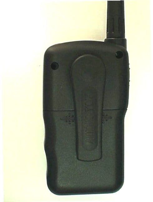
PM9GMRS1600
Aug 01, 2002FRS/GMRS Combination Transceiver
Equipment Class
FRF - Part 95 Family Radio Face Held Transmitter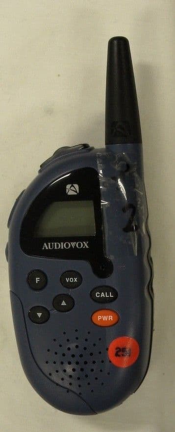
PM9FR548
Jul 11, 2002FRS
Equipment Class
FRF - Part 95 Family Radio Face Held Transmitter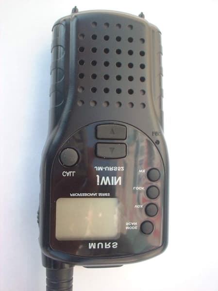
PM9MURS2
Apr 30, 2002MURS Transceiver TX Portion
Equipment Class
TNF - Licensed Non-Broadcast Transmitter Held to Face