Q4I0008837940DESCRIPTION OF PRODUCT AS IT IT MARKED
Elutions, Inc.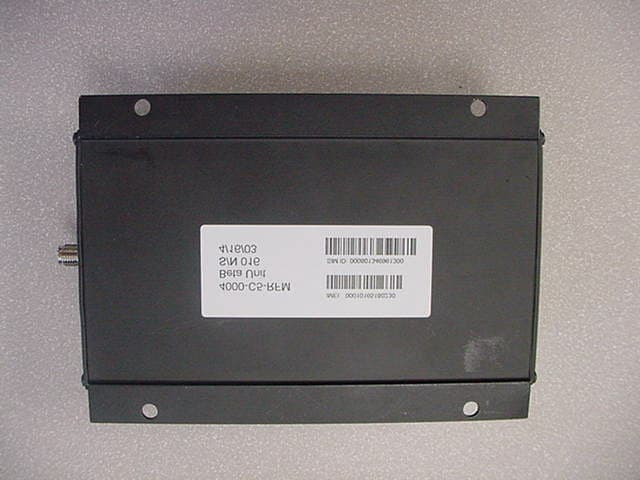
Click to zoom
Application Details
- Equipment Class
- TNB - Licensed Non-Broadcast Station Transmitter
- Date of Grant
- Jul 07, 2003
- Application Purpose
- Original Equipment
- Date of Application
- Jul 07, 2003
- Equipment Note
- DESCRIPTION OF PRODUCT AS IT IT MARKED
- Frequency Range
- 896.00000000 - 901.00000000
- Company
- Elutions, Inc.
- Country
- United States
Documents & Files
Document Text
Text extracted from the exhibit documents filed with the FCC. Open a document above to read the original.
Users Manual
iR1200 Data Modem Installation Guide Draft Version 1.1 April 17, 2003 Table of Contents 2 Table of Contents Table of Contents...............................................................................................................2 Safety Notice.......................................................................................................................5 Safe and Efficient Operation Guidelines.........................................................................5 Exposure to Radio Frequency Energy.............................................................................5 Medical and Personal Electronic Devices.......................................................................5 Pacemakers......................................................................................................................5 Hearing Aids....................................................................................................................5 Other Medical Devices....................................................................................................6 Interference to Other Electronic Devices........................................................................6 FCC Regulation.................................................................................................................7 Introduction........................................................................................................................8 Welcome to Nextel iR1200 Data Modem......................................................................8 Using This Guide.........................................................................................................8 Nextel Coverage........................................................................................................8 Nextel Customer Care...............................................................................................8 Overview...........................................................................................................................10 General Overview..........................................................................................................10 Modem Operating Modes..............................................................................................12 Installation Procedures...................................................................................................13 Before You Start Installing............................................................................................13 Installation Tools.......................................................................................................13 Vehicle Installation..........................................................................................................14 iR1200 3 Mounting the Modem....................................................................................................14 Antenna Mounting.........................................................................................................15 Antenna Installation Considerations.........................................................................15 Mounting Modem Antenna........................................................................................16 Mounting GPS Antenna (optional)............................................................................17 Power Cable Installation................................................................................................17 Wiring Diagram.........................................................................................................18 Ignition Cable Installation.............................................................................................19 Modem Data Cable Installation.....................................................................................20 GPS (optional) Data Cable Installation.........................................................................20 Stationary Installation.....................................................................................................21 Mounting the Modem....................................................................................................21 Antenna Mounting.........................................................................................................22 Antenna Installation Considerations.........................................................................22 Mounting Modem Antenna........................................................................................23 Mounting GPS Antenna (optional)............................................................................24 Power Cable Installation................................................................................................24 Modem Data Cable Installation.....................................................................................25 GPS (optional) Data Cable Installation.........................................................................25 Verifying Installation.......................................................................................................26 Powering Up the Modem...............................................................................................26 Powering Up – Vehicle Installation..........................................................................26 Powering Up – Building Installation.........................................................................26 Communication Indicators.............................................................................................27 LED Status Indicators....................................................................................................28 Troubleshooting...............................................................................................................29 Common Problems..........................................................................…
Text truncated - open the document above for the full version.
Block Diagram
IR1200 Modem Block Diagram +5V IGNITION SENSE MODEM POWER CONTROL GPS SERIAL CONNECTOR 232 LEVEL SHIFTING TRI-STATE BUFFERS Power Control Switch 232 STATUS LEDS 3.0V ENABLE SENSE OVERRIDE +3.3V +3.6V +3.3V OPTIONAL GPS RECEIVER RS-232 SIGNALS MASTER RESET J6 IGNITION CONNECTOR J2 CR1 GPS ANTENNA CONNECTOR 1 +2.8V 12V RTN CR2 MODEM ANTENNA CONNECTOR 1DIAGNOSTIC CONNECTOR J4 232 LEVEL SHIFTING J7 +2.8V J5 +3.0V POWER CONNECTOR J1 SOFT RESET J3 +3.3V i30 POWER ON/OFF +12VDC ENABLE RS-232 SIGNALS i30 Card Microcontroller MODEM SERIAL CONNECTOR +3.3V ENABLE Power Supply GPS RECEIVER RS-232 SIGNALS Main VCO’s and Buffer Exhibit 4.6 Transmitter Block Diagram RFP TX Offset VCO 309.3MHz 16.8MHz Reference Oscillator RF Switch Antenna 50ohm RF Test Port T/R Switch U507 Isolator FL504 Coupler U001- Audio, Codec, Power Control Logic, DC Regulators U500 U801 CPU DSP U600 A-D/ D-A PLL Serial Data U506- Mixer PLL Cartesian Feedback I&Q, Tclk, Tslot, Data RF switch 806- 825MHz 896- 901MHz Microphone RF switch Vcnto Control Circuitry PA Enable SPI Data Figure 4.5
ID Label/Location Info
FCC LABEL PLACEMENT
ID Label/Location Info
FCC LABEL
Internal Photos
RFM (iR1200) MODEM Motorola i30SX Phone Board GPS MODULE
Operational Description
FCC Filing Package for Motorola i30sxTransceiver FCC ID: AZ489FT5818 IDEN, Motorola Inc., 8000 W. Sunrise Blvd., Plantation, FL 33322, USA WWW.MOT.COM/iDEN Page: 4- 1 Exhibit 4. Circuit Description -- Pursuant 47 CFR 2.1033(c)10 This section provides the description of circuits required by subpart 2.1033 of the Commission’s rules. The following are included: 4.1) Carrier Frequency Generation and Stabilization 4.2) Digital Modulation Technique 4.3) Modulation Limiting and Post Limiter Filter 4.4) Means for Output Power Limiting 4.5) Spurious and Harmonic Emissions Suppression FCC Filing Package for Motorola i30sxTransceiver FCC ID: AZ489FT5818 IDEN, Motorola Inc., 8000 W. Sunrise Blvd., Plantation, FL 33322, USA WWW.MOT.COM/iDEN Page: 4- 2 4.1. Carrier Frequency Generation and Stabilization As shown in Figure 4-1 the synthesizer (U600) reference oscillator employs a crystal controlled Colpitts oscillator running at a frequency of 16.8MHz. The oscillator transistor and start-up circuit are located in the IC (U600) while the oscillator feedback capacitors, crystal, and tuning varactor are external. The crystal vendor characterizes the crystal over a specified temperature range and codes this information into a bar code which is printed on the crystal package. In production this crystal code is read via a 2-dimensional bar code reader and the parameters are saved in U801. Then voltage and frequency characteristics of the oscillator are measured and also stored in the Flash Memory of U801. The collected information is then used as input to a software algorithm in U801 that provides the necessary voltage adjustment for stabilization of the frequency at any given temperature. This oscillator is temperature compensated as shown in Figure 4-1 to an accuracy of +/-5 PPM from -30 to 60 degrees C. The temperature compensation is implemented with the combination of the DSP software (U801) and the internal DAC (U600) at the power up of the radio only. This adjustment provides sufficient frequency correction to allow the radio to lock onto a base station channel. After a base station signal is detected, the compatible base station frequency serves as an accurate and stable reference for the transceiver’s local reference oscillator by virtue of a transceiver AFC function inherent in the acquisition and lock process. Figure 4-1: 16.8 MHz Reference Oscillator Temperature Sensor U302 DSP/CPU U801 DAC Reference Oscillator U600 D300 16.8MHz Y300 FCC Filing Package for Motorola i30sxTransceiver FCC ID: AZ489FT5818 IDEN, Motorola Inc., 8000 W. Sunrise Blvd., Plantation, FL 33322, USA WWW.MOT.COM/iDEN Page: 4- 3 The signal from the reference oscillator is used to control the stability of the main Voltage Controlled Oscillator (Q304 and Q308), which oscillates at a frequency between 960.65 – 979.65 and 1044.65 – 1056.65 MHz (see Figure 4-2). U600 also buffers the 16.8 MHz signal and provides a divided down 2.4 MHz to U506. The PLL inside the U506 uses the 2.4 MHz clock as the reference for the TX offset VCO (Q401). The frequency control for TX offset VCO is accomplished by a PLL that compares its frequency to the reference frequency thus locking the TX offset VCO to the reference oscillator. The frequency of the TX offset VCO is 309.3 MHz which is divided by two in U506 and mixed with output of the main VCO to generate the transmit frequency. The transmitter frequency is programmed to a single frequency between 806 - 825 or 896 – 901 MHz. The mixer output is sent to a band pass filter (FL500 for 800MHz band and FL501 for 900MHz band), which rejects spurious signals. Figure 4-2: Transmitter Frequency Generation FCC Filing Package for Motorola i30sxTransceiver FCC ID: AZ489FT5818 IDEN, Motorola Inc., 8000 W. Sunrise Blvd., Plantation, FL 33322, USA WWW.MOT.COM/iDEN Page: 4- 4 4.2. Digital Modulation Techniques The subject radio makes use of 3 different modulation techniques termed Quad-16QAM, Quad-64QAM, and Quad-QPSK. In voice mode, the radio will function in Quad-16QAM mode only. In data mode, the radio will use any one of the three different modulation techniques (Quad-16QAM, Quad-64QAM, and Quad-QPSK) in a given time division multiplexed slot. The transmitter is configured using TDMA time slotting so that up to 6 radio users can simultaneously share the 25 kHz channel. The following describes each of the modulation techniques: The modulation technique termed Quad-QPSK is a linear digital modulation of a multi- channel variant of a 4-state Quadrature Phase Shift Keying. Data bits to be transmitted are split into four parallel lower rate streams, each of which is QPSK modulated to its own sub carrier frequency at a rate of 4k symbols per second. The four resulting sub channel signals are then combined in frequency division multiplex fashion to produce the composite Quad-QPSK signal. This spectrally efficient linear modulation can achieve transmission at 32K bits per second in a 25 kHz channel. The modulation technique termed Quad-16QAM is a linear digital modulation of a multi- channel variant of a 16-state Quadrature Amplitude Modulation. Data bits to be transmitted are split into four parallel lower rate streams, each of which is 16QAM modulated to its own sub carrier frequency at a rate of 4k symbols per second. The four resulting sub channel signals are then combined in frequency division multiplex fashion to produce the composite Quad-16QAM signal. This spectrally efficient linear modulation can achieve transmission at 64K bits per second in a 25 kHz channel. The modulation technique termed Quad-64QAM is a linear digital modulation of a multi- channel variant of a 64-state Quadrature Amplitude Modulation. Data bits to be transmitted are split into four parallel lower rate streams, each of which is 64QAM modulated to its own sub carrier frequency at a rate of 4k symbols per second. The four resulting sub channel signals are then combined in frequency division multiplex fashion to produce the composite Quad-6…
Text truncated - open the document above for the full version.
Parts List/Tune Up Info
Timco Engineering, Inc. 849 NW State Road 45 P.O. Box 370 Newberry, FL 32669 July 8, 2003 Federal Communications Commission 7435 Oakland Mills Rd Columbia MD 21046-1609 SUBJECT: Elutions FCC ID: Q4I0008837940 To Whom It May Concern: This letter is to advise you that the above application does require a tuning procedure. The above unit is a Radio Modem and does not tune. Should you have any questions, please do not hesitate to contact me. Best regards, Summer M. Hester
RF Exposure Info
6/6/2003 Page 1 of 3 FCCID: FCC RF Exposure Requirements General information: FCCID: Device category: Mobile per Part 2.1091 Environment: General Population/Uncontrolled Exposure Mobile devices that operate in the Specialized Mobile Radio Service authorized under part 90 of this chapter are subject to routine environmental evaluation for RF exposure prior to equipment authorization or use if they operate at frequencies of 1.5 GHz or below and their effective radiated power (ERP) is 1.5 watts or more. However, compliance with the power density limits of 1.1310 is required. Antenna: The manufacturer does not specify any antenna to be used with this device. This device has provisions for operation in a vehicle, a boat or a fixed location. Configuration Antenna p/n Type Max. Gain (dBi) Passenger car Any - 7dBi (5dBd) Boat Any - 7dBi (5dBd) Fixed Any - 7dBi (5dBd) Operating configuration and exposure conditions: The conducted output power is 0.7 watt. iDEN modulation qualifies for a maximum duty cycle factor is 67.5%, which yields an EIRP of 27 dBm with a 0dBi antenna gain and no cable loss. Part 2.1091 states that devices are excluded from routine evaluation if the EIRP is less than 2.46 Watt (or 1.5WERP). - Vehicle Operation: The maximum antenna gain that can be used is 7dBi. A coaxial cable of the type RG174 has a loss of 2.9dB for a length of 10 feet. Therefore, the EIRP is 1.29Watts. - Boat Operation: Cable length = 20 ft exposed and 3 feet internal to radom = 23 ft. Total. 23 feet cable loss including connector insertion loss at 800-900MHz is 5.4 dB. The maximum antenna gain that can be used is 7 dBi (5dBd). Therefore, the EIRP is 0.73 Watts. 6/6/2003 Page 2 of 3 FCCID: f806:= Frequency in MHz GdBd2.15+:= gain in dBi S1 f 1500 := S10.537= gain numeric S.537:= S is f/1500 for uncontrolled exposure. Gn10 G 10 := Gn5.188=S0.537= R PoGn⋅() 4π⋅S⋅ () :=Rinches R 2.54 := R19.049= distance in centimeters Rinches7.5= required for compliance W0.7:= power in Watts D.675:= Duty Factor in decimal % (1=100%) E30:= exposure time in minutes U30:= (use 6 for controlled and 30 for uncontrolled) WexpWD⋅ E U ⋅:=PC E U := PC1= percent on time Wexp0.472=Watts Po472:=mWattsdBd5:= antenna gain Conclusion: The device complies with the MPE requirements by providing a safe separation distance of 20 cm between the antenna, including any radiating structure, and any persons when normally operated . 6/6/2003 Page 3 of 3 FCCID: Proposed RF exposure safety information to include in User’s Manual: “FCC RF Exposure Requirements: CAUTION: The antenna(s) used for this transmitter must not be co-located or operating in conjunction with any other antenna or transmitter. This device is approved with emissions having a source-based time-averaging duty factor not exceeding 67.5%. Vehicle – Antenna Installation: - Antennas used for this transmitter must not exceed an antenna gain of 5 dBd (7 dBi). - For rear deck trunk and roof top installations, the antenna must be located at least 20 cm away from rear-seat passengers and bystanders in order to comply with the FCC RF exposure requirements. Boat – Antenna Installation: - Antennas used for this transmitter must not exceed an antenna gain of 5dBd(7dBi). - The antenna must be located at least 20 cm away from passengers in order to comply with the FCC RF exposure requirements. Failure to observe these restrictions will result in exceeding the FCC RF exposure limits. ~~~~~~~~~~~~~~~ FYI - Draft/Grant notes – RF exposure: TCB Section D: Mobile transmitters identified in §2.1091 that satisfy Categorical Exclusion Requirements of §2.1091: ... The antenna installation and operating configurations of this transmitter, including any applicable source- based time-averaging duty factor, antenna gain and cable loss must satisfy MPE categorical Exclusion Requirements of §2.1091. The antenna(s) used for this transmitter must be installed to provide a separation distance of at least 20 cm from all persons and must not be co-located or operating in conjunction with any other antenna or transmitter. Users and installers must be provided with antenna installation instructions and transmitter operating conditions for satisfying RF exposure compliance.
Schematics
FCC Filing Package for Motorola i30sx transceiver FCC ID: AZ489FT5818 iDEN, Motorola Inc., 8000 W. Sunrise Blvd., Plantation, FL 33322, USA www.mot.com/iDEN Page: 5-1 Exhibit 5. Schematic Diagram of the Transmitter Block -- 47 CFR. 2.1033(c)10 Figure 5.1: Schematic Diagram of Transmitter Block see following page zoom in as needed J3A-2 EXTB+ (3) > CTS (8) < MODEM DSR L5 12 (USE STRAIGHT THRU SERIAL CABLE) +3.3V SER5 R2 2K i30 RXD SER5 U4 MAX3238E 13 8 9 2 26 14 21 20 16 15 1118 24 23 22 19 17 5 6 7 10 12 27 4 28 25 1 3 FON R1IN R2IN GND VCC FOFF R1OUT R2OUT R1OUTB INVALID R3INR3OUT T1IN T2IN T3IN T4IN T5IN T1OUT T2OUT T3OUT T4OUT T5OUT V+ V- C1+ C1- C2+ C2- L4 12 R20 2K SER7 SER6 C1 0.1uF PWR GND (1) DIAG EN C15 0.1uF < OPT2 (14) J1-3 J3A-3 L10 12 Q1 FDV301N D G S C7 0.1uF i30 RTS MODEM DTR EXTB+ (3) OPT1 (13) U2F 74LVC04 1312 < MODEM C2+ J3A-9 TXD (4) AUDIO IN (16) SER0 DIAG C1- MODEM USER INTERFACE < > i30 EN SER0 i30 PWR MON RXD (5) C5 0.1uF SWB+ (7) SER[0..7] MODEM TXD L7 12 > < +2.8V i30 TXD RFM-4000-90141 SCHEMATIC, RF MODEM (INTERFACE) B 14Friday, April 04, 2003 Title SizeDocument NumberRev Date:Sheetof J3A DB9 FEMALE 5A 9A 4A 8A 3A 7A 2A 6A 1A L6 12 i30 EN* DIAG V- MODEM DCD R3 2K BATT FDBK (2) DIAG C1+ C12 0.1uF C2 0.1uF RTS (6) < C8 0.1uF C4 0.1uF +3.3V RTS/ CTS C6 0.1uF J3A-6 i30 CTS C14 0.1uF (USE STRAIGHT THRU SERIAL CABLE) DIAG V+ L1 12 DSR (12) J3A-1 < MODEM C1+ J1 DB9 FEMALE 5 9 4 8 3 7 2 6 1 > > MODEM V- J2 1mm FLEX 1 2 3 4 5 6 7 8 9 10 11 12 13 14 15 16 17 18 19 20 DCD (9) MODEM RXD < < i30 DCD L3 12 DIAG SRQ i30 DTR R4 2K DIAG TXD ON/OFF (15) > < J3A-7 U5 74LVC4245A 1 2 111213 22 24 21 20 19 18 17 16 15 14 3 4 5 6 7 8 9 10 23 VCCA A->B/B->A GNDGNDGND OE VCCB B0 B1 B2 B3 B4 B5 B6 B7 A0 A1 A2 A3 A4 A5 A6 A7 VCCB < > i30 ON/OFF MODEM RI +3.3V DIAG EN* SER1 C11 0.1uF U2A 74LVC04 12 U3 74LVC4245A 1 2 111213 22 24 21 20 19 18 17 16 15 14 3 4 5 6 7 8 9 10 23 VCCA A->B/B->A GNDGNDGND OE VCCB B0 B1 B2 B3 B4 B5 B6 B7 A0 A1 A2 A3 A4 A5 A6 A7 VCCB RI (10) No part of this document may be reproduced or transmitted in any form or by any means, electronic or mechanical, for any purpose, without the express written permission of eLutions, Inc. DIAG C2+ > SER7 SER3 C9 0.1uF < i30 OFF/ON SER6 SER2 C16 0.1uF < MODEM C2- C3 0.1uF +3.3V SWB+ MODEM RTS J3A-8 U1 MAX3221E 8 11 14 9 10 13 2 4 5 6 3 7 1 12 16 15 RIN TIN GND ROUT INVALID TOUT C1+ C1- C2+ C2- V+ V- EN FORCEON FORCEOFF VCC SER1 L8 12 i30 PHONE BOARD ACCESSORY INTERFACE J1-2 J3A-4 > +3.3V +3.3V C10 0.1uF C13 0.1uF < SER3 i30 RI R19 2K SER4 L2 12 > AUDIO GND (17) eLutions < MODEM CTS U2C 74LVC04 5 6 L9 12 SER0 DTR (11) AUDIO GND (17) DIAGNOSTICS USER INTERFACE i30 DSR SER4 < MODEM C1- +3.3V DIAG RXD MODEM V+ PWR GND (1) MODEM EN R1 10K < > DIAG C2- SER1 SER[0..7] > DTR/DSR SER2 +2.8V +3.3V i30 ON/OFF SER4 GPS DISABLE* ANODE 4 SER0 C35 0.1uF GPS RX (DSR) DSP6LED +3.3V XTAL 1 SERIAL PROGRAMMING INTERFACE LED CTRL 6 TDI U6 7CHC4016 1 4 8 1110 9 3 2 13 5 6 12 14 7 (DTR) +3.3V LED CTRL 5 MASTER RESET AVR TXD (RTS) TMS MASTER RST* U13 7CHC4016 1 4 8 1110 9 3 2 13 5 6 12 14 7 IGN MON C36 0.1uF (CTS) ANODE 2 SER2 DSP1LED ANODE 5 (TXD) LED CTRL 1 +3.3V +3.3V RESET MOSI +3.3V DIAG SRQ TCK GPS DISABLE* (RXD) D1 BAT54C/SOT 3 1 2 U2B 74LVC04 34 +3.3V XTAL 2 RESET* (TXD) R12 10K SER5 C21 0.1uF LED CTRL 2 RXD SER0 eLutions RFM-4000-90141 SCHEMATIC, RF MODEM (PROCESSOR) B 24Friday, April 04, 2003 Title SizeDocument NumberRev Date:Sheetof ANODE 3 GPS TX AVR RXD SER7 +3.3V R52K SER1 +3.3V U7 ATmega16 4041424344 1 2 3 4 5 6 7 8 9 10 11 12131415171618202122 23 24 25 26 28 29 393837 33 32 31 30 363534 19 27 PB0 (XCK/T0)PB1 (T1)PB2 (AIN0/INT2)PB3 (AIN1/OC0)PB4 (SS) PB5 (MOSI) PB6 (MISO) PB7 (SCK) RESET VCC GND XTAL2 XTAL1 PD0 (RXD) PD1 (TXD) PD2 (INTO) PD3 (INT1) PD4 (OC1B)PD5 (OC1A) PD6 (ICP) VCC PD7 (OC2) GND PC1 (SDA)PC2 (TCK) PC3 (TMS) PC4 (TDO) PC5 (TDI) PC6 (TOSC1) PC7 (TOSC2) AGND AREF GNDVCCPA0 (ADC0) PA4 (ADC4) PA5 (ADC5) PA6 (ADC6) PA7 (ADC7) PA1 (ADC1)PA2 (ADC2)PA3 (ADC3) PC0 (SCL) AVCC U2E 74LVC04 11 10 R6100 RESET* C34 0.1uF +3.3V R7100 RST* DSP4LED Y1 3.6864 MHZ < (RXD) RESET* SOFT RST* LED CTRL 3 (RTS) (DSR) +3.3V R8100 (DCD) MASTER RST* GPS/MODEM* R13 10K (CTS) MODEM EN 4.0V ON DSP3LED R9100 MISO (RI) DCE/DTE* SER[0..7] SCLK (DTR) C20 18pF J5 4 5 6 1 2 3 J4 2 4 6 8 10 1 3 5 7 9 R11100 C18 0.1uF +3.3V U8LM809M3-2.93 1 23 GND RSTVCC C19 18pF C17 0.1uF R10100 C25 0.1uF SW2 SW PUSHBUTTON No part of this document may be reproduced or transmitted in any form or by any means, electronic or mechanical, for any purpose, without the express written permission of eLutions, Inc. DIAG EN SER3 +3.3V ANODE 6 R23 2K GPS DISABLE* C22 0.1uF DSP2LED TDO DSP5LED DCE*/DTE JTAG EMULATION/ PROGRAMMING INTERFACE LED CTRL 4 ANODE 1 TXD SER[0..7] +3.3V i30 EN i30 PWR MON AVR UART DIRECTIONCONTROL +3.3V SOFT RST* C24 0.1uF SW1 SW PUSHBUTTON SER1 > SOFT RESET SER6 C33 0.1uF (ORIGIN OF +4.0V) C37 0.01uF (ORIGIN OF +2.8V) IGNITION ON R17 2K PWR GND / SIG GND TIE POINT U10 REG101-2.8 18 7 54 2 63 OUTIN IN ENGND OUT NCNR R16 1.00 K VSW OUT 4.7V @2.5A NR2.8 J6 1 2 3 4 4.0 ON/OFF +2.8V D2 BAT54C/SOT 3 12 IGN2 VBATT RTN +3.6V POWER SUPPLY VFB NC D5 BZX84C4V7-7 3 12 U11 LM2676S-ADJ 1 2 3 4 6 7 5 Vsw_OUT Vin C_BOOST GND VFB ON/OFF NC IGN MON +12VDC +3.3V No part of this document may be reproduced or transmitted in any form or by any means, electronic or mechanical, for any purpose, without the express written permission of eLutions, Inc. 4.0V ON C28 0.01uF J8 PC PADS 1 2 NR3.3 V BOOST 12V PROT +12V PROT C27 0.1uF i30 BATTERY CONTACTS +12VDC + C31 100 uF R14 2K IGN POWER R21 10K + C32 100 uF U9 REG102-3.3 18 7 54 2 63 OUTIN IN ENGND OUT NCNR 12V RTN L11 22 uH C26 0.1uF + C30 10 uF eLutions R15 2.32 K + C29 10 uF IGNITION D3 S3DB C38 0.01uF D4 24V 1 2 R22 10K J7 1 2 VBATT (ORIGIN OF +3.3V) TP1 D6 SL43 +4.0V +4.0V +12VDC RFM-4000-90141 SCHEMATIC, RF MODEM (POWER SUPPLY) B 34Friday, April 04, 2003 Title SizeDocument NumberRev Date:Sheetof GPS TX GPS RX L13 12 DSR/DTR STANDBYN* U1…
Text truncated - open the document above for the full version.
Test Report
APPLICANT: ELUTIONS, INC. FCC ID: Q4I0008837940 REPORT #: T:\E\ELUTIONS_\520AUT3\520AUT3TestReport.doc TABLE OF CONTENTS TABLE OF CONTENTS LIST APPLICANT: ELUTIONS INC. FCC ID: Q4I0008837940 TEST REPORT: PAGE 1...........LETTER OF DESCRIPTION PAGE 2...........GENERAL INFORMATION & TECHNICAL DESCRIPTION PAGE 3-5.........TECHNICAL DESCRIPTION CONTINUED PAGE 6...........RF POWER OUTPUT PAGE 7...........OCCUPIED BANDWIDTH PAGE 8-25........OCCUPIED BANDWIDTH PLOTS PAGE 26-28.......SPURIOUS EMISSIONS AT ANTENNA TERMINALS PAGE 29..........METHOD OF MEASURING SPURIOUS EMISSIONS AT ANTENNA TERM. PAGE 30..........FIELD STRENGTH OF SPURIOUS EMISSIONS PAGE 31..........METHOD OF MEASURING RADIATED SPURIOUS EMISSIONS PAGE 32-33.......FREQUENCY STABILITY PAGE 34-36.......LIST OF TEST EQUIPMENT EXHIBITS CONTAINING: EXHIBIT 1.........FCC ID LABEL SAMPLE EXHIBIT 2.........LABEL LOCATION EXHIBIT 3.........SCHEMATIC EXHIBIT 4.........BLOCK DIAGRAM EXHIBIT 5.........USERS MANUAL EXHIBIT 6.........OPERATIONAL DESCRIPTION EXHIBIT 7.........EXTERNAL PHOTOGRAPHS EXHIBIT 8.........INTERNAL PHOTOGRAPHS EXHIBIT 11........TEST SET UP PHOTOGRAPH APPLICANT: ELUTIONS, INC. FCC ID: Q4I0008837940 REPORT #: T:\E\ELUTIONS_\520AUT3\520AUT3TestReport.doc Page 1 of 36 April 28, 2003 Federal Communications Commission Authorization and Evaluation Division 7435 Oakland Mills Road Columbia, MD 21046 SUBJECT: ELUTIONS INC. FCC ID: Q4I0008837940 To Whom It May Concern: The attached application is for an RF modem consisting of a GPS receiver, a single board computer, and a Motorola i30sx SMR (Nextel) radio FCC ID: AZ489FT5818 minus it’s plastic case. This device is housed in an extruded aluminum case. It uses a single magnetic mount antenna model number Motorola RAF4136AMM (3 dBi gain). The following information was derived from Motorola FCC ID: AZ489FT5818 test report: ß Page 7 Description of the spectral mask ß Pages 3-5 Description of the modulation technique ß Page 32 Description of the method for performing Temperature Stability Sincerely, Mario R. de Aranzeta C.E.T. MRD/sh Encl. APPLICANT: ELUTIONS, INC. FCC ID: Q4I0008837940 REPORT #: T:\E\ELUTIONS_\520AUT3\520AUT3TestReport.doc Page 2 of 36 GENERAL INFORMATION REQUIRED FOR TYPE ACCEPTANCE 2.1033 Elutions, Inc. will sell the (c)(1)(2) FCC ID: Q4I0008837940 in quantity, for use under FCC RULES PART 90. 2.1033 (c) TECHNICAL DESCRIPTION 2.1033 (3) User Manual See Exhibit 14 2.1033 (4) Type of Emission: 18K3D7W 90.209(b)(5) 2.1033 (5) Frequency Range: 806-825 MHz, 896-901 MHz (6) Power Range and Controls: There are NO user Power controls. (7) Maximum Output Power Rating – Results on following pages. (8) DC Voltages and Current into Final Amplifier: Results on following pages. (9) Tune-up procedure. The tune-up procedure is given in EXHIBIT 8. 2.1033 (10) Complete Circuit Diagrams: The circuit diagram is included as EXHIBIT 2. The block diagram is included as EXHIBIT 3. (11) Function of each electron tube or semiconductor device or other active circuit device: -SEE EXHIBIT 14. (12) Instruction book. The instruction manual is included as EXHIBIT 14. APPLICANT: ELUTIONS, INC. FCC ID: Q4I0008837940 REPORT #: T:\E\ELUTIONS_\520AUT3\520AUT3TestReport.doc Page 3 of 36 (10) Description of all circuitry and devices provided for determining and stabilizing frequency is included in the circuit description in the instruction manual. 2.1033(c)(11) A photograph or drawing of the equipment identification label is shown in Exhibit 1. 2.1033(c)(12) Photographs of the equipment of sufficient clarity to reveal equipment construction and layout and label location are shown in Exhibit 6-7. 2.1033(c)(13) For equipment employing digital modulation, a detailed description of the modulation technique. Digitally encoded speech or digital data is transmitted in four sub-channels at a 4 kHz rate using M-ary symbols mapped to predetermined fixed magnitude and phase components within 1 of 3 constellations associated with a particular modulation scheme. Figure 2 illustrates symbol mapping to one of the four QPSK sub-channels constellations. Figure 3 illustrates symbol mapping to one of the four 16QAM sub-channels constellation. Figure 4 illustrates symbol mapping to one of the four 64QAM sub-channels constellation. For Quad-QPSK modulation, this mapping adjusts the amplitude and phase variations of the baseband signal to one of 4 points on the constellation. For Quad-16QAM modulation, this mapping adjusts the amplitude and phase variations of the baseband signal to one of 16 points on the constellation. For Quad-64 modulation, this mapping adjusts the amplitude and phase variations of the baseband signal to one of 64 points on the constellation. The bandwidth of the modulating signals is limited by the pair of modulation limiting low pass filters in U801. These filters serve to limit out-of-band and spurious emissions due to modulation. The necessary bandwidth of the sub-channels is limited to 4.8 kHz by the pair of modulation limiting low pass filters. The transfer response of these filters is depicted in Figure 1 where the filter excess bandwidth coefficient of 0.2 is shown. This excess bandwidth leads to the necessary bandwidth calculation of (1 + 0.2) x (4 kHz) = 4.8 kHz. Since the sub-channels are spaced 4.5 kHz apart, the necessary bandwidth of the composite 4 sub-channel symbol streams is 4.8 + (3 x 4.5) = 18.3 kHz. APPLICANT: ELUTIONS, INC. FCC ID: Q4I0008837940 REPORT #: T:\E\ELUTIONS_\520AUT3\520AUT3TestReport.doc Page 4 of 36 APPLICANT: ELUTIONS, INC. FCC ID: Q4I0008837940 REPORT #: T:\E\ELUTIONS_\520AUT3\520AUT3TestReport.doc Page 5 of 36 APPLICANT: ELUTIONS, INC. FCC ID: Q4I0008837940 REPORT #: T:\E\ELUTIONS_\520AUT3\520AUT3TestReport.doc Page 6 of 36 2.1046(a) RF power output . RF power is measured by connecting a 50 ohm, resistive wattmeter to the RF output connector. With a nominal battery voltage of 4.0 VDC, and the transmitter properly adjusted the RF output measures: The transmitter is a var…
Text truncated - open the document above for the full version.
Contact Information
Applicant
Mark Horst(Director of Engineering)
Test Firm
Timco Engineering, Inc.S Sanders
Technical Specifications
| # | Rule Parts | Frequency Range | Power Output | Emission | Tolerance |
|---|---|---|---|---|---|
| 2 | 9 | 896 MHz - 901 MHz | 600.00 mW | 18K3D7W | 1.5 ppm |
Other Applications from Elutions, Inc.
Q4I1600
Aug 05, 2004GPS-ENABLED MODEM
Equipment Class
TNB - Licensed Non-Broadcast Station Transmitter