Q74ZT-813TWireless A/V Color Carera (2.4G)
Shenzhen ZhongWang Electronic Co., Ltd.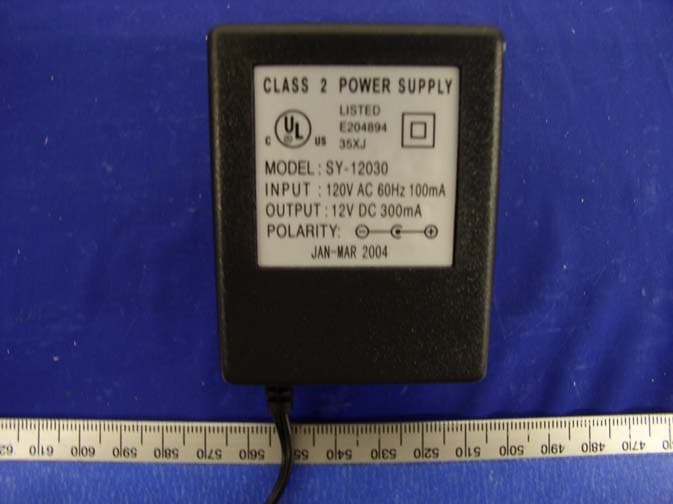
Click to zoom
Application Details
- Equipment Class
- DXX - Part 15 Low Power Communication Device Transmitter
- Date of Grant
- May 05, 2004
- Application Purpose
- Original Equipment
- Date of Application
- May 05, 2004
- Equipment Note
- Wireless A/V Color Carera (2.4G)
- Frequency Range
- 2414.00000000 - 2468.00000000
- Country
- China
Documents & Files
Document Text
Text extracted from the exhibit documents filed with the FCC. Open a document above to read the original.
Users Manual
ZT-813T Wireless Camera MODEL: ZT-813T PAGE: 1 OF 4 PRODUCT INSTRUCTION DESCRIPTION Wireless Camera ZT-813T WIRELESS CAMERA USER’S MANUAL REVISIONS DESCRIPTION DATE DESIGN SHENZHEN ZHONGWANG ELECTRON CO., LTD APPROVAL - 2 - PA G E S TOTAL FILE NUMBER ISSUE DATE CHECK 4 DESIGN FILE NUMBER: MODEL:ZT-813T PAGES: 2 OF 4 Operation instruction 1. Connecting the receiver antenna. (Figure 1) 2. Connecting the 9V/12V direct current stabilizer (Figure 2), pilot lamp lighting (Figure 3). 3. Connecting the audio and video (figure 4) output with the input to the monitor, the television should be set on A/V model. 4. Connecting the audio and video output with the input of the transmitter. 5. Plug power jack of DC power supply(8V , 300mA)into the power socket of the CMOS camera(figure 6).(Battery of the same voltage is acceptable.) 6. Turning the micro-adjustment knob (figure 5) on the receiver till receiving the picture of the wireless camera. 7. Fine tune to the desire position till the image of CMOS camera is received. 8. Adjust the lens of the CMOS camera (figure 7) to best position. Notice 1. The machine is supplied with many different types, please provide with electric power according the value on the label. 2. Obstructs by the building and so on will cause attenuation. 3. Normally that the machine will slightly warm up during operation. 4. Should any other malfunctions occur, please contact local distributor. 5. Under normal operational conditions, one year’s warranty is granted .if there are quality problems within 3 months, this company will unconditionally replace with a new camera. Waning This product is for the sole purpose of security and applicable for monitoring in residential houses, shops and companies. The user shall observe local rules, regulations and laws, and shall be solely liable in this regard. This company shall not be liable for any illegalities therein. Caution: Any changes or modifications not expressly approved by the party responsible for compliance could void the user's authority to operate the equipment. Note: Note: This equipment has been tested and found to comply with the limits for a Class B digital device, pursuant to part 15 of the FCC Rules. These limits are designed to provide reasonable protection against harmful - 3 - interference in a residential installation. This equipment generates, uses and can radiate radio frequency energy and, if not installed and used in accordance with the instructions, may cause harmful interference to radio communications. However, there is no guarantee that interference will not occur in a particular installation. If this equipment does cause harmful interference to radio or television reception, which can be determined by turning the equipment off and on, the user is encouraged to try to correct the interference by one or more of the following measures: --Reorient or relocate the receiving antenna. --Increase the separation between the equipment and receiver. --Connect the equipment into an outlet on a circuit different from that to which the receiver is connected. --Consult the dealer or an experienced radio/TV technician for help. SHENZHEN ZHONGWANG ELECTRON CO., LTD TEL:+86-755-8336 1499 FAX : +86-755-8336 1433 http://www.ztv.cc FILE NUMBER: MODEL:ZT-813T PAGES: 3 OF 4 - 4 - Technical Data ITEM TYPE Transmission Frequency 2.414~2.468GHz 4cH Electric power: DC 12 Video input: 1.0V P-P (MAX) Power consumption current 80mA Audio input: 2V P-P (Max.) Effective range(no obstacles) 30m CMOS IMAGE SENSOR 1/3-inch CMOS Image Sensor CMOS TOTAL PIXELS 628*582 SYNC SYSTEM INTEMAL MINIMUM ILLUMINATION 1 Lμx F1.2 5600°K RESOLUTION 330TV Line Mode: AWB (Zero color rolling) WHITE BALANCE Range:3200~10000°K GAIN CONTROL AGC S/N RATIO 48dB(Min)/60dB(TYP)(AGC OFF) ELECTRONIC SHUTTER 1/60~1/2000ec CAMMA CORRECTION 0.45 OPERATION TEMPERATURE -20°C~60°C OPERATION HUMIDITY 85%RH SHENZHEN ZHONGWANG ELECTRON CO.,LTD TEL:+86-755-8336 1499 FAX : +86-755-8336 1433 http://www.ztv.cc FILE NUMBER: MODEL:ZT-813T PAGES: 4 OF 4 - 5 - . SHENZHEN ZHONGWANG ELECTRON CO.,LTD TEL:+86-755-8336 1499 FAX:+86-755-8336 1433 http://www.ztv.cc : Receiver Antenna : Receiver Power Socket : Receiver Indicator : Audio & Video Jack : Monitor : Camera Power Jack : Flip-type Channel Controller ⑧ : Adjustable Lens
External Photos
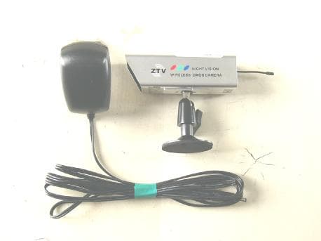
EXHIBIT C - EUT EXTERNAL PHOTOGRAPHS EUT – Chassis Top View EUT – Chassis Side View Adapter View
ID Label/Location Info
EXHIBIT A - FCC ID LABEL INFORMATION Proposed FCC ID Label Specifications : Text is black or white in color and is left justified. Labels are silk- screened and shall be “permanently affixed” at a conspicuous location on the EUT. Proposed Label Location on EUT Side View of EUT / FCC ID Label FCC IDL: Q74ZT-813T This device complies with Part 15 o the FCC Rules. Operation is subject to the following two conditions: (1) this device may not cause harmful interference, and (2) this device must accept any interference received, including interference that may cause undesired operation. 2.1875" 1.0" FCC IDL: Q74ZT812 This device complies wi th Part 15 o the FCC Rules. Operat ion is subject to t he fol low ing two conditions: (1) this device may not cause harmful interference, and (2) this device must accept any interference received, including i nterference that may cause undesired operation. 2.1875" 1. 0 "
Internal Photos
EXHIBIT C - EUT INTERNAL PHOTOGRAPHS EUT – Cover off View EUT – Component View EUT – Solder View I EUT – Solder View II EUT – Antenna Top View EUT – Antenna Bottom View
Operational Description
ZT-813T Wireless Camera Circuit Description The transmitter is made up of two parts: Audio &Video unit and RF unit. The audio signal from MIC1 is amplified, then modulated by the audio carry frequency oscillator (6.5MHz), the modulated carry frequency is added in the VT of voltage controlled oscillator VCO2 (2.4GHz, D1, Q1). The video signal from CMOS camera passes through the sharp network(R4, R5, C11,R16), also is added in the VT of VCO2, another signal is added in the VT of VCO2 is the error voltage output of loop filter (R1,R24,R25,R28,C17,C19,C25) of PLL(U2) which is programmed by CPU(U1), the channel data is decided by the encode switch(SW1) of CPU’s peripheries. The feed back signal (R30,C28) from voltage controlled oscillator VCO2 is compared with reference crystal oscillator, the error frequency of oscillator VCO2 can be corrected. The carry frequency modulated of audio & video has been power amplified by Q2, filtered when through the band pass filter (C20, C18, C23, microstrip) to make the higher harmonica of signal reduce to lower level. The purer signal is emitted by antenna (RFOUT).
Parts List/Tune Up Info
ZT-813T Wireless Camera Bill of Materials (BOM) 1 CMOS.BOM Bill Of Materials for CMOS.sch on Wed Feb 4 15:50:12 2004 Item Qty Reference Part Name Value Description 1 4 Q1-4 2N2222 2 1 MIC MIC6 3 1 U1 OV7910 4 3 C1, C9, C10 ECAP 10uF 5 13 C4-8, C11-C13 CAP0603 0.1uF Y5U CHIP CAPACITOR 6 3 C1, C9, C10 E_04 10uF 7 10 R1, R3, R5, R14 R8-R10, R18, R15, R25 RES0603 10 K 8 1 R16 RES0603 1M 9 1 R17 RES0603 4.7K 10 1 IC1 78L05 11 1 IC2 78L08 12 1 R21 RES0603 0 Ω 13 2 R22, R23 RES0603 10Ω 14 1 R26 RES0603 36K 15 1 R27 RES0603 47K 16 1 R28 RES0603 270 Ω 17 1 R29 RES0603 680 Ω 18 1 R30 RES0603 3.3K 19 2 R31, R32 RES0603 75 Ω 20 1 R33 RES0603 270 Ω 21 2 R19, R37 RES0603 100K 22 1 VR1 VRES 1K 23 1 X1 XTAL1 24 1 CMOS.PCB 32V10 2 RF.BOM Bill Of Materials for RF.sch on Wed Feb 4 16:30:43 2004 Item Qty Reference Part Name Value Description 1 1 D1 HUV316,N N 2 1 Q1 BFG520/XR N48 NPN 3 1 Q2 BFG540/XR N43 NPN 4 1 Q3 2N2222,3904 3904 NPN SWITCH TRANSISTOR 5 1 U1 EM78P153S 6 1 U2 MB15E07SL 7 1 C29 CAP0603,101 101 X7R CHIP CAPACITOR - 2 - 8 5 C1 C12 C16-17 CAP0603,104 104 X7R CHIP CAPACITOR C19 CAP0603,104 104 X7R CHIP CAPACITOR 9 2 C24 C28 CAP0603,1R5 1R5 X7R CHIP CAPACITOR 10 2 C2 C5 CAP0603,33P 33P X7R CHIP CAPACITOR 11 1 C9 CAP0603,102 102 X7R CHIP CAPACITOR 12 3 C7-8 C11 CAP0603,105 105 X7R CHIP CAPACITOR 13 4 C18 C23 C30 C32 CAP0603,2R0 2R0 X7R CHIP CAPACITOR 14 1 C10 CAP0603,10P 10P X7R CHIP CAPACITOR 15 3 C3 C14 C31 CAP0603,121 121 X7R CHIP CAPACITOR 16 1 C6 CAP0603,470 470 X7R CHIP CAPACITOR 17 1 C4 CAP0603,271 271 X7R CHIP CAPACITOR 18 1 C20 CAP0603,3R0 3R0 X7R CHIP CAPACITOR 19 1 C25 CAP0805,475 475 X7R CHIP CAPACITOR 20 2 R4 R29 RES0603,101 101 21 3 R7 R15-16 RES0603,102 102 22 2 R24-25 RES0603,103 103 23 1 R28 RES0603,104 104 24 1 R5 RES0603,180 180 25 1 R10 RES0603,222 222 26 1 R1 RES0603,274 274 27 3 R2 R23 R30 RES0603,301 301 28 2 R11 R22 RES0603,330 330 29 1 R18 RES0603,332 332 30 1 R13 RES0603,333 333 31 2 R3 R17 RES0603,472 472 32 2 R31-32 RES0603,752 752 33 1 L1 IND2520,150 150 34 1 J1 SOP4 SPO4 CONNECTION 35 1 SW1 SW_2BITS 36 1 VC1 VCAP,300 300 37 1 XT2/Y1 XTAL\C 17.7344M 38 1 PCB TA24A3XA RF PCB
Schematics
ZT-813T Wireless Camera Schematic Diagram(SCH) 4.1 CMOS.SCH - 2 - 4.2 IR.SCH - 3 - 4.3 RF.SCH - 4 -
Test Report
Note: This test report is specially limited to the above client company and the product model only. It may not be duplicated without prior written consent of Bay Area Compliance Laboratory Corporation. This report must not be used by the client to claim product endorsement by NVLAP or any agency of the U.S. Government. FCC PART 15 Subpart C EMI MEASUREMENT AND TEST REPORT For SHENZHEN ZHONGWANG ELECTRONICS CO., LTD. 511#, Electrical Equipment Building, No. 72, ZhenHua Road Futian, ShenZhen, P.R.C FCC ID: Q74ZT-813T 2004-05-04 This Report Concerns: Original Report Equipment Type: 2.4GHz Wireless A/V Color Camera, Transmitter Test Engineer: Jerry Wang / Report No.: R0404143(T) Test Date: 2004-04-29 Reviewed By: Ling Zhang / Prepared By: Bay Area Compliance Laboratory Corporation 230 Commercial Street Sunnyvale, CA 94085 Tel (408) 732-9162 Fax (408) 732-9164 SHENZHEN ZHONGWANG ELECTRONICS CO., LTD. FCC ID: Q74ZT-813T Report # R0404143(T)Rpt.doc Page 2 of 19 FCC Part 15.249 Test Report TABLE OF CONTENTS GENERAL INFORMATION.......................................................................................................................................3 PRODUCT DESCRIPTION FOR EQUIPMENT UNDER TEST (EUT) ....................................................................................3 OBJECTIVE...................................................................................................................................................................3 RELATED SUBMITTAL(S)/GRANT(S).............................................................................................................................3 TEST METHODOLOGY..................................................................................................................................................3 TEST FACILITY.............................................................................................................................................................3 SYSTEM TEST CONFIGURATION ..........................................................................................................................5 DESCRIPTION OF TEST CONFIGURATION......................................................................................................................5 EQUIPMENT MODIFICATIONS.......................................................................................................................................5 CONFIGURATION OF TEST SYSTEM..............................................................................................................................5 TEST SETUP BLOCK DIAGRAM.....................................................................................................................................5 POWER SUPPLY INFORMATION.....................................................................................................................................6 SUMMARY OF TEST RESULTS ...............................................................................................................................7 §15.203 - ANTENNA REQUIREMENT......................................................................................................................8 STANDARD APPLICABLE..............................................................................................................................................8 ANTENNA CONNECTED CONSTRUCTION......................................................................................................................8 § 15.249 (C) - CONDUCTED EMISSIONS TEST DATA .........................................................................................9 MEASUREMENT UNCERTAINTY....................................................................................................................................9 EUT SETUP..................................................................................................................................................................9 SPECTRUM ANALYZER SETUP......................................................................................................................................9 TEST EQUIPMENT LIST AND DETAILS...........................................................................................................................9 TEST PROCEDURE........................................................................................................................................................9 ENVIRONMENTAL CONDITIONS..................................................................................................................................10 SUMMARY OF TEST RESULTS.....................................................................................................................................10 CONDUCTED EMISSIONS TEST DATA.........................................................................................................................10 PLOT OF CONDUCTED EMISSIONS TEST DATA...........................................................................................................10 §15.209(A) - RADIATED EMISSION DATA ...........................................................................................................13 MEASUREMENT UNCERTAINTY..................................................................................................................................13 EUT SETUP................................................................................................................................................................13 SPECTRUM ANALYZER SETUP....................................................................................................................................13 TEST EQUIPMENT LIST AND DETAILS.........................................................................................................................14 ENVIRONMENTAL CONDITIONS..................................................................................................…
Text truncated - open the document above for the full version.
Test Setup Photos
EXHIBIT B - TEST SETUP PHOTOGRAPHS Conducted Emission Radiated Emission
Contact Information
Applicant
Tong Ying(R & D Manager)
Test Firm
Bay Area Compliance LaboratoryJohn Chan
Technical Specifications
| # | Rule Parts | Frequency Range | Power Output |
|---|---|---|---|
| 1 | 15C | 2.41 GHz - 2.47 GHz | - |
Other Applications from Shenzhen ZhongWang Electronic Co., Ltd.
Q74ZT-842T
Jun 20, 20052.4GHz Wireless Camera
Equipment Class
DXX - Part 15 Low Power Communication Device Transmitter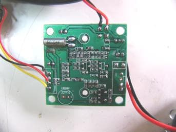
Q74ZT-823T
Jan 19, 20052.4GHz Wireless Camera
Equipment Class
DXX - Part 15 Low Power Communication Device Transmitter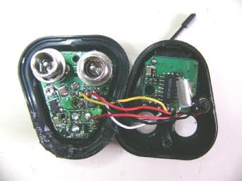
Q74401D
Jan 12, 2005Wireless Converter
Equipment Class
DXX - Part 15 Low Power Communication Device Transmitter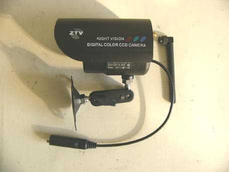
Q74ZT-906T
Dec 13, 20042.4GHz Wireless Camera
Equipment Class
DXX - Part 15 Low Power Communication Device Transmitter
Q74ZT-830T
Nov 07, 20042.4GHz Wireless Camera
Equipment Class
DXX - Part 15 Low Power Communication Device Transmitter