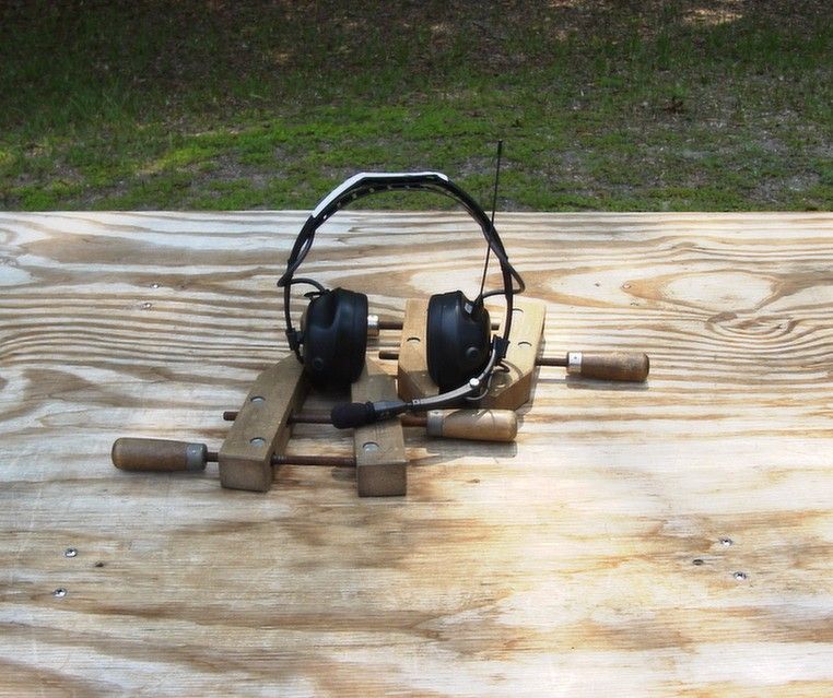
QF9LOCALFamily Radio Transceiver
Hellberg Safety AB
Click to zoom
Application Details
- Equipment Class
- FRE - Part 95 Family Radio Ear Held Transmitter
- Date of Grant
- Mar 17, 2003
- Application Purpose
- Original Equipment
- Date of Application
- Mar 17, 2003
- Equipment Note
- Family Radio Transceiver
- Frequency Range
- 462.56250000 - 467.71250000
- Company
- Hellberg Safety AB
- Country
- Sweden
Documents & Files
Document Text
Text extracted from the exhibit documents filed with the FCC. Open a document above to read the original.
Users Manual
Short pressLong press Channel 1–14 VOX 1–3 Quickstep selection Quickstep selection Change of menu Present menu Instructions for Local 462 Freq. Hz1252505001 k2 k3,15k4k6,38kHML NRR CSA Mean value16,7 19,0 30,8 36,9 36,6 37,4 39,5 43,3 43,6 1 std. deviation2,42,02,22,13,02,42,62,82,536 28 2025A •Frequency: 462 MHz •Channel separation: 25 kHz •Rechargeable NiMH batteries 1600 mAh, rechargeable about 1000 times •Charging time 10 hours •Operates ca. 40 hours after recharging, TX 5% •Delivered with Battery Charger •Automatic shut off after 4 hours • Transmitting power .145W ERP •VOX – 3 Levels of sensitivity to suit the surrounding noise level •Number of channels: 14 •EPS – Electronic Protection System which allows for max. 82 dB(A) inside the earcups •CEPS – Communication Electronic Protection System - Incoming signals are being transmitted up to 82 dB(A) only •Simple Easy-Step function for selecting mode quickly within each menue •Synth. Voice guides through the menues stating menue and mode chosen •Volume control – separate for Level Dependant and for communication Technical Specifications Tested at ANSI S3.19-1974, weight 12.2 oz. Accessories How to use and take care of my hearing protector All hearing protectors, which are included in this instruction sheet, are equipped with a headband or spring arms of thermoplastic and foam plastic filled cushions. Use To attain highest comfort and protection from this hearing protector you shall: - use, take care of and adjust the protector in accordance with the instructions below. - regularly check that no parts are worn- out and that there are no cracks in the protector. Adjust (Headband) Adjust the protector to its largest size and put it on. See to it that your ears are totally encompassed by the cups and that you get an even pressure around your ears. Now adjust the cups so that the headband rests lightly on your head. Adjust (Helmet mounted) Adjust the earmuff to the largest size, then fit the earcups over your ears so that they sit comfortably and snugly. Now re-adjust the helmet so that it sits lightly on your head. Warning If the above instructions are not observed the attenuation effect can dramatically decrease. Care The hearing protector and the cushions will be worn and must be checked regularly. Clean with mild detergent (soap). You must be sure that the deter- gent does not irritate your skin. The hea- ring protector is to be kept in a dry and clean place, for example in the original packing. Maintenance Remove the self-adhesive cushion. Rem- ove the protective film from the cushion and place the cushion around the hole and press. Choose the right hygiene kit for your hearing protector. Read the instructions carefully before use. Remote PTT-button As an accessory there is an extra PTT- button with a clamp connection. Art. No. 99520 Hellberg Fresh Self-adhesive hygiene ring which is heat absorbing and makes the hearing protector more comfortable and hygienic. Art. No. 99900 Hygiene kit New cushions and outer absorbent, which should be exchanged at least once every six months. Art. No. 99042. Wind shield (cup-mic) Art. No. 99510 Wind shield (boom mic) Art. No. 99515 Local 462 User instructions On/Off and Volume Starts electronics, controls volume of Active listening function and of the integrated communication radio PTT – button Press and hold down when transmitting Aux socket Connect charger and charge for 10 hours. This intake is also for connecting an external PTT – button, Walkman, CD- Player, Comm.-Radio etc. Mode Button For changing menues and to select VOX/PTT transmittance or channels On/Off Volume Active listening Com-radio UNITED STATES FCC ID: QF9LOCAL This device complies with Part 15 of the FCC Rules. Operation is subject to the following conditions (1) This device may not cause harmful interference, and (2) this device must accept any interference received, including interference that may cause undesired operation. Safety information Y our wireless transceiver contains low power transmitter. When the transmitter is activated it sends out radio frequency (RF) signals. This device is authorized to operate at a duty factor not exceed 50%.Use only the supplied antenna. Unauthorized antennas, modifications, or attachments could damage the transmitter and violate FCC regulations
Block Diagram
SECTION 10 BLOCK DIAGRAM 10 - 1 DS1LN1371G CTCIN D/A REMINPTT2MICSWMMUTRMUTAFONRXVTXVPOWER LCD DS2: LD-BU10503J VOLTSENS RESET IC5: S-80928ANMP X2CDBCA450CX24 FI3:CFWM450G CERAMICBPF FMDET S OUT IFAMP NOISEDET IC2TA31136FN Q13: 2SC4081Q14: 2SA1586D8 : 1SS355D9 : 1SS355 Q6: 2SC5108D4, D5: 1SV284 X1CR-669(21.25 MHz) 2nd.Lo: 21.25 MHz 2nd MIX IC1μ PD3140GS UNLOCKDATA/UNLK, CK, STB Q1: 2SC4215 FI2: FL-297 Q72SC5108 R50MOD LEVEL SET VCO BUFF LOSW D1: MA77D2: MA77 PWRAMP DRIVEAMP PREDRIVE D7: MA2S077D101: MA2S077D102: MA2S077 POWER SETR206 IC3: AT24C02N EEPROM X1CR-627(5.8368 MHz) POWERMODEUPDOWNPTTS1 CPUIC1μ PD753036GK AFVOLTXMOD Q72SC4081 TONELPFTONELPF Q122SC4081 MODSW Q1DTA144EU LPF IDC +3V IC2ANJM2100M Q62SK1829 MICMUTE IC2BNJM2100M Q232SJ144 R58AF VOL VOLMUTE MC1KUC3523 PTTSENSE MICSW MIC R+3CURRENTAMP R+3 T+3 +3VCURRENTAMP Q25: UMZ2ND4: 1SS355 +3V to LOGIC +3REG IC6S-81230SG Q182SA1586 Q27 : 2SC4081Q28 : 2SB798Q101: UMZ1ND5: 1SS355 T+3CURRENTAMP D2: 1SS355 PROTECTOR Q29: DTC114EU Q2: UN9214Q3: DTA123JUA AFMUTE BATT BATTERY J3 COMON LINETX LINERX LINEDATA BUS LINE J1 SP1 AFAMP IC9NJM2070M Q5 : 2SA1362Q10: 2SC4081Q11: 2SC4213 Q23SK284 Q3: 2SC5194 RFAMP ANTSW HPF LPF ANT CHASSIS UNT Q15: 2SC4081Q16: 2SC4081 VCOREG PLLIC AF FIL 1st IF: 21.7 MHz 1st.LORX Frequency 21.700 MHz TX/RX: Frequency 446.00625 – 446.09375 MHz 1st MIX FI1: NSVS647 SHIFT Q122SC5006 Q202: XRF9482 Q201: 2SC3356 D103: MA2S728 Q8: 2SC4228 SQL SENS PSC LOOPFIL IFAMP XTALBPF BPF CHASSIS UNIT RF UNITMAIN UNIT Q2032SC5108 BUFF RX-LOSHUNT SW R+3 Q14DTA114EU LEDDRV SP JACKMIC JACK
ID Label/Location Info
LeftRight FCC ID Label Local Product sign Serial No. 02-10-12345 Serial No. FCC id. Product sign FCC ID: QF9LOCAL
Operational Description
4 - 1 SECTION 4CIRCUIT DESCRIPTION 4-1 RECEIVER CIRCUITS 4-1-1 ANTENNA SWITCHING CIRCUIT (RF UNIT) Received signals from the antenna connector are passed through the low-pass filter (L5, L6, C8–C12). The filtered sig- nals are applied to the λ ⁄4type antenna switching circuit (D101, D102, L4, L206, C209, C210). The passed signals are then applied to the RF amplifier circuit. The antenna switching circuit functions as a low-pass filter while receiving. However, its impedance becomes very high while D101 and D102 are turned ON (while transmitting). Thus transmit signals are blocked from entering the receiv- er circuits. The passed signals are then applied to the RF amplifier circuit. 4-1-2 RF CIRCUIT (RF UNIT) The RF circuit amplifies signals within the range of frequen- cy coverage and filters out-of-band signals. The signals from the antenna switching circuit are amplified at the RF amplifier (Q3) and passed through the bandpass filter (FI1) to suppress out-of-band signals. The filtered sig- nals are applied to the 1st mixer circuit. 4-1-3 1ST MIXER AND 1ST IF CIRCUITS (RF UNIT) The 1st mixer circuit converts the received signals to a fixed frequency of the 1st IF signal with a PLL output frequency. By changing the PLL frequency, only desired signals will pass through a crystal filter at the next stage of the 1st mixer. The signals from the bandpass filter (FI1) are mixed at the 1st mixer circuit (Q2) with a 1st LO signal coming from the VCO circuit to produce a 21.7 MHz 1st IF signal. The 1st IF signal is applied to a crystal filter (FI2) to sup- press out-of-band signals. The filtered 1st IF signal is applied to the IF amplifier (Q1), then applied to the 2nd mixer circuit. 4-1-4 2ND MIXER AND DEMODULATOR CIRCUITS (RF UNIT) The 2nd mixer circuit converts the 1st IF signal into a 2nd IF signal. A double conversion superheterodyne system (which converts receive signals twice) improves the image rejection ratio and obtains stable receiver gain. The 1st IF signal from the IF amplifier (Q1) is applied to the 2nd mixer section in the FM IF IC (IC2, pin 16), and is mixed with the 2nd LO signal to be converted into a 450 kHz 2nd IF signal. The FM IF IC contains a 2nd mixer, quadrature detector, noise amplifier and a limiter amplifier, etc. The PLL refer- ence oscillator (X1) is used for the 2nd LO signal via the PLL IC (IC1, pins 16, 17), and is applied to pin 1 of the FM IF IC (IC2). The mixed 2nd IF signal is output from pin 3 (IC2) and passed through the ceramic bandpass filter (FI3) to remove unwanted heterodyne frequencies. It is then amplified at the limiter amplifier section (IC2, pin 5) and applied to the quad- rature detector section (IC2, pins 10, 11) to demodulate the 2nd IF signal into AF signals. 4-1-5 AF CIRCUIT (RF AND MAIN UNITS) AF signals from the FM IF IC (RF unit; IC2, pin 9) are passed through the high-pass filter (RF unit; Q15, Q16) to remove CTCSS signals then applied to the MAIN unit via J2 (pin 10) as the “VOL” signal. The “VOL” signal (AF signals) from the RF unit is applied to the [VOL] control (MAIN unit; R58) to control the audio level via the volume mute switch (Q23). The level controlled AF signals are applied to the AF power amplifier (IC9, pin 2) to drive an internal speaker (SP1) via the [SP] jack (J1). • 2nd IF and demodulator circuits Mixer 16 Limiter amp. 2nd IF filter 450 kHz PLL IC IC1 X1 21.25 MHz X2 (21.25 MHz) RSSI IC2 TA31136FN 14 1st IF (21.7 MHz) from Q1 "SQL" signal to the CPU pin 59 11109 87 53 AF signal "AF" R+3 1 17 16 Active filter FI3 Noise detector FM detector 4 - 2 4-1-6 SQUELCH CIRCUIT (RF AND MAIN UNITS) • NOISE SQUELCH The noise squelch circuit cuts out AF signals when no RF signals are received. By detecting noise components in the AF signals, the squelch circuit switches the AF mute switch. A portion of the AF signals from the FM IF IC (RF unit; IC2, pin 9) are applied to the active filter section (RF unit; IC2, pin 8). The active filter section amplifies and filters noise components. The filtered signals are applied to the noise detector section and output from pin 14 as the “SQL” signal. The “SQL” signal from IC2 (pin14) is applied to the CPU (MAIN unit; IC1, pin 59). The CPU analyzes the noise con- dition and outputs the “RMUT” and “AFON” signals to toggle the volume mute (MAIN unit; Q23) and AF mute (MAIN unit; Q5, Q10, Q11) switches. • TONE SQUELCH The tone squelch circuit detects AF signals and opens the squelch only when receiving signal containing a matching subaudible tone (CTCSS). When tone squelch is in use, and a signal with a mismatched or no subaudible tone is received, the tone squelch circuit mutes the AF signals even when noise squelch is open. A portion of the AF signals from the FM IF IC (RF unit; IC2, pin 9) passes through the tone low-pass filter (MAIN unit; Q7, Q12) to remove AF (voice) signals and is applied to the CTCSS decoder inside the CPU (MAIN unit; IC1, pin 58) via the “CTCIN” line to control the volume mute and AF mute switches. 4-2 TRANSMITTER CIRCUITS 4-2-1 MICROPHONE AMPLIFIER CIRCUIT (MAIN UNIT) The microphone amplifier circuit amplifies audio signals with pre-emphasis characteristics from the microphone to a level needed for the modulation circuit. AF signals from the internal/external microphone are applied to the microphone amplifier circuit (IC2b) via the microphone mute switch (Q6) and pre-emphasis circuit (R7, C24). The amplified signals are passed through the splatter filter (IC2a) and applied to the modulation circuit in the RF unit via J4 (pin 6) as the MOD signal. 4-2-2 MODULATION CIRCUIT (RF UNIT) The modulation circuit modulates the VCO oscillating signal (RF signal) using the microphone AF signals. The filtered audio signals from the MAIN unit are passed through the deviation adjustment pot (R50), and are then applied to the modulation circuit (D4, D5) to modulate trans- mit signals at the VCO circuit (Q6). The modulated signal is applied to the drive amplifier circuit. 4-2-3 DRIVE/POWER AM…
Text truncated - open the document above for the full version.
Parts List/Tune Up Info
5 - 2 SECTION 5 ADJUSTMENT PROCEDURES 5-1 PREPARATION nREQUIRED TEST EQUIPMENT EQUIPMENT DC power supply Frequency counter FM deviation meter DC voltmeter RF power meter (terminated type) GRADE AND RANGE Output voltage: 4.5 V DC Current capacity: 1 A or more Frequency range: 0.1–600 MHz Frequency accuracy : ±1 ppm or better Sensitivity: 100 mV or better Frequency range: 30–600 MHz Measuring range: 0 to ±10 kHz Input impedance: 50 kΩ/V DC or better Measuring range: 100 mW–1 W Frequency range: 300–600 MHz Impedance: 50 Ω SWR: Less than 1.2 : 1 EQUIPMENT Audio generator Standard signal generator (SSG) Oscilloscope AC millivoltmeter External speaker Attenuator GRADE AND RANGE Frequency range: 300–3000 Hz Measuring range: 1–500 mV Frequency range: 0.1–600 MHz Output level: 0.1 μV–32 mV (–127 to –17 dBm) Frequency range: DC–20 MHz Measuring range: 0.01–10 V Measuring range: 10 mV–10 V Input impedance: 8 Ω Capacity: 300 mW or more Power attenuation: 30 or 40 dB Capacity: 1 W or more nENTERING THE ADJUSTMENT MODE qTurn the transceiver power OFF. wWhile connecting the “TEST” and GND on the MAIN unit, then turn power ON. (See location at page 5-3) nCONNECTIONS to the RF test port J1 Standard signal generator –17 to –127 dBm (32 mV to 0.1 μV) CAUTION: DO NOT transmit while SSG is connected to the antenna connector. Frequency counter FM deviation meter Attenuator 30 dB or 40 dB RF power meter 50 Ω/100 mW–1 W DC power supply 4.5 V/1.0 A – + 5 - 3 REFERENCE FREQUENCY OUTPUT POWER FM DEVIATION 5-2 PLL AND TRANSMITTER ADJUSTMENTS ADJUSTMENT ADJUSTMENTADJUSTMENT CONDITION MEASUREMENT VALUE POINT UNITLOCATIONUNIT ADJUST 466.00625 MHz .145W erp ±2.45 kHz 10 mV ±3dB 1 1 1 2 • Operating channel : Ch 01 • Transmitting • Operating channel : Ch 01 • Transmitting • Operating channel : Ch 01 • Set group No.: 01 • Connect an audio generator to the [MIC] jack and set as: 1 kHz/100 mV rms • Set an FM deviation meter as: HPF: OFF LPF: 20 kHz or 15 kHz De-emphasis : OFF Detector: (P–P)/2 • Transmitting • Set group No.: OFF (– –) • Set an audio generator output level until the deviation is ±1.75 kHz. • Transmitting To p panel RF RF Loosely couple a fre- quency counter to the antenna. Connect an RF power meter to the RF test port J1. Connect an FM devia- tion meter to the RF test port J1. RF RF RF C63 R206 R50 Verify RF GND J1 RF test port R50 FM deviation adjustment Reference frequency adjustment R206 Output power adjustment TEST C63 5 - 4 SQUELCH 5-3 RECEIVER ADJUSTMENT ADJUSTMENTADJUSTMENT CONDITION MEASUREMENT VALUEADJUSTMENT UNITLOCATION Audio signal disappears. 1 2 • Operating channel : Ch 04 • Connect an SSG to J1 on the RF unit and set as: Frequency: 446.04375 MHz Level: 0.14 μV* (–124 dBm) Modulation: OFF • Receiving • Set an SSG as: Level: OFF • Receiving Front panel Internal speaker Push and hold [MODE] and [DOWN] keys for 1 sec. Verify
Parts List/Tune Up Info
[MAIN UNIT][MAIN UNIT] IC11140008770 S.ICμPD753036GK-559-BE9 IC21110002820 S.ICNJM2100M-T1 IC31140008350 S.ICAT24C02N-10SI-2.7 IC51110004710 S.ICS-80928ANMP-DDR-T2 IC61180001150 S.ICS-81230SG-QB-T1 IC91110002810 S.ICNJM2070M-T1 Q11590000720 S.TRANSISTORDTA144EUA T106 Q21590001440 S.TRANSISTORUN9214 (TX) Q31590002920 S.TRANSISTORDTA123JUA T106 Q51510000580 S.TRANSISTOR2SA1362-GR (TE85R) Q61560000840 S.FET2SK1829 (TE85R) Q71530002280 S.TRANSISTOR2SC4081 T107 S Q101530002280 S.TRANSISTOR2SC4081 T107 S Q111530003090 S.TRANSISTOR2SC4213-B (TE85R) Q121530002280 S.TRANSISTOR2SC4081 T107 S Q141590001330 S.TRANSISTORDTA114EUA T106 Q181510000770 S.TRANSISTOR2SA1586-GR (TE85R) Q231590001390 S.FET2SJ144-Y (TE85R) Q251590002490 S.TRANSISTORUMZ2N TR Q271530002280 S.TRANSISTOR2SC4081 T107 S Q281520000200 S.TRANSISTOR2SB798-T2 DK Q291590000680 S.TRANSISTORDTC114EUA T106 Q1011590002630 S.TRANSISTORUMZ1N TR D21750000550 S.DIODE1SS355 TE-17 D41750000550 S.DIODE1SS355 TE-17 D51750000550 S.DIODE1SS355 TE-17 X16050010450 S.XTALCR-627 (5.8368 MHz) R27030003670 S.RESISTORERJ3GEYJ 823 V (82 kΩ) R47030003670 S.RESISTORERJ3GEYJ 823 V (82 kΩ) R57030003810 S.RESISTORERJ3GEYJ 125 V (1.2 MΩ) R67030003710 S.RESISTORERJ3GEYJ 184 V (180 kΩ) R77030003450 S.RESISTORERJ3GEYJ 122 V (1.2 kΩ) R97030003680 S.RESISTORERJ3GEYJ 104 V (100 kΩ) R107030003310 S.RESISTORERJ3GEYJ 820 V (82 Ω) R127030003200 S.RESISTORERJ3GEYJ 100 V (10 Ω) R137030003520 S.RESISTORERJ3GEYJ 472 V (4.7 kΩ) R147030003500 S.RESISTORERJ3GEYJ 332 V (3.3 kΩ) R227030003620 S.RESISTORERJ3GEYJ 333 V (33 kΩ) R237030003580 S.RESISTORERJ3GEYJ 153 V (15 kΩ) R247030003820 S.RESISTORERJ3GEYJ 155 V (1.5 MΩ) R257030003570 S.RESISTORERJ3GEYJ 123 V (12 kΩ) R267030003560 S.RESISTORERJ3GEYJ 103 V (10 kΩ) R277030003320 S.RESISTORERJ3GEYJ 101 V (100 Ω) R307030003580 S.RESISTORERJ3GEYJ 153 V (15 kΩ) R317030003800 S.RESISTORERJ3GEYJ 105 V (1 MΩ) R327030003780 S.RESISTORERJ3GEYJ 684 V (680 kΩ) R337030003540 S.RESISTORERJ3GEYJ 682 V (6.8 kΩ) R347030003540 S.RESISTORERJ3GEYJ 682 V (6.8 kΩ) R357030003530 S.RESISTORERJ3GEYJ 562 V (5.6 kΩ) R367030003560 S.RESISTORERJ3GEYJ 103 V (10 kΩ) R377030003600 S.RESISTORERJ3GEYJ 223 V (22 kΩ) R387030003600 S.RESISTORERJ3GEYJ 223 V (22 kΩ) R397030003670 S.RESISTORERJ3GEYJ 823 V (82 kΩ) R407030003680 S.RESISTORERJ3GEYJ 104 V (100 kΩ) R417030003530 S.RESISTORERJ3GEYJ 562 V (5.6 kΩ) R427030003500 S.RESISTORERJ3GEYJ 332 V (3.3 kΩ) R437030003650 S.RESISTORERJ3GEYJ 563 V (56 kΩ) R457030003840 S.RESISTORERJ3GEYJ 225 V (2.2 MΩ) R467030003320 S.RESISTORERJ3GEYJ 101 V (100 Ω) R497030003320 S.RESISTORERJ3GEYJ 101 V (100 Ω) R507030003520 S.RESISTORERJ3GEYJ 472 V (4.7 kΩ) R517030003760 S.RESISTORERJ3GEYJ 474 V (470 kΩ) R527030003740 S.RESISTORERJ3GEYJ 334 V (330 kΩ) R537030003820 S.RESISTORERJ3GEYJ 155 V (1.5 MΩ) R547030003450 S.RESISTORERJ3GEYJ 122 V (1.2 kΩ) R557030003330 S.RESISTORERJ3GEYJ 121 V (120 Ω) R567030004050 S.RESISTORERJ3GEYJ 1R0 V (1 Ω) R577030003580 S.RESISTORERJ3GEYJ 153 V (15 kΩ) S.=Surface mount R587210001970 VARIABLERV-244 R597030003680 S.RESISTORERJ3GEYJ 104 V (100 kΩ) R617030003280 S.RESISTORERJ3GEYJ 470 V (47 Ω) R627030003680 S.RESISTORERJ3GEYJ 104 V (100 kΩ) R637030003530 S.RESISTORERJ3GEYJ 562 V (5.6 kΩ) R647030003590 S.RESISTORERJ3GEYJ 183 V (18 kΩ) R657030003590 S.RESISTORERJ3GEYJ 183 V (18 kΩ) R667030003590 S.RESISTORERJ3GEYJ 183 V (18 kΩ) R677030003590 S.RESISTORERJ3GEYJ 183 V (18 kΩ) R687030003590 S.RESISTORERJ3GEYJ 183 V (18 kΩ) R697030003590 S.RESISTORERJ3GEYJ 183 V (18 kΩ) R707030003660 S.RESISTORERJ3GEYJ 683 V (68 kΩ) R717030003620 S.RESISTORERJ3GEYJ 333 V (33 kΩ) R727030003800 S.RESISTORERJ3GEYJ 105 V (1 MΩ) R747030003560 S.RESISTORERJ3GEYJ 103 V (10 kΩ) R767030003680 S.RESISTORERJ3GEYJ 104 V (100 kΩ) R777030003400 S.RESISTORERJ3GEYJ 471 V (470 Ω) R787030003560 S.RESISTORERJ3GEYJ 103 V (10 kΩ) R797030003720 S.RESISTORERJ3GEYJ 224 V (220 kΩ) R807030003680 S.RESISTORERJ3GEYJ 104 V (100 kΩ) R817030003560 S.RESISTORERJ3GEYJ 103 V (10 kΩ) R867030003680 S.RESISTORERJ3GEYJ 104 V (100 kΩ) R877030003800 S.RESISTORERJ3GEYJ 105 V (1 MΩ) R887030003680 S.RESISTORERJ3GEYJ 104 V (100 kΩ) R897030003440 S.RESISTORERJ3GEYJ 102 V (1 kΩ) R907030003440 S.RESISTORERJ3GEYJ 102 V (1 kΩ) R947030003720 S.RESISTORERJ3GEYJ 224 V (220 kΩ) R957030003520 S.RESISTORERJ3GEYJ 472 V (4.7 kΩ) R967030003680 S.RESISTORERJ3GEYJ 104 V (100 kΩ) R977030003680 S.RESISTORERJ3GEYJ 104 V (100 kΩ) R987030003680 S.RESISTORERJ3GEYJ 104 V (100 kΩ) R997030003680 S.RESISTORERJ3GEYJ 104 V (100 kΩ) R1007030003680 S.RESISTORERJ3GEYJ 104 V (100 kΩ) R1017030003680 S.RESISTORERJ3GEYJ 104 V (100 kΩ) R1027030003680 S.RESISTORERJ3GEYJ 104 V (100 kΩ) R1037030003680 S.RESISTORERJ3GEYJ 104 V (100 kΩ) R1057030003560 S.RESISTORERJ3GEYJ 103 V (10 kΩ) R1067030003560 S.RESISTORERJ3GEYJ 103 V (10 kΩ) R1087030003620 S.RESISTORERJ3GEYJ 333 V (33 kΩ) R1107030003800 S.RESISTORERJ3GEYJ 105 V (1 MΩ) R1127030003560 S.RESISTORERJ3GEYJ 103 V (10 kΩ) R1147030003500 S.RESISTORERJ3GEYJ 332 V (3.3 kΩ) R1157030003410 S.RESISTORERJ3GEYJ 561 V (560 Ω) R1177030003680 S.RESISTORERJ3GEYJ 104 V (100 kΩ) R1187030003520 S.RESISTORERJ3GEYJ 472 V (4.7 kΩ) R1197030003680 S.RESISTORERJ3GEYJ 104 V (100 kΩ) R2007030003840 S.RESISTORERJ3GEYJ 225 V (2.2 MΩ) R2017030003370 S.RESISTORERJ3GEYJ 271 V (270 Ω) R2027030003320 S.RESISTORERJ3GEYJ 101 V (100 Ω) R2037030003550 S.RESISTORERJ3GEYJ 822 V (8.2 kΩ) R2047030003540 S.RESISTORERJ3GEYJ 682 V (6.8 kΩ) C14030008470 S.CERAMICC1608 JB 1H 272K-T-A C34030011600 S.CERAMICC1608 JB 1C 104KT-N C44030011600 S.CERAMICC1608 JB 1C 104KT-N C54030006850 S.CERAMICC1608 JB 1H 471K-T-A C64030008680 S.CERAMICC2012 JF 1C 105Z-T-A C74030011600 S.CERAMICC1608 JB 1C 104KT-N C84510004630 S.ELECTROLYTIC ECEV1CA100SR C94030006850 S.CERAMICC1608 JB 1H 471K-T-A C104030006850 S.CERAMICC1608 JB 1H 471K-T-A C114030006850 S.CERAMICC1608 JB 1H 471K-T-A C154030011600 S.CERAMICC1608 JB 1C 104KT-N C174550006880 S.TANTALUMTEMSVD2 0J 157M-12R C184510004630 S.ELECTROLYTIC ECEV1CA100SR C204030011600 S.CERAMICC1608 JB 1…
Text truncated - open the document above for the full version.
Schematics
SECTION 11 VOLTAGE DIAGRAM 11 - 1 11-1 MAIN UNIT LON: 0LOF: 3.02 LON: 0.76LOF: 0 C: 3.81 T: 3.05R: 2.37 C: 3.02 C: 3.10 C: 1.44 T: 0R: 0.88 C: 1.95 T: 0R: 2.95 C: 3.12 T: 0R: 3.02 C: 3.10 T: 1.58R: 0 T: 3.05R: 0 T: 1.51R: 0 C: 0 C: 3.12 T: 1.53R: 0 T: 1.50R: 0 C: 2.46 C: 3.11 T,SC: 0SO: 0.69 T: 0SO: 2.93SC: 0 T: 3.91SO: 3.87SC: 3.93 T: 0SO: 2.30SC: 0 T: 0SC: 0SO: 4.63 T: 3.02R: 0 T: 2.64R: 0 T,SC: 0SO: 1.99 T: 0.80R: 0 T: 3.67R: 4.41 T: 0.18R: 0 C: 3.64 T: 2.79SO: 0SC: 2.79 T: 0R: 3.12 T: 3.02R: 0 T: 2.79R: 0 T: 1.60R: 0 C: 3.02 T: 3.64R: 0 R101100 k R102100 k R98100 k R117100 k R59100 k R99100 k R100100 k S1SW-149 W2 PTT DOWN UP MODE POWER C750.001 R6818 k R6918 k C530.1 NC 1 NC 2 NC 3 VSS 4 SDA 5 SCL 6 NC 7 VCC 8 IC3AT24C02N C4524 P X1CR-627 R721 M C4624 P R6147 R2046.8 k Q14DTA114EU DS1LN1371G R96100 k R901 k C92470 P R67 18 k R71 33 k R70 68 k R891 k R97100 k C740.001 REMIN EEPDARXVEEPCKPSCRESETTXVLAMPCMICSWMMUTE AN3 61 P73/KR7 80 AN4 62 AN5 63 AVSS 64 AVREF 65 VDD 66 XT1 67 XT2 68 IC 69 X1 70 X2 71 RESET 72 P60/KR0 73 P61/KR1 74 P62/KR2 75 P63/KR3 76 P70/KR4 77 P71/KR5 78 P72/KR6 79 SQLIN CTCIN TXMOD CTCO2 CTCO1 CTCO0 POWER PLLST PLLDA PLLCK AFON RMUTE BEEP TEST CLIN 60 59 58 57 56 55 54 53 52 51 50 49 48 47 46 45 44 43 42 41 AN2 AN1 AN0 P83/AN7 P82/AN6 P31/SYNC P30/LCDCL P23/BUZ P22/PCL/PTO2 P21/PTO1 P20/PTO0 P13/TI0 P12/TNT2 P11/TNT1 P10/TNT0 P03/SI/SB1 P81/TI2 P80/TI1 P33 P32 COM0 21 P02/SO/SB0 40 COM1 22 COM2 23 COM3 24 BIAS 25 VLC0 26 VLC1 27 VLC2 28 P40 29 P41 30 P42 31 P43 32 VSS 33 P50 34 P51 35 P52 36 P53 37 P00/INT4 38 P01/SCK 39 S31/BP7 S30/BP6 S29/BP5 S28/BP4 S27/BP3 S26/BP2 S25/BP1 S24/BP0 S23 S22 S21 S20 S19 S18 S17 S16 S15 S14 S13 S12 S25 SHIFT S24 S23 S22 S21 S20 S19 S18 S17 S16 S15 S14 S13 S12 1 2 3 4 5 6 7 8 9 10 11 12 13 14 15 16 17 1 2 3 4 5 6 7 8 9 10 11 12 13 14 15 16 17 18 19 20 SEG25 SEG24 SEG23 SEG22 SEG21 SEG20 SEG19 SEG18 SEG17 SEG16 SEG15 SEG14 SEG13 SEG12 COM0 COM1 COM2 COM0 COM1 COM2 DS2LD-BU10503J R6518 k R6618 k R6418 k +3 V SHIFT VOL CKDATASTBAFSENSSQLMOD PSCR+3T+3BATT 12345 6 7 8 9 10 11 12 13 14 J4 8 IC2aNJM2100M R3015 k C730.0033 T-ID 1 32 4 C10.0027 C990.0033 R282 k R2038.2 k R3982 k C29150 P R40100 k Q2UN9214 Q3DTA123JUA Q1DTA144EU C61 PTT2 Q62SK1829 RMUTEAFONBEEP Q182SA1586 GR R8110 k R74 10 k C610.1 BATIN C560.1 R80100 k R94220 k C672.2 R79 220 k R76100 k OUT C600.1 +3 V TXVRXV C630.1 C94330 P D41SS355 W7 R77470 C89470 P 321 6 5 4 Q25UMZ2N C650.1 R7810 k GND 1 VIN 2 VOUT 3 NC NC R541.2 k R55120 C490.1 C4822 Q102SC4081 SQ52SA1362 GR C47470 P C553.3 R2315 k IC9NJM2070M C522.2 R561 C500.1 C17150 Q112SC4213 B R2610 k C1810 C97330 P C96330 P W5 J3 R58RV-24410 k C98330 P SP1CHASSIS C200.1 D21SS355 R2512 k 1 REMIN 2 3 4 5678 R452.2 M C360.001 C400.1 R46100 R355.6 k Q122SC4081 S C510.1 R5715 k R346.8 k C26470 P C270.1 C280.047 R336.8 k R32680 k C320.1 C310.022 C340.0047 R3822 k R3610 k R3722 k R415.6 k Q72SC4081 S C240.033 R531.5 M BEEP R423.3 k R4356 kC350.1 R51.2 M R71.2 k R10833 k R482 k 7 IC2bNJM2100M C850.1 R52330 k R1184.7 k MMUTE C93330 P C30.1 R9100 k R504.7 k C5470 P C790.1 R95 4.7 k MC1 KUC3523 R143.3 k C10470 P C11470 P Q29DTC114EU VOLUME C40.1 C25470 P R1101 M C210.1 C150.1 R22 33 k R27100 Q232SJ144 Y R871 M R86100 k R88100 k C59470 P C720.01 C570.1 R11210 k R2002.2 M C860.1 Q272SC4081 S BATT R1143.3 k D51SS355 R115560 6 5 4 321 Q101UMZ1N Q282SB798 DK R+3 SENINBATIN RXD TEST R103100 k R62100 k PTT2 R10510 k 56 R6180 k R202100 R134.7 k R1082 W3 C810 C90470 P R12 10 R49100 C9470 P C420.01 J1 C95330 P C440.1 C70.1 C91470 P R51470 k C830.1 REMIN VDD VSS NC NC IC5 S-80928ANMP C80100 C620.1 C88470 P C810.033 4 5 12 3 R311 M C540.1 R+3 C6422 R635.6 k IC6 S-81230SG 45 R24 1.5 M C820.047 R10610 k C87470 P C : COMMON T: TXR : RX SO : SQL OPENSC : SQL CLOSELON : LIGHT ONLOF : LIGHT OFF C710.1 R201270 R119100 k IC1μ PD753036GK-559-BE9 to RF unit J2 11-2 RF UNIT 11 - 2 T: 0R: 0.72 T: 0R: 1.83 T: 0R: 2.60 T: 0R: 1.72 T: 0R: 2.94 T: 0R: 0.77 T: 0R: 2.28 T: 0R: 0.27 T: 0R: 2.19 C: 2.82 T: 0R: 0.97 T: 0R: 1.84 T: 0R: 1.85 C: 4.5 C: 3.02 C: 2.99 C: 3.06 C: 0.75 C: 0.70 T: 2.24R: 0 T: 0.85R: 0 T: 2.85R: 0.01 C: 1.89 C: 1.22 T: 0R: 0.75 T: 0.85R: 0 T: 1.67R: 0 T: 1.45R: 0.40T: 0R: 1.14 T: 0.46R: 0.84 T: 2.95R: 0 T: 2.37R: 0 T: 1.78R: 0 T: 3.64R: 0 T: 0R: 2.94 C: 2.47 T: 0R: 0.98 CHASSIS EP1 C730.1 C74470 P C75470 P R51560 k 1 2 3 4 5 FI3CFWM450G R521.5 k R53150 k 2nd-Lo (21.25 MHz) R1820 C10.001 Q12SC4215 O FI2FL-297 C20.047 C7910 R31 k C4722 P R282 k C1011 P EP2 MMZ1608D121B C28470 P R64.7 k C350.001 C30.047 R30347 k R304270 C2120.001 R310330 k L2090.1 μ H R19330 L12.2 μ H C4612 P R4560 C368 P C2195 P C1347 P L21127 nH Q23SK284 R747 C5470 P C6470 P C65470 P R2533 k L412 nH 12 FI1NSVS647 D102MA2S077 L318 nH C326P R1633 Q32SC4226 R25 C722 P R+3 1st LO C86 P C128 P C110.75 P C91.5 P C1010 P L20618 nH L617 nH L517 nH D101MA2S077 C2096P C2107 P C307 P C4427 P L1022 nH D7MA2S077 C317 P RF TEST PORT 12 J1 C72470 P L20568 nH L2315 nH R209220 R+3 C20222 P C2078 P C2089 P L2048.2 nH C2060.001 R2071 k C2050.001 Q202XRF9482 R20510 k R20610 k L20339 nH R3018.2 k C21470 P C26470 P C201470 P Q82SC4228 R44 L20233 nH L20122 nH W202 Q2012SC3356 R24 W201 C20322 P R213220 R8668 L2122 nH C2046 P T+3 C237 P R20222 k D2MA77 C70470 P D1MA77 R121 k R2081 k R3722 k C1022 P C8810 C16470 P R3053.9 k C620.033 R458.2 k C680.68 R3068.2 k R108.2 k C170.033 C615 P R884.7 k R31310 R30210 k VCC1 1 IN1 2 ENB 3 CLK 4 DATA 5 T1 6 LOK 7 CP1 8 FI1 9 FO1 10 FO2 11 FI2 12 CP2 13 GND2 14 XO 15 XI 16 XB 17 VCC2 18 IN2 19 GND1 20 IC1μ PD3140GS R27100 k R5515 k R5615 k R5915 K C76440 P IC2TA31136FN C7722 P C7868 P R584.7 k R5410 k X2CDBCA450CX24 C810.047 C831 R6110 k C670.1 R572.2 k C820.1 R60100 k C800.22 C4822 P R5047 k C20470 P C640.22 R3033 k C854.7 R2947 C4210 P C6310 P Q122SC5006 X1CR-669 C4318 P C215470 P R3133 k Q72SC5108 Y C531.5 P R338.2 k L1210 μ H C55470 P L1110 μ H D51SV284D41SV284 C560.5 P L1433 nH C5112 P C5012 P L1327 nH R3547 k R36220 C543.5 P R34680 C522 P C572 P Q62SC5108 Y L1582 nH D…
Text truncated - open the document above for the full version.
Test Report
APPLICANT: HELLBERG SAFETY AB FCC ID: QF9LOCAL REPORT #: H/HellbergSafety_\3846but2\3846but2TestReport.doc TABLE OF CONTENTS LIST TABLE OF CONTENTS LIST APPLICANT: HELLBERG SAFETY AB FCC ID: QF9LOCAL TEST REPORT: PAGE 1-2....COVER SHEET - GENERAL INFORMATION & TECHNICAL DESCR. PAGE 3......RF POWER OUTPUT PAGE 4......MODULATION CHARACTERISTICS PAGE 5......AUDIO FREQUENCY RESPONSE PLOT PAGE 6......MODULATION LIMITING PLOT – 300 Hz PAGE 7......MODULATION LIMITING PLOT – 1000 Hz PAGE 8......MODULATION LIMITING PLOT – 3000 Hz PAGE 9......AUDIO LOW PASS FILTER PLOT PAGE 10.....OCCUPIED BANDWIDTH PAGE 11.....OCCUPIED BANDWIDTH PLOT PAGE 12.....OCCUPIED BANDWIDTH PLOT - CW PAGE 13.....METHOD OF MEASURING OCCUPIED BANDWIDTH PAGE 14.....FIELD STRENGTH OF SPURIOUS EMISSIONS PAGE 15.....METHOD OF MEASURING RADIATED SPURIOUS EMISSIONS PAGE 16.....FREQUENCY STABILITY PAGE 17-19..LIST OF TEST EQUIPMENT EXHIBITS CONTAINING: EXHIBIT 1.........LABEL SAMPLE AND LOCATION EXHIBIT 2.........EXTERNAL PHOTOGRAPHS EXHIBIT 3.........INTERNAL PHOTOGRAPHS EXHIBIT 4.........BLOCK DIAGRAM EXHIBIT 5.........SCHEMATIC EXHIBIT 6.........USER'S MANUAL EXHIBIT 7.........CIRCUIT DESCRIPTION EXHIBIT 8.........ALIGNMENT PROCEDURE EXHIBIT 9.........PARTS LIST EXHIBIT 10........TEST SET UP PHOTO APPLICANT: HELLBERG SAFETY AB FCC ID: QF9LOCAL REPORT #: H/HellbergSafety_\3846but2\3846but2TestReport.doc Page 1 of 19 GENERAL_INFORMATION_REQUIRED FOR_TYPE_ACCEPTANCE 2.1033(c)(1)(2)HELLBERG SAFETY AB will manufacture the FCCID: QF9LOCAL FAMILY RADIO SERVICES 14 CHANNEL TRANSCEIVER in quantity, for use under FCC RULES PART 95. The UUT is a PTT Radio with a maximum duty cycle of 50%. HELLBERG SAFETY AB BOX 3002 443 03 STENKULLEN, SWEDEN 2.1033 (c) TECHNICAL_DESCRIPTION 2.1033(c)(3) Instruction book. A draft copy of the instruction manual is included as EXHIBIT 6. 2.1033(c) (4) Type of Emission: 9K30F3E 95.631 Bn = 2M + 2DK M = 3000 D = 1650 Bn = 2(3000)+2(1650) = 9300 95.633(c) Authorized Bandwidth 12.5 kHz 2.1033(c)(5) Frequency Range: 1. 462.5625 8. 467.5625 95.627 2. 462.5875 9. 467.5875 3. 462.6125 10. 467.6125 4. 462.6375 11. 467.6375 5. 462.6625 12. 467.6625 6. 462.6875 13. 467.6875 7. 462.7125 14. 467.7125 MHz 2.1033(c)(6)(7) Power Output shall not exceed 0.50 Watts effective 95.639 radiated power. There can be no provisions for 95.649 increasing the power or varying the power. 95.647 The antenna is an integral part to the unit, it cannot be removed without rendering the unit inoperative. In order to remove the antenna the case must unscrewed, then the PCB assemblies must be removed then the antenna can be removed. 2.1033(c)(8) DC Voltages and Current into Final Amplifier: FINAL AMPLIFIER ONLY Vce = 4.8 Volts DC Ice = 0.20A. Pin = 0.96 Watts APPLICANT: HELLBERG SAFETY AB FCC ID: QF9LOCAL REPORT #: H/HellbergSafety_\3846but2\3846but2TestReport.doc Page 2 of 19 2.1033(c)(9) Tune-up procedure. The tune-up procedure is included as Exhibit #8. 2.1033(c)(10) Complete Circuit Diagrams: The circuit diagram is included as Exhibit #5. The block diagram is included as Exhibit #4. 2.1033(c)(11) A photograph or a drawing of the equipme…
Text truncated - open the document above for the full version.
Contact Information
Applicant
Fredrik Eriksson(R&D Manager)
Test Firm
Timco Engineering, Inc.S Sanders
Technical Specifications
| # | Rule Parts | Frequency Range | Power Output | Emission | Tolerance |
|---|---|---|---|---|---|
| 1 | 95B | 462.5625 MHz - 467.7125 MHz | 145.00 mW | 9K3OF3E | 2.5000000000 ppm |
Other Applications from Hellberg Safety AB

QF9-ZEKLER412
Aug 13, 2020Hearing protection with Bluetooth and FM receiver
Equipment Class
DSS - Part 15 Spread Spectrum Transmitter