QSRKRV10-53VWireless Microphone Transmitter
ENPING KARSECT ELECTRONICS CO., LTD
Click to zoom
Application Details
- Equipment Class
- TNF - Licensed Non-Broadcast Transmitter Held to Face
- Date of Grant
- Jan 14, 2003
- Application Purpose
- Original Equipment
- Date of Application
- Jan 14, 2003
- Equipment Note
- Wireless Microphone Transmitter
- Frequency Range
- 174.20000000 - 215.20000000
- Country
- China
Documents & Files
Document Text
Text extracted from the exhibit documents filed with the FCC. Open a document above to read the original.
External Photos
APPENDIX C - EUT PHOTOGRAPHS Transmitter – Top View Transmitter – Bottom View Transmitter – Front View
ID Label/Location Info
APPENDIX A - FCC ID LABELING AND LOCATION Proposed FCC ID Labeling Proposed FCC ID Location Bottom View of EUT/Proposed FCC ID Location FCC ID: QSRKRV10-53V
Internal Photos
APPENDIX C - EUT PHOTOGRAPHS Transmitter – Cover off View Transmitter – Component View Transmitter – Solder View
Operational Description
KST-53V Transmitter: The dc voltage applied to the final RF amplifying stage is DC 9V. The dc current into the final RF amplifying stage is DC 4mA.
Parts List/Tune Up Info
Circuit introduce TX part: 1. Audio frequency amplify and compress parts MIC change tone signal through IC1B amplify, enter C14, R3, C19,,R8 network ,and deal with the signal by the control plus amplifier. So the audio frequency compress finish. Other way the plus of IC1A is controlled 2. Modulate and RF parts: The audio signal out of IC1A modulate In D2 ,Y1 decides the frequency of carrier wave. Q4 finish oscillate and triple frequency.Q3 and Q2 finish double frequency. Q1 is power amplifier. RX part : 1. RF and IF parts: (1) Channel A Antenna E1 receive signal through T1, C14, C18, C25, C33, T3 combine to LPF network, Q6 amplify, through T4, C73, C78, C83, C91, T8 combine to LPF networking, sent to Q11, IF mixing 10.7MHz Q16, F1, F2 combine to middle amplify. After choose-frequency, enter frequency amplify IC9, Output audio signal ‘A Audio IN ’ and field strength AS (2) Channel A Antenna E2 receive signal through T2,C15, C20,C24,C35,T4 combine to LPF network, Q7 amplify ,through T8,C76,C81,C90,C97,T10 combine to LPF networking ,sent to Q12, IF mixing 10.7MHz Q17, F3, F4 combine to middle amplify. After choose-frequency, enter frequency amplify IC10, Output audio signal ‘B Audio IN ’ and field strength BS 2. Base oscillator Y1, L3, C26, C30, C29, L5, Q4 combine to capacitive oscillator, Transmit the frequency of the receive part want. T6, C62, C67, C57, C43, T5 combine to Line pass network about triple or fourfold frequency , LOA sent to Q11 and LOB sent to Q12 3. Channel control part : Field strength signal, AS sent to IC6B and BS sent to IC6A .after amplify , sent to the compare IC 5C ,the result control IC 7B,IC7D,IC7C combine to switch group .finish the choose –frequency .better signal from ‘A Audio in ’and ‘B Audio in’. 4. quiescence noise part: IC 8A, IC 8B combine to noise amplify circuit, sent to compare ‘IC 5A ’, another mixing field signal AS and BS, sent to ‘IC 5D’. the results of the compares sent compares ‘IC5B’, the result control ‘IC 7A’ to finish quiescence noise control. 5. Audio process part: ‘IC1A’ is 20dB amplifier, ’IC1B’is control plus amplifier and finish audio expanding with ic2,C32, C31, R21, R20dis-add network .IC3B is inversion. Other parts: 1. Q3, D2, C7, D1, Q1, Q2 combine to power switch circuit to prevent from surge. 2. indicate part : Q15, Q14, Q13, D17, D16 finish the channel indicate and quiescence noise indicate 3. Q8, Q15, D18 finish audio level indicate
Test Report
Note: This test report is specially limited to the above client company and the product model only. It may not be duplicated without prior written consent of Bay Area Compliance Laboratory Corporation. This report must not be used by the client to claim product endorsement by NVLAP or any agency of the U.S. Government. FCC PART 74 EMI MEASUREMENT AND TEST REPORT For Enping Karsect Electronics Corp., Ltd. No. 32 Xinping Road, Enping, China FCC ID: QSRKRV10-53V January 9, 2003 This Report Concerns: Original Report Equipment Type: Wireless Microphone Transmitter Unit Test Engineer: Benjamin Jin Report Number: R0211212 Test Date: December 9, 2002 Reviewed By: Jeff Lee Prepared By: Bay Area Compliance Laboratory Corporation 230 Commercial Street Sunnyvale, CA 94085 Tel: (408) 732-9162 Fax: (408) 732 9164 Enping Karsect Electronics Corp., Ltd. FCC ID: QSRKRV10-53V Report # R0211212RptFCC Part 74 Test ReportPage 2 of 21 TABLE OF CONTENTS 1 - GENERAL INFORMATION.................................................................................................................................................3 1.1 PRODUCT DESCRIPTION FOR EQUIPMENT UNDER TEST (EUT).........................................................................................3 1.2 OBJECTIVE................................................................................................................................................................................3 1.3 TEST METHODOLOGY.............................................................................................................................................................3 1.4 TEST FACILITY.........................................................................................................................................................................3 1.5 TEST EQUIPMENT LIST............................................................................................................................................................4 2 - REQUIREMENTS OF PROVISIONS................................................................................................................................5 2.1 DEFINITION...............................................................................................................................................................................5 2.2 FREQUENCIES AVAILABLE.....................................................................................................................................................5 2.3 REQUIREMENTS AND TEST SUMMARY.................................................................................................................................6 2.4 LABELING REQUIREMENT......................................................................................................................................................6 3 - OUTPUT POWER MEASUREMENT................................................................................................................................7 3.1 PROVISION APPLICABLE.........................................................................................................................................................7 3.2 TEST PROCEDURE....................................................................................................................................................................7 3.3 TEST EQUIPMENT.....................................................................................................................................................................7 3.4 TEST RESULTS..........................................................................................................................................................................7 4 - MODULATION CHARACTERISTICS.............................................................................................................................8 4.1 PROVISION APPLICABLE.........................................................................................................................................................8 4.2 TEST PROCEDURE....................................................................................................................................................................8 4.3 TEST EQUIPMENT....................................................................................................................................................................9 4.4 TEST RESULTS..........................................................................................................................................................................9 5 - OCCUPIED BANDWIDTH OF EMISSION...................................................................................................................11 5.1 PROVISION APPLICABLE.......................................................................................................................................................11 5.2 TEST PROCEDURE..................................................................................................................................................................11 5.3 TEST EQUIPMENT..................................................................................................................................................................11 5.4 TEST RESULTS........................................................................................................................................................................11 5.5 EMISSION DESIGNATOR........................................................................................................................................................11 6 – RADIATED SPURIOUS EMISSION................................................................................................................................14 6.1 PROVISION APPLICABLE......................................................................................................…
Text truncated - open the document above for the full version.
Test Setup Photos
APPENDIX B - TEST SETUP PHOTOGRAPHS Transmitter Radiated Emission Setup - Front View Transmitter Radiated Emission Setup - Rear View
Contact Information
Applicant
XIAN CHU HE(Engineer)
Test Firm
Bay Area Compliance LaboratoryJohn Chan
Technical Specifications
| # | Rule Parts | Frequency Range | Power Output | Emission | Tolerance |
|---|---|---|---|---|---|
| 1 | 74 | 174.2 MHz - 215.2 MHz | 8.90 mW | 39K0F3E | 1.0000000000 ppm |
Other Applications from ENPING KARSECT ELECTRONICS CO., LTD
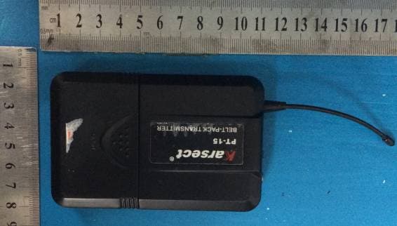
QSRPT-15
Apr 24, 2015Transmitter
Equipment Class
TBT - Licensed Broadcast Transmitter Worn on Body
QSRHT-25
Apr 22, 2015Transmitter
Equipment Class
TBF - Licensed Broadcast Transmitter Held to Face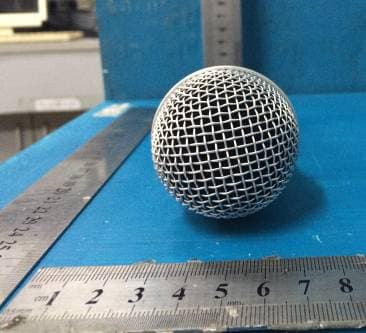
QSRHT-15
Apr 19, 2015Transmitter
Equipment Class
TBF - Licensed Broadcast Transmitter Held to Face
QSRHT-35A
Apr 19, 2015Transmitter
Equipment Class
TBF - Licensed Broadcast Transmitter Held to Face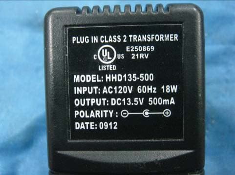
QSRKP1TA
Jun 20, 2014Monitor System
Equipment Class
DXX - Part 15 Low Power Communication Device Transmitter