QU7JPAAParking Sensor
Joyce Park Industrial Ltd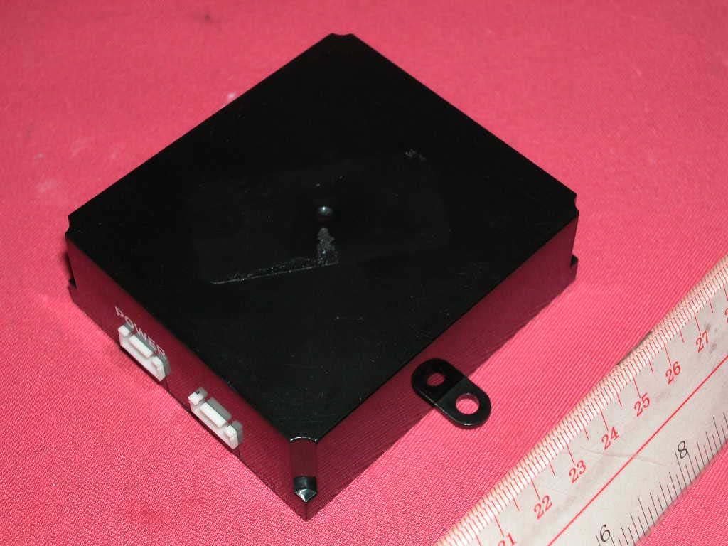
Click to zoom
Application Details
- Equipment Class
- DXX - Part 15 Low Power Communication Device Transmitter
- Date of Grant
- May 22, 2004
- Application Purpose
- Original Equipment
- Date of Application
- May 22, 2004
- Equipment Note
- Parking Sensor
- Frequency Range
- 915.00000000 - 915.00000000
- Company
- Joyce Park Industrial Ltd
- Country
- Hong Kong
Documents & Files
Document Text
Text extracted from the exhibit documents filed with the FCC. Open a document above to read the original.
External Photos
Test Setup FCC ID : QU7JPAA External Photo -front External Photo - rear
Internal Photos
Test Setup FCC ID : QU7JPAA Internal Photo – 1 Internal Photo - 2 Test Setup FCC ID : QU7JPAA Internal Photo – 3
Operational Description
Revision B2Page 1July 2003 TX4915 Low Power ASK Transmitter IC HiMARK Technology, Inc. reserves the right to change the product described in this datasheet. All information con- tained in this datasheet is subject to change without prior notice. HiMARK Technology, Inc. assumes no responsibility for the use of any circuits shown in this datasheet. Description The TX4915 is a low power ASK transmitter IC intended for applications in the North American and European VHF/UHF bands. The integrated voltage-controlled oscillator (VCO), phase/frequency detector, prescaler, and reference oscillator require only the addition of an external crystal to provide a complete phase-locked loop (PLL). In addi- tion to the standard power-down mode, the chip also includes an automatic lock-detect feature that disables the transmitter output when the PLL is out-of-lock. Features Output frequency range: 100 – 960 MHz Supply voltage range: 2.2 – 3.6 V Low current consumption with power down capability On-chip VCO with integrated PLL (÷ 64/128) dual modulus prescaler Out-of-lock inhibit circuit SSOP-16 package (0.64 mm pitch) Applications Wireless mouse Car alarm and home security systems Remote control systems Block Diagram 78 TXEN OSC OUT OSC IN 21 NC VSS2VCC2RESRES OSC VCO Prescaler ÷ 64/128 DO PFD and CP 3456 109 15 1614131211 VSSTXOUTVSS1VCC1MODIN AMP LD SW LD BIAS TX4915 Revision B2Page 2July 2003 Package and Pin Assignment SSOP-16 (0.64mm pitch) Symbol Dimensions in mmDimensions in inches min.nom.max.min.nom.max. A1.351.601.750.0530.0640.069 A10.10—0.250.004—0.010 A2—1.45——0.057— b0.200.250.300.0080.0100.012 C0.19—0.250.007—0.010 D4.80—5.000.189—0.197 E5.80—6.200.228—0.244 E13.80—4.000.150—0.157 e—0.64——0.025— L0.40—1.270.016—0.050 y——0.10——0.004 θ 0° — 8 °0° — 8 ° OSCIN OSCOUT TXEN VSS TXOUT VSS1 VCC1 MODIN SW LD DO RES RESB VREFP VSS2 VCC2 1 2 3 4 5 6 7 8 16 15 14 13 12 11 10 9 TX4915 HiMARK TX4915 Revision B2Page 3July 2003 Pin Descriptions NumberNameDescription 1OSCIN This pin is connected directly to the base of the reference oscillator transistor. The reference oscillator uses a modified Colpitts configuration. 2OSCOUTThis pin is connected directly to the emitter of the reference oscillator transistor. 3TXEN Transmitter enable control (TXEN = low = power down mode; TXEN = high = nor- mal operation mode). 4VSSGround connection for the transmit output amplifier. 5TXOUT Transmitter output. This pin is an open collector output and requires a pull-up inductor for bias/matching and a tapped capacitor network for matching. 6VSS1Ground connection for the transmit driver amplifier. 7VCC1Nominal supply voltage for the transmit driver amplifier. 8MODIN ASK modulation input. An external resistor, R MODIN , connected from the MODIN pin to supply voltage is used to bias the transmit amplifier chain. 9VCC2Nominal supply voltage for the VCO and PLL circuitry. 10VSS2Ground connection for the PLL circuitry. 11NCNo connection. 12RES Differential open collector VCO outputs. 13RES 14DO Output of the charge pump. An R-C network from this pin to ground is used to establish the PLL bandwidth. 15LD Lock detector output. This pin is used to set the threshold of the lock detect circuitry which enables or disables the transmit amplifier. A shunt capacitor should be used to set an R-C time constant with the on-chip series 1 KΩ resistor. The time constant should be set to approximately 15 times the reference period. 16SWPrescaler modulus control input (SW = high = ÷ 64; SW = low = ÷ 128). TX4915 Revision B2Page 4July 2003 Absolute Maximum Ratings V SS , V SS1 , V SS2 = 0V Recommended Operating Conditions V SS , V SS1 , V SS2 = 0V ParameterRatingUnit Supply voltage range–0.3 to +3.6V Power-down voltage –0.3 to V CC V MODIN voltage–0.3 to +1.1V Operating ambient temperature–40 to +85°C Storage temperature–40 to +150°C ParameterSymbol Va l u e Unit min.typ.max. Supply voltage range V CC 2.23.03.6V Operating temperature T A –10+25+60 o C TX4915 Revision B2Page 5July 2003 Electrical Characteristics (V CC = 3 V, V SS , V SS1 , V SS2 = 0 V, TXEN = high, T A = 25 °C, and f RF = 433.92 MHz unless otherwise noted) ParameterSymbolCondition Va l u e Unit min.typ.max. Power supply Supply voltageV CC 2.23.03.6V Total dc current (normal operation) I CC 50% duty cycle, 10 KHz data applied to the MODIN pin (R MODIN = 10 KΩ) 10.5mA Total dc current (power-down mode) I standby TXEN = low1μA Overall RF input frequency rangef RF 100960MHz ModulationASK Modulation frequency f MOD 100KHz Output power P OUT 50Ω load18dBm ON/OFF ratio70dB PLL Prescaler divide ratioSW = high = ÷ 64 SW = low = ÷ 128 64128 VCO gain K VCO Frequency and board layout dependent 20MHz/V Phase noise 10 KHz offset, 50 KHz loop BW–80dBc/Hz 100 KHz offset, 50 KHz loop BW–89dBc/Hz 2nd harmonic–30dBc 3rd harmonic–40dBc Reference frequency7MHz Crystal frequency spurs50 KHz PLL loop BW–50dBc Charge pump currentI CP -100100μA Stand-by mode control Transmitter enable/disable voltage TXEN = high = normal operation Vcc – 0.3 V V TXEN = low = power-down mode0.3V Turn-on time12ms Turn-off time12ms TX4915 Revision B2Page 6July 2003 Functional Description The TX4915 is a low-power ASK transmitter IC designed for applications operating within the frequency range of 100 to 960 MHz. In particular, it is intended for transmitter applications in 315/433 MHz band remote keyless entry and 868/915 MHz ISM-band systems. In addition, the TX4915 possesses a PLL-only mode which allows it to be simply used as a local oscillator source. The integrated voltage-controlled oscil- lator (VCO), phase/frequency detector, prescaler, and reference oscillator require only the addition of an external crystal to provide a complete phase-locked loop. In addition to the normal operation mode, the chip also includes an automatic lock-detect feature that disables the transmitter output when the PLL is out- of-lock. Reference crystal oscillator The OSCIN and OSCOUT inputs (pins 1 and 2) provide connections to an o…
Text truncated - open the document above for the full version.
Test Report
• The test results reported in this test report shall refer only to the sample actually tested and shall not refer or be deemed to refer to bulk from which such a sample may be said to have been obtained. • This report shall not be reproduced except in full without prior authorization from Intertek Testing Services Hong Kong Limited. • For Terms And Conditions of the services, it can be provided upon request. • The evaluation data of the report will be kept for 3 years from the date of issuance. Intertek Testing Services Hong Kong Ltd. 2/F., Garment Centre, 576 Castle Peak Road, Kowloon, Hong Kong. Tel: (852) 2173 8888 Fax: (852) 2371 0521 Website: www.hk.intertek-etlsemko.com Joyce Park Industrial Ltd. Application For Certification (FCC ID: QU7JPAA) Transmitter 0214478(S1) DL/Sandy May 18, 2004 INTERTEK TESTING SERVICES FCC ID: QU7JPAA i LIST OF EXHIBITS INTRODUCTION EXHIBIT 1: General Description EXHIBIT 2: System Test Configuration EXHIBIT 3: Emission Results EXHIBIT 4: Equipment Photographs EXHIBIT 5: Product Labelling EXHIBIT 6: Technical Specifications EXHIBIT 7: Instruction Manual EXHIBIT 8: Miscellaneous Information INTERTEK TESTING SERVICES FCC ID: QU7JPAA ii MEASUREMENT/TECHNICAL REPORT Joyce Park Industrial Ltd. - MODEL: SE-8100 SE-7100 SE-6100 FCC ID: QU7JPAA May 18, 2004 This report concerns (check one:) Original Grant X Class II Change Equipment Type: Low Power Transmitter (example: computer, printer, modem, etc.) Deferred grant requested per 47 CFR 0.457(d)(1)(ii)?Yes No X If yes, defer until: date Company Name agrees to notify the Commission by: date of the intended date of announcement of the product so that the grant can be issued on that date. Transition Rules Request per 15.37? Yes No X If no, assumed Part 15, Subpart C for intentional radiator - the new 47 CFR [12-08-03 Edition] provision. Report prepared by: Derek Leung Intertek Testing Services 2/F., Garment Center, 576, Castle Peak Road, HONG KONG. Phone: 852-2173-8504 Fax: 852-2371-0521 INTERTEK TESTING SERVICES FCC ID: QU7JPAA iii Table of Contents 1.0 General Description............................................................................................. 2 1.1 Product Description............................................................................................. 2 1.2 Related Submittal(s) Grants................................................................................. 2 1.3 Test Methodology................................................................................................ 3 1.4 Test Facility......................................................................................................... 3 2.0 System Test Configuration .................................................................................. 5 2.1 Justification ......................................................................................................... 5 2.2 EUT Exercising Software ..................................................................................... 5 2.3 Special Accessories ............................................................................................ 5 2.4 Equipment Modification ....................................................................................... 6 2.5 Measurement Uncertainty.................................................................................... 6 2.6 Support Equipment List and Description.............................................................. 6 3.0 Emission Results ................................................................................................. 8 3.1 Field Strength Calculation.................................................................................... 9 3.2 Radiated Emission Configuration Photograph .................................................... 11 3.3 Radiated Emission Data .................................................................................... 12 4.0 Equipment Photographs .................................................................................... 15 5.0 Product Labelling............................................................................................... 17 6.0 Technical Specifications .................................................................................... 19 7.0 Instruction Manual .............................................................................................. 21 8.0 Miscellaneous Information................................................................................. 23 8.1 Bandwidth Plot .................................................................................................. 24 8.2 Emissions Test Procedures............................................................................... 25 INTERTEK TESTING SERVICES FCC ID: QU7JPAA iv List of attached file Exhibit type File Description filename Test Report Test Report report.pdf Operation Description Technical Description descri.pdf Test Setup Photo Radiated Emission radiated photos.doc Test Report Bandwidth Plot bw.pdf External Photo External Photo external photos.doc Internal Photo Internal Photo internal photos.doc Block Diagram Block Diagram block.pdf Schematics Circuit Diagram circuit.pdf ID Label/Location Label Artwork and Location label.pdf User Manual User Manual manual.pdf INTERTEK TESTING SERVICES FCC ID: QU7JPAA 1 EXHIBIT 1 GENERAL DESCRIPTION INTERTEK TESTING SERVICES FCC ID: QU7JPAA 2 1.0 General Description 1.1 Product Description The Equipment Under Test (EUT) is a Transmitter Part of a Parking Sensor operating at 915MHz. The EUT is powered by 12V d.c. It will install on a car according to installation instruction. When the driver select reverse gear, the EUT will sound a beep. This indicates that the Parking Sensor is working and has been activated. It transmits signal to the corresponding receiver. It help driver to prevent crash alongside the vehicle or behind. Antenna Type : Integral, Internal The Model: SE-6100 and SE-7100 are the same as the Model: S…
Text truncated - open the document above for the full version.
Test Setup Photos
Test Setup FCC ID : QU7JPAA Radiated -front Radiated - rear 0214478(S1) 0214478(S1)
Contact Information
Applicant
Mansfield Lam(Mr)
Technical Contact
Intertek Testing Services Hong Kong Ltd.Derek Leung
[email protected]852-2173-8539
2/F., Garment Centre, · Kowloon · Hong Kong
Non-Technical Contact
Intertek Testing Services Hong Kong Ltd.Derek Leung
[email protected]852-2173-8539
Test Firm
Intertek Testing Services Hong KongBilly Chow
Technical Specifications
| # | Rule Parts | Frequency Range | Power Output |
|---|---|---|---|
| 1 | 15C | 915 MHz - 915 MHz | - |
Other Applications from Joyce Park Industrial Ltd
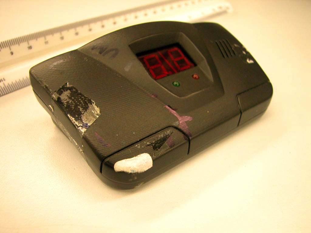
QU7JPAR
May 22, 2004Parking Sensor
Equipment Class
CYY - Communications Receiver used w/Pt 15 Transmitter