R74TC3000U0FM Handheld Transceiver
Shenzhen HYT Science &Technology Co Ltd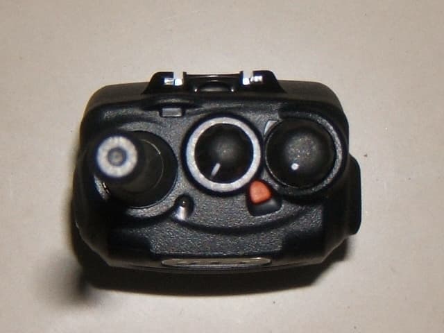
Click to zoom
Application Details
- Equipment Class
- TNF - Licensed Non-Broadcast Transmitter Held to Face
- Date of Grant
- May 20, 2007
- Application Purpose
- Original Equipment
- Date of Application
- May 20, 2007
- Equipment Note
- FM Handheld Transceiver
- Frequency Range
- 406.10000000 - 470.00000000
- Country
- China
Documents & Files
Document Text
Text extracted from the exhibit documents filed with the FCC. Open a document above to read the original.
Users Manual
1 THANK YOU! We are grateful for your purchase of HYT product. We believe this easy–to-use radio will provide you with dependable and reliable communications. This HYT portable two-way radio is a precision device. Treat it with care, and you will enjoy years of reliable operation. MODELS COVERED IN THIS MANUAL TC3000 VHF Radio TC3000 UHF Radio 2 Contents User Safety, Training, and General Information Compliance with RF Energy Exposure Standards Important Note: FCC Information FCC Compliance Precautions Product Inspection Battery Information Accessory Installation Battery Antenna Belt Clip Earplug Cover External Earphone/Microphone (optional) Getting Started Features and Operation Turn on/off the radio Adjust the Volume Select Channel Transmit Receive Monitor Repeater/Talk Around Repeater/ Reverse Frequency Selectable Power Scan Music Call Emergency ANI/Emergency Siren VOX Feature Built-in Modem Low Battery Alert 2-Tone/HDC1200 Selective Call Troubleshooting Guide Care and Cleaning Optional Accessories Frequency Chart 3 User Safety, Training, and General Information READ THIS IMPORTANT INFORMATION ON SAFE AND EFFICIENT OPERATION BEFORE USING YOUR HYT PORTABLE TWO-WAY RADIO. Compliance with RF Energy Exposure Standards Your HYT two-way radio is designed and tested to comply with a number of national and international standards and guidelines (listed below) regarding human exposure to radio frequency electromagnetic energy. This radio complies with the IEEE (FCC) and ICNIRP exposure limits for occupational/controlled RF exposure environment at duty cycles of up to 50% talk-50% listen and should be used for occupational use only. In terms of measuring RF energy for compliance with the FCC exposure guidelines, your radio radiates measurable RF energy only while it is transmitting (during talking), not when it is receiving (listening) or in standby mode. Note: The approved batteries supplied with this radio are rated for a 5-5-90 duty cycle (5% talk-5% listen-90% standby), even though this radio complies with the FCC occupational RF exposure limits at duty cycles of up to 50% talk. Your HYT two-way radio complies with the following of R F e n e r g y exposure standards and guidelines: z United States Federal Communications Commission, Code of Federal Regulations; 47CFR part 2 sub-part J z American National Standards Institute (ANSI)/Institute of Electrical and Electronic Engineers (IEEE) C95. 1-1992 z Institute of Electrical and Electronic Engineers (IEEE) C95. 1-1999 Edition z International Commission on Non-Ionizing Radiation Protection (ICNIRP) 1998 Operational Instructions and Training Guidelines To ensure optimal performance and compliance with the occupational/controlled environment RF energy exposure limits in the above standards and guidelines, users should transmit no more than 50% of the time and always adhere to the following procedures: Transmit and Receive To transmit (talk), push the Push-To-Talk (PTT) button; to receive, release the PTT button. Hand-held radio operation Hold the radio in a vertical position with the microphone one to two inches (2.5 to 5 cm) away from the lips. 4 Body-worn operation z Always place the radio in an HYT approved clip, holder, holster, case, or body harness for this product. Use of non-HYT-approved accessories may exceed FCC RF exposure guidelines. Antennas & Batteries Use only HYT approved, supplied antenna or HYT approved replacement antenna. Unauthorized antennas, modifications, or attachments could damage the radio and may violate FCC regulations. z Use only HYT approved, supplied batteries or HYT approved replacement batteries. Use of non- HYT -approved batteries may exceed FCC RF exposure guidelines. Approved Accessories For a list of HYT approved accessories, see the accessories page of this user manual or visit the following website which lists approved accessories: http://www.hty.com.cn 5 Important note: FCC Information FCC Compliance This equipment has been tested and found to comply with the limits for a Class B digital device, pursuant to part 15 of the FCC Rules. These limits are designed to provide reasonable protection against harmful interference in a residential installation. This equipment generates, uses and can radiate radio frequency energy and, if not installed and used in accordance with the instructions, may cause harmful interference to radio communications. However, there is no guarantee that interference will not occur in a particular installation. If this equipment does cause harmful interference to radio or television reception, which can be determined by turning the equipment off and on, the user is encouraged to try to correct the interference by one or more of the following measures: 6 Reorient or relocate the receiving antenna. Increase the separation between the equipment and receiver. Connect the equipment into an outlet on a circuit different from that to which the receiver is connected. Consult the dealer or an experienced radio/TV technician for help. FCC Requirements Your radio must be properly licensed Federal Communications Commission prior to use. Your HYT Wireless dealer can assist you in meeting these requirements. Your dealer will program each radio with your authorized frequencies, signaling codes, etc., and will be there to meet your communications needs as your system expands. Precautions • Only qualified technicians are allowed to maintain this product. • Do not use the radio or charge a battery in explosive areas such as coal gas, dust, steam, etc. • Switch OFF the radio while refueling or parking at gas station. • Do not modify or adjust this radio without permission. • Do not expose the radio to direct sunlight over a long time, nor place it close to heating source. • Do not place the radio in excessively dusty, humid areas, nor on unstable surfaces. • Stubby antenna especially suits communication in close quarters, while long and fine antenna provides better communication quality and avoids any …
Text truncated - open the document above for the full version.
Block Diagram
1 2 3 4 5 6 ABCD 6 5 4 3 2 1 D CBA Title Number Revision Size C Date: 15-Sep-2004 Sheet of File: D:\TC265 365\Service Manual\material\TC3000~13.DDB Drawn By: ANT LPF ANT SW D101 MA2Z077 FINAL AMP Q107 2SK2595 DRIVE AMP Q105 2SK2596 APCIC100 NJM2904V 5T SWQ109 DTA144EE SW Q106 2SK1824 SW Q108 DTC114EE 5T 5T Q110 DTC114TE THERMALPROTECTION APC/TV B+ B+/SWQ104Q103 2SK1824FMMT717 DET AMPQ102 2SC4988 5T 5T AMPQ101 2SC5108 LO SWD100,D103MA2S077 *2 BUFF AMP Q310 2SC5108(Y) 5C VCO Q308 2SC4617(S)RIPPLE FILTER 5C T/R FILTERLOOP Q416 2SC5108(Y) BUFF AMP PLL LOCK PLL_CLKPLL_ENPLL_DATA X40116.8MHz VCXO MB MOD IC400 SA7026 ANT SW D201D202 MA2S077 *2 BPFL201,L202C20,C203,C204D206,D207HVC350B*2 AMPQ224 AT-41511 5R BPFL206,L207C213,C216,C217D204,D205HVC350B*2 LPF L215L217 1st MIX IC218 HSMS-2827 XF201 44.85MHz MCF Q222 2SC5108(Y)IF AMP 5R CF201455KHz X202 44.395MHz CD201455KHz MIXO IFI FM IF SYSTEM IC204 TA31136FN DC SW Q226DTA114EE SQL RSSI D601 RB706F LIMITTER X601 18.432MHz BASEBAND PROCESSOR IC601 CMX881 AF DET DTMF DECODE DTMF_DATA DTMF_STD DTMF_CLK DTMF_PD IC602 LC73872M EN0EN2EN1EN3 5CNS VOL D1 1SR154-400 PROTECT FUSE + - BATT7.5V AVRIC505 XC6201P502R 5M AVR TK11250CM IC9 5C RESET DC SW Q4 2SJ243 SAVE IC503RN5VL42AA AVR NJU7201U50 IC6 DC SW Q2 2SJ243 DC SW Q3 2SA1745 5TC5T5RC5R SWB+ B+ MICROPROCESSOR IC500 30622M4102GP X500 9.8304MHz IC502 IS24C08-3GT EEPROM SCLSDA BATT RET A0--A18D0--D7CEOEWE IC17 AT29C020 BBP_IRQNBBP_RPL PB1 PB2 PB3 PB4 SW SW Q6 2SC5343 Q5 2SC5343 SWB+ LR LG SP MIC SW Q7002SJ243 AF PA IC710 TDA8547TS SW Q710DTC114YE B+ MIC MIC AF DET MODMB SWB+ SWB+ AUDIO_EN 5RC5TC Ver APC/TV DTMF_CLKDTMF_PDTXD COM_SWBBP_CMDBBP_CSNBBP_CLK BBP_RPL T/RAUDIO_ENSAVELGLR PLL_ENPLL_DATAPLL_CLK EN0EN1EN2EN3LOCKVOLRSSI RXDDTMF_STDDTMF_DATAOPTION TC3000UHF EXT_SPK+EXT_SPK- OPT_B+ EXT_MIC OPT_SEL2OPT_SEL1 GNDRXDTXD RSSI NC OPTION EXT_MIC_SEL SWB+EXT_SP_SELPTTRXDTXDRSSIOPTION PROTECT D720EDZ6.8B 5CNS PB1PB2PB3PB4 5R 5C 5C 5C W/N BBP_IRQN EXP_SW BBP_CSNBBP_CMDBBP_CLK Q701UPA672T SW EXT_MIC_SEL PROTECTD721EDZ6.8B PROTECTD719EDZ6.8B EXT_SP_SEL EXT_MIC_SEL CF202455KHzCF(W) CF(N) D217DAN222 D215DAN222 RF SW RF SW Q206 DTA144EE Q207 DTC144EE W/N FLASH X6023.57954MHz 5CNS 5CNS IC605 TA75S01F BUFFER Ver MB PTT Vbias 5M COMPANDER IC603SA575 SW COM_SW MAX4636 EXP EXP_SW IC604 MOD MOD MB COMPRESSOR EXPANDER DTMF AF PA MIC_FB AUDIO Q216 2SC3356 AMP 5R 5TC SWCOM IC606TC75W51FU AMP Vbias CTCi IC611 TA75W01F FILTER
External Photos
SHENZHEN HUATONGWEI INTERNATIONAL INSPECTION CO., LTD REPORT NO: WE06090008 FCC ID: R74TC3000U0 IC: 5465A-TC3000U0 DATE: 12/05/2006 Pag57 Rev. 00 Top view of EUT Bottom view of EUT SHENZHEN HUATONGWEI INTERNATIONAL INSPECTION CO., LTD REPORT NO: WE06090008 FCC ID: R74TC3000U0 IC: 5465A-TC3000U0 DATE: 12/05/2006 Pag58 Rev. 00 Right view of EUT Left view of EUT SHENZHEN HUATONGWEI INTERNATIONAL INSPECTION CO., LTD REPORT NO: WE06090008 FCC ID: R74TC3000U0 IC: 5465A-TC3000U0 DATE: 12/05/2006 Pag59 Rev. 00 Front view of EUT Back view of EUT
ID Label/Location Info
Applicant: SHENZHEN HYT SCIENCE &TECHNOLOGY CO., LTD. FCC ID: R74TC3000U0 IC: 5465A-TC3000U0 Model Name: TC3000-U(0) Applicant: SHENZHEN HYT SCIENCE &TECHNOLOGY CO., LTD. FCC ID: R74TC3000U0 IC: 5465A-TC3000U0 The FCC identifier is marked in the product label and the RF exposure caution label is attached on the rear side of the cabinet. The user notice and warning statement are described in the user manual. . Proposed Label Location on EUT
Internal Photos
SHENZHEN HUATONGWEI INTERNATIONAL INSPECTION CO., LTD REPORT NO: WE06090008 FCC ID: R74TC3000U0 IC: 5465A-TC3000U0 DATE: 12/05/2006 Pag60 Rev. 00 Detached view of EUT-1 Detached view of EUT-2 SHENZHEN HUATONGWEI INTERNATIONAL INSPECTION CO., LTD REPORT NO: WE06090008 FCC ID: R74TC3000U0 IC: 5465A-TC3000U0 DATE: 12/05/2006 Pag61 Rev. 00 Detached view of EUT-3
Operational Description
TC3000 Circuit Description 第 9 页 共 34 页 Circuit Description 1. Power Supply Power supply of the radio is derived from the battery, which supplies battery B+ after passing through fuse 3A and then feeds through power switch. The power supplies voltage for three AVRs. IC505 supplies 5V (5M) voltage for the control circuit. IC9 supplies 5V (5C) voltage for the shared circuit. And IC6 supplies voltage for the transmit/receive circuit. In transmit mode, 5TC becomes low voltage and Q3 is turned on to supply 5V (5T) voltage for the transmit circuit. In receive mode, 5RC becomes low voltage and Q2 is turned on to supply 5V (5R) voltage for the receive circuit. BATTFUSE PROTECT 5C 5M BUFF 1/2BIA S AVR AVR SW 5R 5T AVR SW SW SAVE 5RC 5TC Fig. 1 Power Supply Block Diagram 2. PLL Frequency Synthesizer PLL circuit generates the first local oscillator signal for reception and RF signal for transmission. CPU Q416 UL X401 IC400 PLL IC500 CV CLK,DAT,EN TCXO VCO BUFFSW MB D100 T/R To Drive Amp BUFF D103 SW To Mixer Q310 Fig2. PLL circuit 1) PLL IC400 is fractional divider. Step frequency of PLL circuit is 2.5KHz or 6.25KHz. A 16.8MHz reference oscillator signal is divided at IC400 by a fixed counter to generate a 2.5KHz or 6.25KHz reference frequency. Output signal from VCO is buffer amplified by Q416 and divided at IC400 by a frequency divider. Divided signal is compared in the phase comparator with 2.5 KHz or 6.25KHz reference signal of IC400. Output signal from phase comparator is filtered through a low pass filter and passed to the VCO to control oscillator frequency. TC3000 Circuit Description 第 10 页 共 34 页 2) VCO The operating frequency is generated by Q352 in transmit mode and by Q350 in receive mode. Operating frequency generates a control voltage by phase comparator to control varactor diodes so that the oscillator frequency is consistent with the MCU preset frequency (D350, D352, D354 and D355 in transmit mode and D351, D353, D356 and D357 in receive mode). T/R pin is set high level in receive mode and low in transmit mode. The output from Q352 and Q350 is amplified by Q354 and sent to buffer amplifier. 3) Unlock Detector An unlock condition appears if low level appears at LOCK pin of IC400. Transmission is forbidden if this condition is detected by microprocessor. 3. Receiver The receiver utilizes double conversion superheterodyne. C ANT ANT SW BPFQ201 RF AMP BPF MCF XF201 IF AMP Q222 MIXER IC218 CF201,202 IF,MIX,DET IC204 AF AMP IC720SP 1st Local OSC (PLL) 2nd Local OSC IF AMP Q216 Fig.3 Receiver Section Configuration 1) Front-end Amplifier The signal from antenna is amplified at RF amplifier (Q201) after passing through a transmit/receive switch circuit and a band pass filter. The amplified signal is filtered through a band pass filter to remove unwanted signals before it passes the first mixer. 2) First Mixer The signal from RF amplifier is mixed with the first local oscillator signal from PLL frequency synthesizer circuit at the first mixer (IC218) to create a 44.85MHz first IF signal. The first IF signal is then fed through a crystal filter (XF201) to further remove spurious signals from adjacent channel. 3) IF Amplifier The first IF signal is amplified by Q216 before passing through crystal filter and by Q222 after crystal filter and then enters IF processing chip IC204. The signal is mixed with the second local oscillator signal again in IC204 to create a 455KHz second IF signal. The second IF signal then passes through a 455KHz ceramic filter (wideband: CF201/narrowband: CF202) to eliminate unwanted signals before it is amplified and detected in IC204. 4) Narrowband/Wideband Switch Circuit Turn on ceramic filter CF201 (wideband)/CF202 (narrowband) to set each channel as wideband or narrowband. W/N pin of IC500 outputs wideband (high level) and narrowband (low level) signal. 5) AF Amplifier The result AF signal from IC204 is amplified by IC606, and then passes through AF processing chip IC601 and compander IC603. The processed AF signal is then amplified by an AF power amplifier (IC720) to drive the speaker. TC3000 Circuit Description 第 11 页 共 34 页 4. Transmitter 1) AF and Signaling Modulating signal from the microphone passes through Q700 switch and compander IC603 before it enters AF processing chip IC601. CPU generates CTCSS/CDCSS signaling and IC601 produces DTMF/2-Tone/5-Tone signaling, which then pass through MOD and enter VCO together with the modulating signal for direct FM modulation. (See fig.5) 2) RF Amplifier The transmit signal from VCO buffer amplifier (Q310) is amplified by Q101 and Q102. The amplified signal is then amplified by the power amplifier Q105 and Q107 (include a two-stage FET amplifier) to create 4.0W RF power. (See fig.4) D C B A Title AMP Q101.102 5T DRIVE AMP Q105 FINAL AMP Q107 ANT SW D101LPF ANT ANT SW D201.202 RX Q106 SW Q109 SW 5T IC100 APC DET Q103.Q104 B SW B APC 5T TH101 SW Q110 5T Q108 SW 5TC Fig.4 APC System 3) Antenna Switch and LPF Output signal from RF amplifier passes through a low-pass filter network and a transmit/receive switch circuit comprised of D101, D201 and D202 before it reaches the antenna terminal. D201 and D202 is turned on (conductive) in transmit mode and off (isolated) in receive mode. 4) APC The automatic power control (APC) circuit stabilizes the transmit output power by detecting the drain current of final stage amplifier FET. IC100 (2/2) compares the preset reference voltage with the voltage obtained from final current. APC voltage is proportional to the difference between auto detect voltage and reference voltage output from IC100 (1/2). The output voltage controls FET power amplifier and keeps the transmitter output power constant. The output voltage can be varied by the microprocessor, which hence controls the transmitter output power. TC3000 Circuit Description 第 12 页 共 34 页 5. Signalling Section The block diagram of signaling section is shown as figure 5. D601 LIMITTER X601 BASEBAND PROCESSOR IC601 BBP_IRQN BBP_RPL SP MI…
Text truncated - open the document above for the full version.
Parts List/Tune Up Info
No.Material No.Material NameQty.Ref.No. Address Remarks 13101051030020Chip capacitor 0402 0.01UF K 25V1C501B1C 23101051030020Chip capacitor 0402 0.01UF K 25V1C502B2B 33101051030020Chip capacitor 0402 0.01UF K 25V1C503B3B 43101052700000Chip capacitor 0402 27PF J 50V1C504T3C 53101051030020Chip capacitor 0402 0.01UF K 25V1C505T3C 63101052700000Chip capacitor 0402 27PF J 50V1C506T3C 73101051010030Chip capacitor 0402 100PF J 50V1C507B4B 83101051010030Chip capacitor 0402 100PF J 50V1C508B4B 93101051010030Chip capacitor 0402 100PF J 50V1C509B4B 103101051010030Chip capacitor 0402 100PF J 50V1C510B4C 113101051010030Chip capacitor 0402 100PF J 50V1C511B4C 123101054710010Chip capacitor 0402 470PF K 50V1C512B4B 133101051010030Chip capacitor 0402 100PF J 50V1C514B4B 143101051010030Chip capacitor 0402 100PF J 50V1C515B4B 153101051010030Chip capacitor 0402 100PF J 50V1C516B4B 163101051010030Chip capacitor 0402 100PF J 50V1C517B4C 173101051010030Chip capacitor 0402 100PF J 50V1C518B4C 183101051010030Chip capacitor 0402 100PF J 50V1C519B4B 193101051010030Chip capacitor 0402 100PF J 50V1C522B4B 203101051010030Chip capacitor 0402 100PF J 50V1C523B4B 213101051010030Chip capacitor 0402 100PF J 50V1C524B4B 223101051010030Chip capacitor 0402 100PF J 50V1C525B4B 233101051010030Chip capacitor 0402 100PF J 50V1C526B4B 243101051010030Chip capacitor 0402 100PF J 50V1C527B4B 253101051010030Chip capacitor 0402 100PF J 50V1C528B4B 263101051010030Chip capacitor 0402 100PF J 50V1C530B4B 273101051010030Chip capacitor 0402 100PF J 50V1C531B4B 283101051010030Chip capacitor 0402 100PF J 50V1C532B4B 293101051010030Chip capacitor 0402 100PF J 50V1C533B4B 303101051010030Chip capacitor 0402 100PF J 50V1C534B4B 313101051010030Chip capacitor 0402 100PF J 50V1C535B4B 323101051010030Chip capacitor 0402 100PF J 50V1C536B4B 333101054710010Chip capacitor 0402 470PF K 50V1C553B3C 343101054710010Chip capacitor 0402 470PF K 50V1C554B3C 353101054710010Chip capacitor 0402 470PF K 50V1C555B3C 363104074750030Ta-capacitor 0805 4.7UF M 10V1C556B3C 373101054710010Chip capacitor 0402 470PF K 50V1C557B3C 383101051030020Chip capacitor 0402 0.01UF K 25V1C558B3B 393101054710010Chip capacitor 0402 470PF K 50V1C559B3B 403101052730000Chip capacitor 0402 0.027UF K1C560B3B 413101052730000Chip capacitor 0402 0.027UF K1C561B2C 423101054710010Chip capacitor 0402 470PF K 50V1C570B2C 433104074750030Ta-capacitor 0805 4.7UF M 10V1C571B2C 443101054710010Chip capacitor 0402 470PF K 50V1C572B2C 453101054710010Chip capacitor 0402 470PF K 50V1C573B2C 463101051050010Chip capacitor 0402 1UF Z 6.3V1C601B3C TC3000UHF Part List 1 (Control Board) 确认人:接收时间:确认时间: 473101051010030Chip capacitor 0402 100PF J 50V1C603T2B 483101051040040Chip capacitor 0402 0.1UF K 10V1C604B2C 493101051040040Chip capacitor 0402 0.1UF K 10V1C605B2C 503101051030020Chip capacitor 0402 0.01UF K 25V1C609T2B 513104071060010Ta-capacitor 0805 10UF M 10V1C610T2B 523104071560020Ta-capacitor 0805 15UF M 6.3V1C611B2C 533101051040040Chip capacitor 0402 0.1UF K 10V1C613B2C 543101051040040Chip capacitor 0402 0.1UF K 10V1C614B1C 553101051030020Chip capacitor 0402 0.01UF K 25V1C615B1D 563104071060010Ta-capacitor 0805 10UF M 10V1C616B1C 573101054710010Chip capacitor 0402 470PF K 50V1C617T2B 583104071560020Ta-capacitor 0805 15UF M 6.3V1C618T1B 593101051050010Chip capacitor 0402 1UF Z 6.3V1C620T1B 603104072250010Ta-capacitor 0805 2.2UF M 10V1C625T2B 613104071060010Ta-capacitor 0805 10UF M 10V1C626B1C 623101051050010Chip capacitor 0402 1UF Z 6.3V1C627T2B 633101051040040Chip capacitor 0402 0.1UF K 10V1C628B3C 643104071060010Ta-capacitor 0805 10UF M 10V1C629B1B 653101051010030Chip capacitor 0402 100PF J 50V1C630B3C 663101051040040Chip capacitor 0402 0.1UF K 10V1C632B2D 673104072250010Ta-capacitor 0805 2.2UF M 10V1C633B3C 683104071060010Ta-capacitor 0805 10UF M 10V1C634T2B 693101051050010Chip capacitor 0402 1UF Z 6.3V1C636B2D 703101052710000Chip capacitor 0402 270PF J 50V1C638B2D 713101051020010Chip capacitor 0402 1000PF K 50V1C640T2A 723101054700010Chip capacitor 0402 47PF J 50V1C642B2D 733101051030020Chip capacitor 0402 0.01UF K 25V1C645B2D 743101051010030Chip capacitor 0402 100PF J 50V1C646B3C 753101054710010Chip capacitor 0402 470PF K 50V1C647B3C 763104074750030Ta-capacitor 0805 4.7UF M 10V1C648B3C 773101051030020Chip capacitor 0402 0.01UF K 25V1C649B3C 783101051030020Chip capacitor 0402 0.01UF K 25V1C650B3C 793101051040040Chip capacitor 0402 0.1UF K 10V1C651B3C 803101053330000Chip capacitor 0402 0.033UF K1C652B3C 813101053330000Chip capacitor 0402 0.033UF K1C654B3C 823104071060010Ta-capacitor 0805 10UF M 10V1C655T2B 833101053330000Chip capacitor 0402 0.033UF K1C657T2B 843101051030020Chip capacitor 0402 0.01UF K 25V1C658B1C 853101051040040Chip capacitor 0402 0.1UF K 10V1C660B1C 863101056830000Chip capacitor 0402 0.068UF K1C661B1C 873101061050060Chip capacitor 0603 1UF K 10V1C663B1C 883101053320010Chip capacitor 0402 3300PF K 50V1C664B1C 893101053310020Chip capacitor 0402 330PF K 50V1C665B1C 903101051030020Chip capacitor 0402 0.01UF K 25V1C666B1C 913101051050010Chip capacitor 0402 1UF Z 6.3V1C667B3C 923101053320010Chip capacitor 0402 3300PF K 50V1C668B3C 933101051020010Chip capacitor 0402 1000PF K 50V1C669B3C 943101053330000Chip capacitor 0402 0.033UF K1C670B3C 确认人:接收时间:确认时间: 953101055620000Chip capacitor 0402 5600PF K 25V1C671B4C 963104074750030Ta-capacitor 0805 4.7UF M 10V1C673B3C 973101051050010Chip capacitor 0402 1UF Z 6.3V1C674B3D 983101051050010Chip capacitor 0402 1UF Z 6.3V1C675B4D 993101051030020Chip capacitor 0402 0.01UF K 25V1C676B3C 1003101051040040Chip capacitor 0402 0.1UF K 10V1C677B4C 1013101051020010Chip capacitor 0402 1000PF K 50V1C678B4C 1023101056830000Chip capacitor 0402 0.068UF K1C679B4C 1033101053330000Chip capacitor 0402 0.033UF K1C680B4D 1043101051050010Chip capacitor 0402 1UF Z 6.3V1C681B4D 1053101051050010Chip capacitor 0402 1UF Z 6.3V1C682B4D 1063101061050060Chip capacitor 0603 1UF K 10V1C683B3D 1073104071560020Ta-capacitor 0805 15UF M 6.3V1C685B3C 1083104071560020Ta-capacitor 0805 15UF M 6.…
Text truncated - open the document above for the full version.
RF Exposure Info
Report No: SZ07010044S01 Page 3 of 46 Contents 1. GENERAL CONDITIONS 2. ADMINISTRATIVE DATA 2.1. Identification of the Responsible Testing Laboratory 2.2. Identification of the Responsible Testing Location(s) 2.3. Organization Item 2.4. Identification of Applicant 2.5. Identification of Manufacture 3. EQUIPMENT UNDER TEST (EUT) 3.1. Identification of the Equipment under Test 3.2. Identification of all used Test Sample of the Equipment under Test 4. OPERATIONAL CONDITIONS DURING TEST 4.1. Schematic Test Configuration 4.2. SAR Measurement System 5. CHARACTERISTICS OF THE TEST 5.1. Applicable Limit Regulations 5.2. Applicable Measurement Standards 6. LABORATORY ENVIRONMENT 7. TEST RESULTS 7.1. Dielectric Performance 7.2. Summary of Measurement Results 7.3. Conclusion 8. MEASUREMENT UNCERTAINTY 9. MAIN TEST INSTRUMENTS This Test Report consists of the following Annexes: Annex A: Accreditation Certificate Annex B: Test Layout Annex C: Sample Photographs Annex D: Graph Test Results Annex E: System Performance Check Data Report No: SZ07010044S01 Page 4 of 46 1.GENERAL CONDITIONS 1.1 This report only refers to the item that has undergone the test. 1.2 This report standalone dose not constitute or imply by its own an approval of the product by the certification Bodies or competent Authorities. 1.3 This document is only valid if complete; no partial reproduction can be made without written approval of ShenZhen Morlab Communications Technology Co.,Ltd.. 1.4 This report cannot be used partially or in full for publicity and/or promotional purposes without previous written approval of ShenZhen Morlab Communications Technology Co.,Ltd. and the Accreditation Bodies, if it applies. 1.5 Body-worm operations are restricted to belt-clips, holsters or similar accessories that have no metallic component in the assembly and that provide at 1.5cm separation between the device, including its antenna, and the user’s body. Report No: SZ07010044S01 Page 5 of 46 2. Administrative Date 2.1. Identification of the Responsible Testing Laboratory Company Name: ShenZhen Morlab Communications Technology Co.,Ltd. Department: Testing Department Address: 3Fl, Electronic Testing Building, ShaHe Road, NanShan District, ShenZhen, P. R. China Telephone: +86-755-86130268 Fax: +86-755-86130218 Responsible Test Lab Managers: Mr. Shu Luan 2.2. Identification of the Responsible Testing Location(s) Company Name: ShenZhen Morlab Communications Technology Co.,Ltd. Address: 3Fl, Electronic Testing Building, ShaHe Road, NanShan District, ShenZhen, P. R. China 2.3. Organization Item Morlab Report No.: SZ07010044S01 Morlab Project Leader: Mr. Wu Xuewen Morlab Responsible for Accreditation scope: Mr. Shu Luan Start of Testing: 2007-01-13 End of Testing: 2007-04-03 2.4. Identification of Applicant Company Name: SHENZHEN HYT SCIENCE & TECHNOLOGY CO., LTD. Address: HYT Tower, Shenzhen Hi-Tech Industrial Park North, Beihuan Rd., Nanshan District, Shenzhen, P.R.C. Contact person: -- Telephone: -- Fax: -- 2.5. Identification of Manufacture Company Name: SHENZHEN HYT SCIENCE & TECHNOLOGY CO., LTD. Address: HYT Tower, Shenzhen Hi-Tech Industrial Park North, Beihuan Rd., Nanshan District, Shenzhen, P.R.C. Contact person: -- Telephone: -- Fax: -- Notes: This data is based on the information by the applicant. Report No: SZ07010044S01 Page 6 of 46 3. Equipment Under Test (EUT) 3.1. Identification of the Equipment under Test Brand Name: HYT Type Name: TC3000-U(0) /400-470MHz Marking Name: TC3000-U(0) /400-470MHz Test frequency 400-470MHz Development Stage Identical prototype Accessories Charger Battery Model BL1709 Battery specificationDC 7.4, 1700mAh Antenna type Build outside Operation mode PTT General description: Modulation mode 11K0F3E(2M+2D,M=3, D=2.5, Necessary Bandwidth= 11 KHz for 12.5 KHz) ; 16K0F3E(2M+2D,M=3, D=5, Necessary Bandwidth= 16 KHz for 25 KHz). NOTE: Specific Absorption Rate (SAR) is a measure of the rate energy absorption due to exposure to an RF transmitting source (wireless portable device). Report No: SZ07010044S01 Page 7 of 46 4 OPERATIONAL CONDITIONS DURING TEST 4.1 Schematic Test Configuration During SAR test, EUT is in Traffic Mode (Channel Allocated) at Normal Voltage Condition. A communication link is set up with a System Simulator (SS) by air link, and a call is established. The TCH is allocated to CH1 (400.064 MHz), CH2 (436.088 MHz) and CH3 (469.114 MHz).The EUT is commanded to operate at maximum transmitting power. The EUT shall use its internal transmitter. The antenna(s), battery and accessories shall be those specified by the manufacturer. The EUT battery must be fully charged and checked periodically during the test to ascertain uniform power output. If a wireless link is used, the antenna connected to the output of the base station simulator shall be placed at least 50 cm away from the handset. The signal transmitted by the simulator to the antenna feeding point shall be lower than the output power level of the handset by at least 35 dB. 4.2 SAR Measurement System The SAR measurement system being used is the IndexSAR SARA2 system, which consists of a Figure1. SAR Lab Test Measurement Set-up Mitsubishi RV-E2 6-axis robot arm and controller, IndexSAR probe and amplifier and SAM phantom Report No: SZ07010044S01 Page 8 of 46 Head Shape. The system is controlled remotely from a PC, which contains the software to control the robot and data acquisition equipment. The software also displays the data obtained from test scans. In operation, the system first does an area (2D) scan at a fixed depth within the liquid from the inside wall of the phantom. When the maximum SAR point has been found, the system will then carry out a 3D scan centred at that point to determine volume averaged SAR level. 4.2.1 Robot system specification The robot is used to articulate the probe to programmed positions inside the phantom head to obtain the SAR readings from the DUT. 4.2.2 Probe and amplifier specification IXP-050 Indexsar isotropic immer…
Text truncated - open the document above for the full version.
Schematics
L20522n L2015T L2025T R204100K R202100K L2065T L2075T R220100K R207100K R222100K C219100p C206 NC C2127p *C216 C2800.01u C2187.5p *C201 *C203 C20520p C2029p C2049p C211NC *C213 C2179p C210a0.1u FILI 8 FILO DEC IFI VCC MIXO OSCO OSCI 1 MIXI 16 E NREC NDET RSSI IFO QUAD AF 9 IC204 TA31136FN R297 18K C239180p C233 82p R2082.2K CD201455K C2320.01u C238 0.1u R201 100K C2410.1u C231 33p R299680K R206 2.7K R294 470 C225 0.01u C2480.1u C2420.1u SQL RSSI AF DET 5R Q226 DTA114EE XF20144.85MHz C278470p C2697p L21715n L21515n C26812p C2614p R22818 R1063.3K R107 47K R108 330 *L101R10922 R112 1.5K R110680 R11122 R113 330 *L102 *R115 R12147 R11847K *R117 *L119 L1041u *R127 *L120 R12847 R12647K R12547K L1068T R123 0 L109220n R154270 R139270 *L213 TH101 47K R152390 R1533.3K C127 4.7u10 R133 150K 1% R130 0.5 0.5% R131 0.5 0.5% R1320.5 0.5% R134 150K 1% R135150K 1% R137 150K 1% R138 150K 1% R136 150K 1% R140 10K R142 1M R144 2.2K R14147K R145 180K R146100K R1194.7K R122 1K R124 1K VCO_AMP B+ APC/TV R148 0 APC C106470p C107470p *C108 C109470p C110470p L103 C157470p *C111 C1161000p C120470P C1130.1u L105 L107 C121470P *C118 *C119 C1231000p C1261u C129470p C125470p C1280.01u C1310.1u Q107 2SK3476 *C135 *C130 *C140 *C136 *C138 C143470p *C215 C165470p Q110 DTC114TE C1560.1u C112470p Q104 FMMT717 C115470p C134 100p C132470p C139470p C141470p Q109DTA144EE 5R 5T 14 58 IC100 NJM2904V L1181u C145 470p *C124 R17410K C154a470p ANT100ANTENNA 5T5R 5T5R C27715u6.3 R2290 *C281 R20918 R210270 R208a270 C22282p L210150n C263 20p(NC) C26520p(NC) C2340.01u R230470 Q201AT-41511 R228a2.7 R2031K C209a100p L204a180n R204a12K R205510 C214a0.1u C215a100p 5R R2406.8K C207a0.1u *L203 R2371K(NC) L240 390n(NC) C295 100p(NC) C231a 100p(NC) R2171K(NC) R219150(NC) R21818K(NC)R22733K 1%(NC) TH200 33K(NC) R2256.8K(NC) R21691K 1%(NC) R2262.2K(NC) R150 1K C2970.47u16(NC) Q101 2SC5108(Y) D100MA2S077 Q102 2SC4988 Q1052SK3475 D101 MA77 D201MA2S077 D202MA2S077 D216 HSM88AS Q106 2SK1824 D103MA2S077 Q1032SK1824 Q215 2SC5108(Y)(NC) D208HSMP3820(NC) D206 HVC350B D207 HVC350B D205HVC350B D204 HVC350B Q222 2SC5108(Y) Q108DTC114EE 6 4 1 2 3 T201XFMR 6 4 1 2 3 T202XFMR 3 1 2 4 IC218HSMS-2827 R1430 T2 T1 T3 R120 0 C114470p B+ B+ C223220p C230a470p R2933.3K R28…
Text truncated - open the document above for the full version.
Contact Information
Applicant
Xiong Lei
Test Firm
Shenzhen Huatongwei International Insp. Co., LtdMoffy Yu
Technical Specifications
| # | Rule Parts | Frequency Range | Power Output | Emission | Tolerance |
|---|---|---|---|---|---|
| 4 | 9 | 406.1 MHz - 470 MHz | 4 W | 11K0F3E | 1.4 ppm |
Other Applications from Shenzhen HYT Science &Technology Co Ltd

R74TR-800U1
Feb 26, 2008REPEATER (BASE STATION)
Equipment Class
TNB - Licensed Non-Broadcast Station Transmitter
R74TR-800U2
Feb 24, 2008REPEATER BASE STATION
Equipment Class
TNF - Licensed Non-Broadcast Transmitter Held to Face
R74TR-800V
Feb 20, 2008REPEATER (BASE STATION)
Equipment Class
TNB - Licensed Non-Broadcast Station Transmitter
R74TC-620V2
Feb 18, 2008Two-Way Radio
Equipment Class
TNF - Licensed Non-Broadcast Transmitter Held to Face
R74TC-980U1
Jan 14, 2008TWO-WAY RADIO
Equipment Class
TNF - Licensed Non-Broadcast Transmitter Held to Face