RDDCYG70899192HPS2 WIRELESS CONTROLLER : HOST
Intec Inc.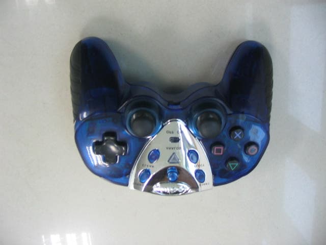
Click to zoom
Application Details
- Equipment Class
- DSS - Part 15 Spread Spectrum Transmitter
- Date of Grant
- Sep 15, 2005
- Application Purpose
- Original Equipment
- Date of Application
- Sep 15, 2005
- Equipment Note
- PS2 WIRELESS CONTROLLER : HOST
- Frequency Range
- 2402.15000000 - 2479.52000000
- Company
- Intec Inc.
- Country
- United States
Documents & Files
Document Text
Text extracted from the exhibit documents filed with the FCC. Open a document above to read the original.
Users Manual
*** Caution *** This device complies with part 15 of the FCC Rules. Operation is subject to the following two conditions: (1) This device may not cause harmful interference, and (2) this device must accept any interference received, including interference that may cause undesired operation. Changes of modifications not expressly approved by the party responsible for compliance could void the user’s authority to operate the equipment
Block Diagram
11 22 33 44 D D C C B B A A Ti tl e Nu mb er Revi sio n Size A4 Date: 2005-7-13 Sheet of Fil e: D: \mywo rk\ ..\D evice Bl ock D iag ram V 14. SCH DOC Drawn By: Wreless gmaepad device Ver 1.4 Functiom Block Diagram RF Module Battary MOTOR Main Control Chip BUTTON/AXIS LED OSC 13.824MHZ Tolerance:10ppm Step-Up DC/DC Converter VCC GND OSC INPUT PIN OUTPUT PIN OSC DIGITALBASEBANDINTERFACE DIGITALBASEBANDINTERFACE ANT INTERFACE VCC VCC GND GND 2400MHz 11 22 33 44 55 66 77 88 D D C C B B A A Ti tle Nu mb er Revis io n Size A3 Date: 2005-7-13 Sheet of Fil e: D: \mywork \..\PS2 Ho st Bl ock D iagram V1 3.SCHD OC Drawn By: PS2 wireless gmaepad Host Ver 1.4 PS2 INTERFACE Chip PS2 Console Functiom Block Diagram RF Module Main Control Chip CONNECT BUTTON LED OSC 13.824MHZ Tolerance:10ppm OSC INPUT PIN OUTPUT PIN OSC DIGITALBASEBANDINTERFACE DIGITALBASEBANDINTERFACE ANT INTERFACE VCC VCC GND GND 2400MHz OSC 16.000MHZ Tolerance:30ppm OSC Controller port Controller port VCC GND VCC GND DataExchangeInterface DataExchangeInterface
External Photos
Top View of Game Pad Bottom View of Game Pad Front View of Game Pad Back View of Game Pad Left View of Game Pad Right View of Game Pad Top View of Host Bottom View of Host Front View of Host Back View of Host Left View of Host Right View of Host
ID Label/Location Info
Model Name: G7089 Made in China FCC ID: RDDCYG70899192H
ID Label/Location Info
Model Name: G7089 Made in China FCC ID: RDDCYG70899192H
Internal Photos
Internal of Game Pad-1 Internal of Game Pad-2 Internal of Game Pad-3 Internal of Host-1 Internal of Host-2 Internal of Host-3
Operational Description
2.4GHz RF PS2 Wireless Controller Device Working Principle 1. It is a 2.4G RF product. It works at the frequency of ISM Band (2.4GHZ). There are up to 91 channels, and the frequency interval between each channel is 864K Hz. 2. Evenly Randomized Frequency Hopping Sequence method is implemented in the RF technology. 3. It works in “Slave” Mode. We call it “Device. The working procedures are: a) When power on, the Device will search all of the channels, to see whether there is a Host. b) If there is a Host, the Device will identity by the data received, to see whether it can be connected with the Host. c) If it can connect to the Host, then the Device will respond to the Host. d) The Host builds up the connection after receiving the response from the Device. e) The Host sends the command request to the Device for getting the Axes and Buttons value. f) The Device sends Axes and Button value to the Host. g) The Host identifies the data received and does the error detection and the error correction. h) The Host sends Motor commands to the Device. i) The Device will handle the Motor behaviors by the Motor data value that sent from the Host. j) Repeat from step e) to step i). Typical Product Characteristics: Items Description Type of Modulation GFSK Number of Channels 91 Frequency Band 2402 MHz ~ 2479 MHz Antenna Type PCB Antenna Testing Duty Cycle 100% Test Power Source DC 3V From battery Temperature Range(Operating) 0 ~ 50 Basic Function: - Fully compatible with PS2 Platform - Low power Indicator - Power on/off selection - Rubber grips - Auto Player matching - 10 Meter(30ft) 2.4G RF wireless transmitting & receiving distance 2.4GHz RF PS2 Wireless Controller Host Working Principle 4. It is a 2.4G RF product. It works at the frequency of ISM Band (2.4GHZ). There are up to 91 channels, and the frequency interval between each channel is 864K Hz. 5. Evenly Randomized Frequency Hopping Sequence method is implemented in the RF technology. 6. It works in “Master” Mode. We call it “Host.” The working procedures are: k) When power on, the Host will do the frequency hopping according to a certain sequence, and then send the connection command. l) If there is a Device response, the Host will judge whether it can be permitted to connect. m) If it can be permitted to connect, then send the connection command to build up the connection. n) The Host sends the request command to the Device to get the Axes and Buttons value. o) The Device sends the Axes and Buttons value to the Host. p) The Host will identify the data received and then do the data detection and data correction. q) The Host will save the data received if there is no error. r) The Host judges whether it is required to send Axes and Buttons value to PS2 console. s) If it is required, then send the saved data to PS2 console. t) The Host judges whether there is any Motor command and/or Motor value sent from PS2 console. u) If there is, then the Host will save the received Motor data. v) The Host send Motor commands to the Device, and send the Motor value to the Device. w) Repeat Step e) to Step l) x) Typical Product Characteristics: Items Description Type of Modulation GFSK Number of Channels 91 Frequency Band 2402 MHz ~ 2479 MHz Antenna Type PCB Antenna Testing Duty Cycle 100% Test Power Source DC 3.5V From PS2 Temperature Range(Operating) 0 ~ 50 Basic Function: - A LED Indicate Link & Search Mode Randomized Frequency Hopping Sequence Working Principle The sequence of the jump frequency will be settle by the host. The method is the host to be connected to the device,The sequence data S(8bit) and HostID(16bit) will bring through scan the RSSI of RF Module in different channel, and the data will be transmitted to the device. Then the both side will calculate to the next number (F) by same agument(S). The way of bring sequence is as follows: N: the numbers of useful channel S: number of seed (8bit)=S7-S0 P: replacement control (21bit)=P20-P0 ,Each 3 bit become one figure, as follow : Q6=P20P19P18 Q5=P17P16P15 Q4=P14P13P12 Q3=P11P10P9 Q2=P8P7P6 Q1=P5P4P3 Q0=P2P1P0 Qi≠Qj (0≤i<6, i<j≤6) to be request! F: the figure of the sequence (0≤F<N) Surpose the S to be S(k) in K cycle. It means the channel of the (K+1) cycle will be F(K+1) channel. 1. S(k+1)=S(k)+1=S(k+1)7~S(k+1)0 2. S(k+1)’s Bit6~Bit0 will conversion to R(k+1)=r(k+1)7~r(k+1)0 r(k+1)i= S(k+1)Qi (0≤i<6) , r(k+1)7 = s(k+1)7 to be request! 3. F(k+1)=R(k+1) mod N So we got to know from above procedure, S data is come from the device ,then transmitter the data to the device. And the above replace control data P is calculate from 16bit HostID of host by the Host and Device both side. Please reference to the following C program for to calculate method. void FindFHSeed(unsigned char HostIDH, unsigned char HostIDL) { //------------------------------------------------------------------------------ // The following code does the same job, but in C language format unsigned short b = 5040; unsigned short m; char i,j,k,l; m = (unsigned short)(HostIDH) *0x0100 + (unsigned short)(HostIDL); for (i=7; i>1; i--) { m %= b; b /= (unsigned short)i; q[i-1] = (unsigned char)(m / b); } q[0] = 0; for (i=6; i>0; i--) { for (j=i-1; j>=0; j--) { if (q[j] >= q[i]) q[j]++; do { l = 0; for (k=i; k<7; k++) { if (q[j] == q[k]) { q[j]++; l = 1; } } }while (l!=0); } } //------------------------------------------------------------------------- } void NextFrequencyHop() //Calculate the frequency channel of the next hop { //"seed" and "q[0]- q[6]" are known parameters. seed++; //Result is in r18 r11 = 0x01; if (seed & 0x80) r18 = 0x80; else r18 = 0x00; for (r10=0; r10<7; r10++) { if (r11 & seed) { r12 = q[r10]; r18 |= errorPattern[r12]; } r11 <<= 1; } while (r18 >= TOTAL_CHANNEL_NO) r18 -= TOTAL_CHANNEL_NO; }
Schematics
11 22 33 44 55 66 77 88 D D C C B B A A Ti tle Nu mb er Revis io n Size A3 Date: 2005-7-14 Sheet of File: D:\mywork\..\Intec_RF_Gamepad(Clear)_Device(AT)_Ver1[1]. 4.sch Drawn By: Intec_RF_Gamepad(Clear)_Device(AT) Ver1.4 1 / 1 RL.SU 80 50Q1 +3.3V 1KR1 80 50Q2 1KR2 2KR4 33 /0 .5WR622 /0 .5WR7 1N 41 48 D1 1N 41 48 D2 12 Smal l Mot or(Rig ht)J1 12 Big Motor(Left)J2 0. 1uF C1 0. 1uF C2 Vp p 82 3(5 %)-My larC3 Select/back SW1 Mode SW2 Star t SW3 CS 1 CLK 2 DI 3 DO 4 GN D 5 ORG 6 NU 7 VCC 8 93 LC46 /5 6 U1 +3.3V 10 KR8 Turbo SW4 10 KR9 2K R5 10 KR10 10 4 C4 AD L3 LXLY RXRY L_MAC L_ANA R3 AD Macro D5 AN A/ Pow erD6 10 4 C5 BT1 + 10 0u F C10 13 .82 4M X1 15 pF C11* 15 pF C12 1 2 3 4 5 6 7 8 Left_ st ickJ3 1 2 3 4 5 6 7 8 Right_StickJ4 Macro SW5 AD 1 2 3 4 5 6 7 8 Left_ st ick JP1 L3 /ltSW6 10 K LY 10 K LX 1 2 3 4 5 6 7 8 Right_stick JP2 R3/rtSW7 10 K RY 10 K RX Force Connect SW9 10 K R3 36 0k R15 10 0k R16 1N 58 17 D7 10 0U HL1 1N 41 48 D3 10 4C6 + 47 uF C16 +3.3V 10 KR11 SO 10 K LE FT 10 K UP 10 K RIGHT 10 K DO WN 10 K CRO/A/A 10 KSQU/X/B 10 KTRI/Y /Y 10 K CIR/B/X AD AD 10 K R1_key 10 K R2_key/Black/Z 10 K L 2_ key /W hi te/ Z 10 K L1 _key Os c_rf 10 4 C8 + 47 uF C17 Vo ut 3 Vi n 2 GN D 1 AIC1734-35 U4 Vo ut 2 SW 3 GN D 1 AIC16 42 -33/ LC36 1C U5 15 pFC13 10 KR12 10 K R13 10 K R14 Notice:(1)the components that marked "*" are not used temp orary 56 K R19 56 K R20 56 K R21 +3.3V 41424344 123478 1113141516 1819202122232425262728293031323334383940 569 1012 1737 3536 58 51 M0 04 0A A-D(MSK), 5 451 O0 40A AQ 044 -F(O TP PKG ) U2 Update History 10 4C19 Os c_bdTX DAT A SPICLK(Sclk)SPILTCH(Si)RXDATA(Dio) SPIDAT A(CSn) 10 4 C7 123456789 1011 RF ModuleCN4 SO TX DAT A SPILTCH(Si) SPICLK(Sclk) SPIDATA(CSn) RXDATA(Dio) BufferOn PC1 PC0 PLATFORM PS2 GCXBOX NO YES NO YES PC NONO YES YES VID SELECT NO Ucomm VC0 Ven dor ID PC2 NO ALL NONO NO NO NO YES 56 1PC0 56 1PC1 56 1PC2 56 1VC0 EN A3W EN A3W SPILTCH(Si) 18 R R17 Intec Stardard(Clear) VRF_SE LECT1S2 B1 B2 VRF_Select0 S1 + 10 uF C9 (2)Refer the following table: 2KR23 Mode D8 2KR24 Power Led D9 2KR25 Link Led D1 0 POWER_SW S3 Clear SW8 10 KR22 Optional Optional 3. 9K R26 No ti ce:R26 be used, has sleep function else no sleep function +3.3V 10 4 C14 2N 39 04Q3 15 0kR27 1kR28 BufferOn Os c_rf Os c_bd Vp p BATT 3V 4. 5V 6V the components in dashed line S1 S2 R17 C9 ONOp en Op en No us e On to B1On to B2 0R 0R 18 R NO NO 10 uF No us ed Must be usedNo us ed U4 Mus e be us ed: if MCU i s u se of EMP7 8P4 51, U4 :17 34 -35 MCU is us e of FM8P5 1, U 4:BL 850 3-25 Mus e be us ed: if MCU i s u se of EMP7 8P4 51, U4 :17 34 -35 MCU is us e of FM8P5 1, U 4:BL 850 3-25 Mus e be us ed: if MCU i s u se of EMP7 8P4 51, U4 :17 34 -35 MCU is us e of FM8P5 1, U 4:BL 850 3-35 Lo w po wer i ndi cat io n 2. 0V2. 0V 3. 7V3. 4V 4. 0V 4. 0V 56 0K R29 56 KR30 Platform: PS2/Xbox/GC Note: R30 only use for PS2 Platfom Ve r1 .3 Ver1 .4 Q3 39 04 NO Yes 11 22 33 44 D D C C B B A A Ti tl e Nu mb er Revi sio n Size A4 Date: 2005-7-14 Sheet of File: D:\mywork\..\Intec_PS2_RF_Host_AT_Ver1[1]. 5C(Intec).sch Drawn By: 16 MHz X1 15 pFC1 15 pFC2 VCC Tx DRxDSCKDT RDSR 1K R1 123456789 CON9J1 CLOCKCSD0D1D2D3D4D5D6D7 VCC Force Connect D1 10 4C6 VCC ACK FC(Force Connect) SW1 13 .82 4M X2 15 pF/? C3 15 pF/? C4 + 10 uF C11 1K R2 Di g_ st ick SW2 PSX/2 SW3* Neg _sel SW5 SO 35719264 DSRSCKDT R+3.3VGN D+8VRxDTx D +8V +8V 10 4C8 + 10 uF C7 Connect to J1 Ho st _No 0 SW6* Ho st _No 1SW7* 15 pFC5 Reserve SW18 Reserve SW17 Notice:the co mponents that marked "*" are not used tempo rary Ver1.5 1/ 1Al ex Intec_PS2_RF_Host_AT 10 4C13 10 4C14 Vo ut 3 Vi n 2 GN D 1 AIC1734-35U4 Led Flash SW19 Reserve SW20 ID0 ID3 ID1ID2 41424344 123478 1113141516 1819202122232425262728293031323334383940 569 1012 1737 3536 5201/5451M005AC-D(DICE) U1 414243441234781113141516 1819202122232425262728293031323334383940 5691012 1737 3536 54 51 M0 35 AA-D(D ice) U2 56 k R5 56 k R6 56 k R7 Os c_rf VCC TX DAT A SPICLK(Sclk)SPILTCH(Si)RXDA TA(D io) RSSI(Dclk) SPIDAT A(CSn ) Os c_bd EN A3W TX DAT ASPILTCH(Si)SPICLK(Sclk)RSSI(Dclk)SPIDATA(CSn)RXDA TA(D io)ID4ID5ID6ID7 VID _SEL2 SW14 VID _SEL1 SW13 VID _SEL3 SW15 VID _SEL4 SW16 CLOCKCSD0D1D2D3D4D5D6D7ACK 123456789 1011 RF Modu leCN4 SOEN A3W VCC 10 4 C16 2N 39 04Q1 15 0kR12 1kR13 Update History Ver1 .4 Ver1 .5 Q1 3904 NO Yes VID SELECT 110 1 ID7 ID6 ID5 ID4 Pin7 Pin8 Pin9 Pin10 Vendor ID A 1 11 1 B PS: 1 : Flo at 0: con net t o G ND Intec 0RR18 VCC
Test Report
Shenzhen Huatongwei International Inspection Co., Ltd REPORT NO: TR05070023 FCC ID: RDDCYG80899192H DATE: 09/08/2005 Page 1 Rev. 00 ELECTROMAGNETIC EMISSIONS COMPLIANCE REPORT INTENTIONAL RADIATOR CERTIFICATION TO FCC PART 15 SUBPART C REQUIREMENT OF XBOX WIRELESS CONTROLLER FCC ID: RDDCYG80899192H MODEL No.: G8089 BRAND NAME: N/A REPORT NO: TR05070023 ISSUE DATE: September 08, 2005 Prepared for INTEC INC. 5255 NW 159 TH STREET MIAMI, FL 33014 Prepared by SHENZHEN HUATONGWEI INTERNATIONAL INSPECTION CO., LTD d.b.a. SHENZHEN HUATONGWEI INTERNATIONAL INSPECTION CO., LTD HUATONGWEI BUILDING, KEJI RD. 12 S., HIGH-TECH PARK, NANSHAN DISTRICT, SHENZHEN, GUANGDONG , P.R.CHINA TEL: 86-755-26748099 FAX: 86-755-26748089 Shenzhen Huatongwei International Inspection Co., Ltd REPORT NO: TR05070023 FCC ID: RDDCYG80899192H DATE: 09/08/2005 Page 2 Rev. 00 VERIFICATION OF COMPLIANCE Applicant: INTEC INC. 5255 NW 159 TH STREET MIAMI, FL 33014 Manufacturer SHENZHEN CHUYAR ELECTRONICS CO., LTD BLDG 3, BAOZHOU IND. ESTATE 117 JIUWEI RD. BAO’AN, SHENZHEN Product Description: XBOX WIRELESS CONTROLLER Brand Name: N/A Model Number: G8092; G8089; G8091 Serial Number: N/A File Number: SQE05070023 Date of Test: July 25, 2005 ~ September 08, 2005 We hereby certify that: The above equipment was tested by SHENZHEN HUA TONG WEI INTERNATIONAL INSPECTION CO., LTD. The test data, data evaluation, test procedures, and equipment configurations shown in this report were made in accordance with the procedures given in ANSI C63.4 (2003) and the energy emitted by the sample EUT tested as described in this report is in compliance with radiated emission limits of FCC Rules Part 15.247. The test results of this report relate only to the tested sample identified in this report. Reviewed By Jimmy Li / Technical Manager SHENZHEN HUA TONG WEI INTERNATIONAL INSPECTION CO., LTD Shenzhen Huatongwei International Inspection Co., Ltd REPORT NO: TR05070023 FCC ID: RDDCYG80899192H DATE: 09/08/2005 Page 3 Rev. 00 Table of Contents 1. GENERAL INFORMATION................................................................................................3 1.1 Product Description..................................................................................................................4 1.2 Related Submittal(s) / Grant (s)................................................................................................4 1.3 Test Methodology.....................................................................................................................4 1.4 Test Facility..............................................................................................................................4 2. SYSTEM TEST CONFIGURATION..................................................................................5 2.1 Configuration of Tested System................................................................................................5 3. Summary of Test Result.........................................................................................................7 4. DESCRIPTION OF TEST MODES.....................................................................................7 5. PARAMETERS FOR GAME PAD......................................................................................8 5.1 Conduction Emission................................................................................................................8 5.2 Hopping Channels..................................................................................................................10 5.3 Channel Separation................................................................................................................12 5.4 20 dB Bandwidth....................................................................................................................13 5.5 Operation Frequency..............................................................................................................14 5.6 Peak Output Power.................................................................................................................15 5.7 Spurious Emission at Transmitting Mode...............................................................................18 5.8 Band Edge..............................................................................................................................21 5.9 Spurious Emission at Receiving Mode....................................................................................23 5.10 Dwell Time..............................................................................................................................25 6. PARAMETERS FOR HOST..............................................................................................26 6.1 Conduction Emission..............................................................................................................26 6.2 Hopping Channels..................................................................................................................27 6.3 Channel Separation................................................................................................................28 6.4 20 dB Bandwidth....................................................................................................................29 6.5 Operation Frequency..............................................................................................................30 6.6 Peak Output Power.................................................................................................................31 6.7 Spurious Emission at Transmitting Mode...............................................................................32 6.8 Band Edge..............................................................................................................................34 6.9 Spurious Emission at Receiving Mode....................................................................................36 6.10 Dwell Time..…
Text truncated - open the document above for the full version.
Test Report
Shenzhen Huatongwei International Inspection Co., Ltd REPORT NO: TR05070022 FCC ID: RDDCYG70899192H DATE: 09/05/2005 Page 1 Rev. 00 ELECTROMAGNETIC EMISSIONS COMPLIANCE REPORT INTENTIONAL RADIATOR CERTIFICATION TO FCC PART 15 SUBPART C REQUIREMENT OF PS2 WIRELESS CONTROLLER FCC ID: RDDCYG70899192H MODEL No.: G7089 BRAND NAME: N/A REPORT NO: TR05070022 ISSUE DATE: September 5, 2005 Prepared for INTEC INC. 5255 NW 159 TH STREET MIAMI, FL 33014 Prepared by SHENZHEN HUATONGWEI INTERNATIONAL INSPECTION CO., LTD d.b.a. SHENZHEN HUATONGWEI INTERNATIONAL INSPECTION CO., LTD HUATONGWEI BUILDING, KEJI RD. 12 S., HIGH-TECH PARK, NANSHAN DISTRICT, SHENZHEN, GUANGDONG , P.R.CHINA TEL: 86-755-26748099 FAX: 86-755-26748089 Shenzhen Huatongwei International Inspection Co., Ltd REPORT NO: TR05070022 FCC ID: RDDCYG70899192H DATE: 09/05/2005 Page 2 Rev. 00 VERIFICATION OF COMPLIANCE Applicant: INTEC INC. 5255 NW 159 TH STREET MIAMI, FL 33014 Manufacturer SHENZHEN CHUYAR ELECTRONICS CO., LTD BLDG 3, BAOZHOU IND. ESTATE 117 JIUWEI RD. BAO’AN, SHENZHEN Product Description: PS2 WIRELESS CONTROLLER Brand Name: N/A Model Number: G7092; G7089; G7091 Serial Number: N/A File Number: SQE05070022 Date of Test: July 25, 2005 ~ September 5, 2005 We hereby certify that: The above equipment was tested by SHENZHEN HUA TONG WEI INTERNATIONAL INSPECTION CO., LTD. The test data, data evaluation, test procedures, and equipment configurations shown in this report were made in accordance with the procedures given in ANSI C63.4 (2003) and the energy emitted by the sample EUT tested as described in this report is in compliance with radiated emission limits of FCC Rules Part 15.247. The test results of this report relate only to the tested sample identified in this report. Reviewed By Jimmy Li / Technical Manager SHENZHEN HUA TONG WEI INTERNATIONAL INSPECTION CO., LTD Shenzhen Huatongwei International Inspection Co., Ltd REPORT NO: TR05070022 FCC ID: RDDCYG70899192H DATE: 09/05/2005 Page 3 Rev. 00 Table of Contents 1. GENERAL INFORMATION................................................................................................4 1.1 Product Description..................................................................................................................4 1.2 Related Submittal(s) / Grant (s)................................................................................................4 1.3 Test Methodology.....................................................................................................................4 1.4 Test Facility..............................................................................................................................4 2. SYSTEM TEST CONFIGURATION..................................................................................5 2.1 Configuration of Tested System................................................................................................5 3. Summary of Test Result.........................................................................................................7 4. DESCRIPTION OF TEST MODES.....................................................................................7 5. PARAMETERS FOR GAME PAD......................................................................................8 5.1 Conduction Emission................................................................................................................8 5.2 Hopping Channels..................................................................................................................10 5.3 Channel Separation................................................................................................................12 5.4 20 dB Bandwidth....................................................................................................................13 5.5 Operation Frequency..............................................................................................................14 5.6 Peak Output Power.................................................................................................................15 5.7 Spurious Emission at Transmitting Mode...............................................................................18 5.8 Band Edge..............................................................................................................................20 5.9 Spurious Emission at Receiving Mode....................................................................................22 5.10 Dwell Time..............................................................................................................................24 6. PARAMETERS FOR HOST..............................................................................................25 6.1 Conduction Emission..............................................................................................................25 6.2 Hopping Channels..................................................................................................................26 6.3 Channel Separation................................................................................................................27 6.4 20 dB Bandwidth....................................................................................................................28 6.5 Operation Frequency..............................................................................................................29 6.6 Peak Output Power.................................................................................................................30 6.7 Spurious Emission at Transmitting Mode...............................................................................31 6.8 Band Edge..............................................................................................................................32 6.9 Spurious Emission at Receiving Mode....................................................................................34 6.10 Dwell Time......…
Text truncated - open the document above for the full version.
Test Setup Photos
Setup Photo-1 Setup Photo-2 Setup Photo-3 Setup Photo-4 Setup Photo-5
Contact Information
Applicant
YAMI PEREA(Manager)
Test Firm
Shenzhen Huatongwei International Insp. Co., LtdMoffy Yu
Technical Specifications
| # | Rule Parts | Frequency Range | Power Output |
|---|---|---|---|
| 1 | 15C | 2.40 GHz - 2.48 GHz | 11.00 mW |
Other Applications from Intec Inc.
RDDG7687
Sep 27, 20072.4GHz WIRELESS DEVICE
Equipment Class
DXX - Part 15 Low Power Communication Device Transmitter
RDDT10571-DRIVER
Dec 24, 2006Personal FM Broadcast Band Transmitter
Equipment Class
DXX - Part 15 Low Power Communication Device Transmitter
RDDT1055I-DRIVER
Oct 31, 2006IPOD FM Transmitter
Equipment Class
DXX - Part 15 Low Power Communication Device Transmitter
RDDTRANSMITTER
Feb 07, 2006Car Stereo Player
Equipment Class
DXX - Part 15 Low Power Communication Device TransmitterRDDCYG80899192H
Sep 19, 2005XBOX WIRELESS CONTROLLER-HOST
Equipment Class
DSS - Part 15 Spread Spectrum Transmitter