RDDWIRELESSJOYPADGame Cube Wireless Controller
Intec Inc.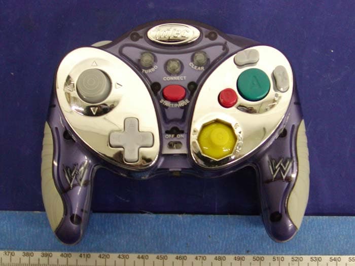
Click to zoom
Application Details
- Equipment Class
- DSS - Part 15 Spread Spectrum Transmitter
- Date of Grant
- Dec 29, 2004
- Application Purpose
- Original Equipment
- Date of Application
- Dec 29, 2004
- Equipment Note
- Game Cube Wireless Controller
- Frequency Range
- 2402.00000000 - 2481.00000000
- Company
- Intec Inc.
- Country
- United States
Documents & Files
Document Text
Text extracted from the exhibit documents filed with the FCC. Open a document above to read the original.
Block Diagram
11 22 33 44 D D C C B B A A Ti tl e Nu mb er Revi sio n Size A4 Date: 2004-12-3 Sheet of Fil e: C:\ Docu men ts and Set ti ngs \.. \DH _DE VICEv1 3.SCHD OC Drawn By: GAMECUBE wireless gmaepad device Ver 1.3 Functiom Block Diagram RF Module Battary MOTOR Main Control Chip BUTTON/AXIS LED OSC 16.000MHZ Tolerance:10ppm Step-Up DC/DC Converter VCC GND OSC INPUT PIN OUTPUT PIN OSC DIGITALBASEBANDINTERFACE DIGITALBASEBANDINTERFACE ANT BUFFER INTERFACE VCC VCC GND GND 2400MHz MIN:-18DBMMAX:-10DBM 11 22 33 44 55 66 77 88 D D C C B B A A Ti tle Nu mb er Revis io n Size A3 Dat e: 20 04 -12-3 Sheet of Fil e: C:\D ocu ment s an d Sett in gs\ ..\DH _H OSTV 13. SCH DOC Drawn By: GAMECUBE wireless gmaepad Host Ver 1.3 NGC INTERFACE Chip GAMECUBE Console Functiom Block Diagram RF Module Main Control Chip CONNECT BUTTON LED OSC 16.000MHZ Tolerance:10ppm OSC INPUT PIN OUTPUT PIN OSC DIGITALBASEBANDINTERFACE DIGITALBASEBANDINTERFACE ANT BUFFER INTERFACE VCC VCC GND GND 2400MHz MIN:-18DBMMAX:-10DBM OSC 16.000MHZ Tolerance:30ppm OSC Controller port Controller port VCC GND VCC GND DataExchangeInterface DataExchangeInterface
External Photos
EXHIBIT C - EUT EXTERNAL PHOTOGRAPHS Transmitter Front View Transmitter Rear View Transmitter Rear View with Battery Off Receiver Front View Receiver Rear View
ID Label/Location Info
EXHIBIT A - FCC ID LABEL INFORMATION Proposed FCC ID Label Specifications: Text is black or white in color and is left justified. Labels are silk- screened and shall be “permanently affixed” at a conspicuous location on the EUT. Proposed Label Location on EUT Bottom View of EUT /FCC ID Label FCC ID: RDDWIRELESSJOYPAD This device complies with Part 15 of the FCC Rules. Operation is subject to the following two conditions: (1) this device may not cause harmful interference, and (2) this device must accept any interference received, including interference that may cause undesired operation.
Internal Photos
EXHIBIT C - EUT INTERNAL PHOTOGRAPHS Transmitter Cover off View Transmitter Component View Transmitter Solder View Transmitter Small PCB Front Component View Transmitter Small PCB Rear Solder View Receiver Cover Off Top View Receiver Cover Off Right View Receiver Cover Off Left View Receiver Component View Receiver Solder View 1 Receiver Solder View 2
Operational Description
2.4GHz RF GAMECUBE Wireless Controller Host Working Principle 1. It is a 2.4G RF product. It works at the frequency of ISM Band (2.4GHZ). There are up to 80 channels, and the frequency interval between each channel is 1M Hz. 2. Evenly Randomized Frequency Hopping Sequence method is implemented in the RF technology. 3. It works in “Master” Mode. We call it “Host.” The working procedures are: a) When power on, the Host will do the frequency hopping according to a certain sequence, and then send the connection command. b) If there is a Device response, the Host will judge whether it can be permitted to connect. c) If it can be permitted to connect, then send the connection command to build up the connection. d) The Host sends the request command to the Device to get the Axes and Buttons value. e) The Device sends the Axes and Buttons value to the Host. f) The Host will identify the data received and then do the data detection and data correction. g) The Host will save the data received if there is no error. h) The Host judges whether it is required to send Axes and Buttons value to GAMECUBE console. i) If it is required, then send the saved data to GAMECUBE console. j) The Host judges whether there is any Motor command and/or Motor value sent from GAMECUBE console. k) If there is, then the Host will save the received Motor data. l) The Host send Motor commands to the Device, and send the Motor value to the Device. m) Repeat Step e) to Step l) 2.4GHz RF GAMECUBE Wireless Controller Device Working Principle 1. It is a 2.4G RF product. It works at the frequency of ISM Band (2.4GHZ). There are up to 80 channels, and the frequency interval between each channel is 1M Hz. 2. Evenly Randomized Frequency Hopping method is implemented in the RF technology. 3. It works in “Slave” Mode. We call it “Device.” The working procedures are: n) When power on, the Device will search all of the channels, to see whether there is a Host. o) If there is a Host, the Device will identity by the data received, to see whether it can be connected with the Host. p) If it can connect to the Host, then the Device will respond to the Host. q) The Host builds up the connection after receiving the response from the Device. r) The Host sends the command request to the Device for getting the Axes and Buttons value. s) The Device sends Axes and Button value to the Host. t) The Host identifies the data received and does the error detection and the error correction. u) The Host sends Motor commands to the Device. v) The Device will handle the Motor behaviors by the Motor data value that sent from the Host. w) Repeat from step e) to step i).
Operational Description
The sequence of the jump frequency will be settle by the host. The method is the host to be connected to the device , The sequence data S(8bit) and HostID(16bit) will bring through scan the RSSI of RF Module in different channel, and the data will be transmitted to the device. Then the both side will calculate to the next number (F) by same agument(S). The way of bring sequence is as follows: N: the numbers of useful channel S: number of seed (8bit)=S7-S0 P: replacement control (21bit)=P20-P0 ,Each 3 bit become one figure, as follow : Q 6 =P 20 P 19 P 18 Q 5 =P 17 P 16 P 15 Q 4 =P 14 P 13 P 12 Q 3 =P 11 P 10 P 9 Q 2 =P 8 P 7 P 6 Q 1 =P 5 P 4 P 3 Q 0 =P 2 P 1 P 0 Qi ≠ Qj (0 ≤ i<6, i<j ≤ 6) to be request! F: the figure of the sequence (0 ≤F<N) Surpose the S to be S(k) in K cycle. It means the channel of the (K+1) cycle will be F(K+1) channel. 1. S(k+1)=S(k)+1=S(k+1) 7~S(k+1)0 2. S(k+1) ’ s Bit6~Bit0 will conversion to R(k+1)=r(k+1) 7 ~r(k+1) 0 r(k+1) i = S(k+1) Qi (0≤i<6) , r(k+1) 7 = s(k+1) 7 to be request! 3. F(k+1)=R(k+1) mod N So we got to know from above procedure, S data is come from the device ,then transmitter the data to the device. And the above replace control data P is calculate from 16bit HostID of host by the Host and Device both side. Please reference to the following C program for to calculate method. void FindFHSeed(unsigned char HostIDH, unsigned char HostIDL) { //------------------------------------------------------------------------------ // The following code does the same job, but in C language format unsigned short b = 5040; unsigned short m; char i,j,k,l; m = (unsigned short)(HostIDH) *0x0100 + (unsigned short)(HostIDL); for (i=7; i>1; i--) { m %= b; b /= (unsigned short)i; q[i-1] = (unsigned char)(m / b); } q[0] = 0; for (i=6; i>0; i--) { for (j=i-1; j>=0; j--) { if (q[j] >= q[i]) q[j]++; do { l = 0; for (k=i; k<7; k++) { if (q[j] == q[k]) { q[j]++; l = 1; } } }while (l!=0); } } //------------------------------------------------------------------------- } void NextFrequencyHop() //Calculate the frequency channel of the next hop { //"seed" and "q[0]- q[6]" are known parameters. seed++; //Result is in r18 r11 = 0x01; if (seed & 0x80) r18 = 0x80; else r18 = 0x00; for (r10=0; r10<7; r10++) { if (r11 & seed) { r12 = q[r10]; r18 |= errorPattern[r12]; } r11 <<= 1; } while (r18 >= TOTAL_CHANNEL_NO) r18 -= TOTAL_CHANNEL_NO; }
Schematics
11 22 33 44 D D C C B B A A Ti tl e Nu mb er Revi sio n Size A4 Date: 2004-10-11 Sheet of File: F:\myfcc\CY-630RV11.SCH Drawn By: V1.1 10 MHz X1 15 pF C1 15 pF C2 VCC 1K R1 CLOCKCSD0D1D2D3D4D5D6D7 VCC Force Connect D1 10 4C13 VCC ACK FC(Force Connect) SW1 Bpk ctl_ rfBnd en_rf Bpk ctl_ bdBnd en_b dBnd en_b d 16 M X2 15 pF(*) C3 15 pF(*)C4 + 10 uF C11 1K R2 Bpk ctl_ bdBnpwr_bd BDdata + 10 uF C12 +5V +5V 10 4C8 + 10 uF C7 1 2 74 HC04U3 A 3 4 74 HC04U3 B 15 pFC5 BDclk_bdBDclk_bd 5 6 74 HC04U3 C 9 8 74 HC04U3 D BDclk_rf 10 4 C9 2. 5V 22 0 R3 1N 41 48 D2 2. 5V 1234567891011 RF_Mod uleRF1 Bpk ctl_ rfRxclkBnd en_rfOs c_rfBnpwr_rfBrclkBData1BDclk_rfBDdata +8V Os c_rf RxclkBrclkBData1 Bnpwr_rf Bnpwr_bd 11 10 74 HC04U3 E 41424344 123478 1113141516 1819202122232425262728293031323334383940 569 1012 1737 3536 SLA201U1 414243441234781113141516 1819202122232425262728293031323334383940 5691012 1737 3536 54 51 O00 2AA Q0 44-F(QFP)/5 20 1M007 AA -D (DICE) U2 10 4C14 10 4C14 XBOX _G C LK 0 LR_ SE LECT LK 1 12345 CON1 VCC NGC RF Host Electronic Sche matic Diag ram V1 .1 1/ 1 xf CYF63 01 101 11 22 33 44 55 66 77 88 D D C C B B A A Ti tle Nu mb er Revis io n Size A3 Date: 2004-10-11 Sheet of File: F:\myfcc\CY-630TV11.SCH Drawn By: V1.1 v1 .1 80 50Q1 3. 3V 1KR8 22 /0 .5WR5 12 Big Mo to r(Left)M1 0. 1uF C8 VMOT OR 82 3(5 %)-My larC15 Start S6 Tu rbo S3 10 KR15 2KR17 LXLY RXRY L_ ANA AD 10 uF C2 3VBT1 + 47 uF CE1 15 pF C12* 15 pF C11 Force Connect S7 10 KR24 24 0KR2568 0K R26 BData1 Bpkctl_bdBnd en_b dBDclk_bdBnpwr_bd 10 0U HL110 4C1 + 10 0u F CE2 +3.3V BDdata A B Y X AD AD Bpkctl_rfBnden_rf Bpkctl_bdBnden_bd 1 2 74 HC04U3 A BDclk_bd 3 4 74 HC04U3 B 5 6 74 HC04U3 C BDclk_rf 9 8 74 HC04U3 D Os c_bd Os c_bd Os co_rf 10 4 C14 2. 5V 1234567891011 RF_Mod uleRF1 Bpkctl_rfRxclkBnd en_rfOs co_rfBnpwr_rfBrclkBData1BDclk_rfBDdata + 10 uF CE4 22 0 R1 2. 5V 15 pFC13 10 KR12 10 KR11 10 KR10 RxclkBrclk BData1 Bnpwr_rf Bnpwr_bd 11 10 74 HC04 U3 E 56 K R20 56 K R21 56 K R22 56 K R23 +3.3V 41424344 123478 1113141516 1819202122232425262728293031323334383940 569 1012 1737 3536 54 51 O00 1A AQ0 44 -F(Q FP)/ 520 1M00 6A A-D(D ICE ) U1 10 4C10 VCC 14 GN D 7 13 12 74 HC04 U3 F 2KR3 2KR2 10 3C5 10 3C4 Clear S1 10 KR18 LY LX AD 1 2 3 POWERSW1 Vo ut 3 Vi n 2 GN D 1 AI C16 42 - 33 U5 1N 58 17D1 SCHOT TKY 1N 581 9D2 1N 41 48 D3 1N 41 48D4 Turbo Led LE D2 Power Led LE D4 Link Led LE D5 16 MX1 VMOT OR PLED PLED AD VBA T 2. 5V GN D +3.3V 132 6 4 5 0 3D_L 132 6 4 5 0 5MM3D-R RX RY L3 R3 AD LEFT DO WN UP RIGHT 1 2 3 4 5 CON2 12345 CON2A VBA T CLEAR TURLED TURBO START 1234567 CON1 1234567 CON1A UP LEFT RIGHT DO WN AD 1UP1LE FT 1RIGHT 1DO WN1 AD 1 UP1 LEFT1 RIGHT1 DO WN 1 CONNECT CONNECTCLEA RTU RL EDTU RBOSTARTLINK LEDGN DCON NECT1CLEA R1TU RL ED1TU RBO 1START1LINK LED 1GN D1 CONNECT1 CLEAR1 TURLED1 TURBO1 START1 L INK LE D1 LINKLED 10KVR2 10KVR1 Z Z1 Z 12 CON5A 12 CON5 12 CON3L L 12 CON4R R 12 CON3 L3GN D 12 CON4 R3GN D 10 RR27 3.3V SW3 P1 1N 40 01D6 2RR29 2KR30 RED 3LE D6 2KR4 1 1 2 2 3 3 4 4 5 5 6 6 SW DPDTSW2 3V 3V 22 0RR6 0R(**) R7 80 50 Q2 DZ 1 NGC RF Game Pad Electronic Schematic Diagram 1/ 1 xf CYF6301101
Test Report
Note: The test report is specially limited to the above company and the product model only. It may not be duplicated without prior written consent of Bay Area Compliance Laboratory Corporation. This report must not be used by the client to claim product certification, approval, or endorsement by NVLAP, NIST or any agency of the US Government. FCC 15.247 EMI MEASUREMENT AND TEST REPORT For INTEC INC. 5255 N.W.159 TH STREET MIAMI FLORIIDA 33014 FCC ID: RDDWIRELESSJOYPAD This Report Concerns: Original Report Equipment Type: Game Cube Wireless Controller Test Engineer: Snell Leong Report No.: R0409303 Test Date: 2004-11-12 Reviewed By: Ming Jin Prepared By: Bay Area Compliance Laboratory Corporation (BACL) 230 Commercial Street Sunnyvale, CA 94085 Tel: (408) 732-9162 Fax: (408) 732 9164 INTEC INC. FCC ID: RDDWIRELESSJOYPAD Report # R0409303Rpt-b.doc Page 2 of 35 FCC 15.247 Report TABLE OF CONTENTS INTEC INC. ..................................................................................................................................................................1 GENERAL INFORMATION.......................................................................................................................................4 PRODUCT DESCRIPTION FOR EQUIPMENT UNDER TEST (EUT) ....................................................................................4 OBJECTIVE...................................................................................................................................................................4 RELATED SUBMITTAL(S)/GRANT(S).............................................................................................................................4 TEST METHODOLOGY..................................................................................................................................................4 TEST FACILITY.............................................................................................................................................................4 SYSTEM TEST CONFIGURATION ..........................................................................................................................6 JUSTIFICATION.............................................................................................................................................................6 BLOCK DIAGRAM.........................................................................................................................................................6 EQUIPMENT MODIFICATIONS.......................................................................................................................................6 SUPPORT EQUIPMENT LIST AND DETAILS....................................................................................................................6 POWER SUPPLY INFORMATION.....................................................................................................................................6 CONFIGURATION OF TEST SYSTEM..............................................................................................................................7 TEST SETUP BLOCK DIAGRAM.....................................................................................................................................7 SUMMARY OF TEST RESULTS FOR FCC PART 15............................................................................................8 ANTENNA REQUIREMENT ......................................................................................................................................9 §15.207(A) - CONDUCTED EMISSION...................................................................................................................10 MEASUREMENT UNCERTAINTY..................................................................................................................................10 TEST SETUP................................................................................................................................................................10 SPECTRUM ANALYZER SETUP....................................................................................................................................10 TEST EQUIPMENT LIST AND DETAILS.........................................................................................................................10 TEST PROCEDURE......................................................................................................................................................10 ENVIRONMENTAL CONDITIONS..................................................................................................................................11 SUMMARY OF TEST RESULTS.....................................................................................................................................11 CONDUCTED EMISSIONS TEST DATA.........................................................................................................................11 PLOT OF CONDUCTED EMISSIONS TEST DATA...........................................................................................................11 §15.205 & §15.209 - RADIATED EMISSION...........................................................................................................14 MEASUREMENT UNCERTAINTY..................................................................................................................................14 TEST SETUP................................................................................................................................................................14 SPECTRUM ANALYZER SETUP....................................................................................................................................14 TEST EQUIPMENT LIST AND DETAILS.........................................................................................................................14 ENVIRONMENTAL CONDITIONS.......…
Text truncated - open the document above for the full version.
Test Setup Photos
EXHIBIT B - TEST SETUP PHOTOGRAPHS Conducted Emission Radiated Emission
Contact Information
Applicant
YAMI PEREA(Manager)
Test Firm
Bay Area Compliance LaboratoryJohn Chan
Technical Specifications
| # | Rule Parts | Frequency Range | Power Output |
|---|---|---|---|
| 1 | 15C | 2.40 GHz - 2.48 GHz | 129.00 µW |
Other Applications from Intec Inc.
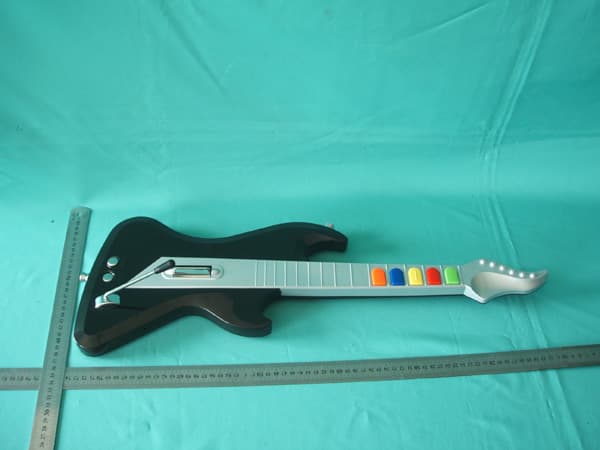
RDDG7687
Sep 27, 20072.4GHz WIRELESS DEVICE
Equipment Class
DXX - Part 15 Low Power Communication Device Transmitter
RDDT10571-DRIVER
Dec 24, 2006Personal FM Broadcast Band Transmitter
Equipment Class
DXX - Part 15 Low Power Communication Device Transmitter
RDDT1055I-DRIVER
Oct 31, 2006IPOD FM Transmitter
Equipment Class
DXX - Part 15 Low Power Communication Device Transmitter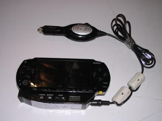
RDDTRANSMITTER
Feb 07, 2006Car Stereo Player
Equipment Class
DXX - Part 15 Low Power Communication Device TransmitterRDDCYG80899192H
Sep 19, 2005XBOX WIRELESS CONTROLLER-HOST
Equipment Class
DSS - Part 15 Spread Spectrum Transmitter