RZY00060VHF AVIONICS RADIO
Avidyne Corporation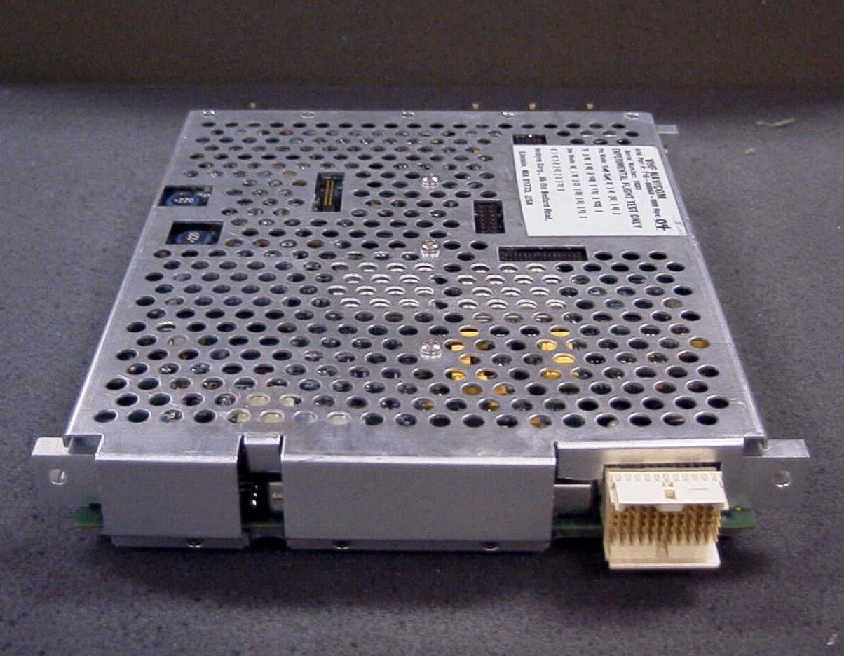
Click to zoom
Application Details
- Equipment Class
- TNB - Licensed Non-Broadcast Station Transmitter
- Date of Grant
- Oct 15, 2006
- Application Purpose
- Original Equipment
- Date of Application
- Oct 10, 2006
- Equipment Note
- VHF AVIONICS RADIO
- Frequency Range
- 118.00000000 - 136.99900000
- Company
- Avidyne Corporation
- Country
- United States
Documents & Files
Document Text
Text extracted from the exhibit documents filed with the FCC. Open a document above to read the original.
Users Manual
Avidyne DVX-740/750 VHF Nav/Com Module Installation & Initial Checkou t AVIDYNE CORPORATION 55 Old Bedford Road Lincoln, MA 01773 and 420 N. Wickham Rd, Suite B Melbourne, FL 32935 Document Number 610-00060-xxx Control Category CC2 Revision Description ECO Date 00 Release for FCC testing 6/15/2006 DCO-06-104 06/13/06 01 Revised per FCC Timco review 10/03/2006 DCO-06-211 10/09/06 Confidential property of Avidyne Corporation Not to be disclosed without permission DVX-740/750 VHF Nav/Com Installation & Checkout Manual Table of Contents 1. Scope and Purpose...............................................................3 2. Configuration of the DVX-750 Module.................................3 3. Specification of the DVX-750 Module..................................5 3.1 - FAA Certification Objectives............................................................................................7 TSO Applicability..............................................................................................................7 Environmental Category...................................................................................................8 Computer Software..........................................................................................................9 Hardware Assurance........................................................................................................9 3.2 - FCC Certification Objectives............................................................................................9 4. Circuit Description and Theory of Operation...................10 5. Initial Checkout and Test Procedure.................................17 6. Glossary...............................................................................21 Confidential property of Avidyne Corporation 610-00060- Not to be disclosed without permission Revision: -01 Date:10/09/2006 Page 2 of 21 DVX-740/750 VHF Nav/Com Installation & Checkout Manual 1. Scope and Purpose The purpose of this manual is to verify functionality of the DVX-750 VHF Nav/Com radio before installation into a host PFD chassis. End user operation of the DVX-750 is defined by the user I/O devices and displays that are provided by the host chassis. Therefore, this is not a “User’s Manual” for the end user (customer), but provides some direction for those who need to operate the DVX-750 module “stand-alone” during development, certification, production, or repair activities. 2. Configuration of the DVX-740/750 Module The DVX-750 top level module, Part# 710-00060-( ), consists of metal and mechanical parts as captured in the top level part as well as the following internal boards: a. RF Board, 320-00116-( ) b. DSP Board, 320-00115-( ) The DVX-740 is the same module but with the Marker Beacon receiver disabled on the RF Board. There are no changes to the Digital Board. The BNC connector for the Marker Beacon receiver is installed, so the external connection of the module thru the rear panel of the chassis is the same with either configuration. Fig 1.1 – DVX-740/750 VHF Nav/Com Module. Confidential property of Avidyne Corporation 610-00060- Not to be disclosed without permission Revision: -01 Date:10/09/2006 Page 3 of 21 DVX-740/750 VHF Nav/Com Installation & Checkout Manual The assembled DVX-750 slides into the host chassis, engaging the 60-pin backplane connector which provides power and ground connections as well as the Byteflight data interface for control (input) and data output. Installation steps are simply seating the unit in the cardguides and ensuring that the backplane connector is engaged, then tightening the Allen head retainer screws. After the rear panel is installed on the chassis the BNC retainer nuts with star washers must be installed. Figure 1.2 – DVX-750 Module installed in a Primary Flight Display (Chassis shown is Avidyne Part#, 700-00078-000). Confidential property of Avidyne Corporation 610-00060- Not to be disclosed without permission Revision: -01 Date:10/09/2006 Page 4 of 21 DVX-740/750 VHF Nav/Com Installation & Checkout Manual 3. Specification of the DVX-740/750 Module The DVX-750 VHF radio module operates as an airborne VHF COMM transceiver allowing a flight crew to aurally communicate with Air Traffic Control (ATC), other ground stations, or different aircraft in the VHF aeronautical band. It also operates as an airborne ILS/VOR receiver for radio aided navigation and guidance. The DVX-750 must be hosted by a PFD (Primary Flight Display) chassis, which provides conditioned DC power and digital interface to control radio functions. In ILS mode the VHF radio estimates own aircraft horizontal and vertical deviation from the selected ILS localizer and glide paths. In VOR mode it estimates own aircraft bearing to the selected VOR ground station relative to magnetic north (at the station). In addition, any speech or identification audio signals are presented aurally to the flight crew. The DVX-750 radio can also operate as an airborne Marker Beacon receiver and provides some Audio Panel functionality allowing it to interface to headsets (microphone and headphones), a cabin speaker and a transmitter key without requiring and audio panel. Table 3-1. VHF Radio Characteristics Summary Audio System 6 microphone or line in 5 headphone or line out 1 speaker out Headphone outputs: 35mW into 150 ohm <1% THD, 65mW into 150 ohm <10% THD Speaker output: 8W into 4 ohms -Frequency response: 300 to 6000Hz within 6dB Marker Beacon Receiver (optional) Operating frequency: 75MHz Selectivity: 6dB at least +10 kHz, 40dB no more than +200 kHz Sensitivity (high): 200uV (factory default) Glideslope Receiver Operating frequency: 328.60 to 335.40 MHz Channel # / spacing: 40 channels at 150 kHz spacing Selectivity: 6dB at least +21 kHz, 40dB no more than +160 kHz Sensitivity (flag): 36uV max Spurious response: -60dB or better Centering accuracy: 0 +0.02 DDM or better Defection response: 67% of final value in 600msec Localizer Rcvr Operating frequenc…
Text truncated - open the document above for the full version.
Block Diagram
12V RF/Digital Stacking Connector H G F E D C B A 87654321 H G F E D C B A 87654321 CONFIDENTIAL PROPERTY OF AVIDYNE CORPORATION. DO NOT REPRODUCE OR DISCLOSE WITHOUT EXPRESS PERMISSION. DRAWN: Sami Wahab CHECKED: Mark Haines VHF COM_NAV RADIO ARCHITECTURE DIAGRAM AVIDYNE CORPORATION 420 N. Wickham Road Suite B Melbourne, FL 32935 SIZEFSCM NODWG NOREV CXXX-XXXXX-XXXA SCALE 1 : 1 SHEET 1 OF 1 REV.DESCRIPTIONDATEBY FPGA LOC / VOR Rcvr DUC Glide Slope Rcvr Markr Beacn Rcvr VHF COMM Rcvr VHF COMM Transmitter VCO PLL Synth 57M VCXO 49M VCXO 20M TCXO FLASH SRAM T/ R COM Ant MB Ant G/S Ant NAV Ant Audio CODEC 1 Audio CODEC 2 Audio CODEC 3 9S12 Data Bus Processor SRAM Audio Interface Auxiliary Digital Signal Processor EEPROMEEPROM CPLD RS485 Transceiver RS232 Transceiver SRAM Discrete Input Register Discrete Interface lock_det iq_mod(14) tr_en pdclk nav_ch1 I2C SPI SPI Addr / Data nav_ch2 nav_ch3 nav_ch4 com_ch1 com_ch2 com_ch3 com_ch4 spi_tune aud1_in aud1_out aud2_in aud2_out aud3_in aud3_out aud_mclk disc_out Addr / Data cic_ovfl dsp1_reset_n dsp1_int dsp1_ardy GPIO TXCLK_ENABLE CODEC1_CSn CODEC2_CSn CODEC3_CSn APA_MUTEn DUC_RESETn DDCC_RESETn DDCN_RESETn dsp2_reset_n dsp2_int dsp2_ardy rs232_rx rs232_tx A/D NAV DDC 4 chan A/D NV_ATTEN GS_ATTEN A/D A/D CM_ATTEN COMM DDC 4 chan RS232 Transceiver Audio Connector SPEAKER HP_LINE_1 HP_LINE_2 HP_LINE_3 HP_LINE_4 HP_LINE_5 MIC_LINE_1 MIC_LINE_2 MIC_LINE_3 MIC_LINE_4 MIC_LINE_5 MIC_LINE_6 TX_KEY_1 TX_KEY_2 TX_KEY_3 DSCR_IN_1 DSCR_IN_2 DSCR_IN_3 DSCR_IN_4 RS232_BF RS232_FPGA DSCR_OUT_1 DSCR_OUT_2 Voltage Monitor Interface tr_switch pa_pwr pa_en pa_mon 12V_MON 10V_MON 5V_MON 3.3V_MON 2.5V_MON 1.6V_MON DIGITAL_TEMP ANLG_IN_0 ANLG_IN_1 ANLG_IN_2 ANLG_IN_4 HC912_VREF PA_MON PA_PWR TR_SWITCH PA_EN LOAD_SHED_Bn CH_IN_2 CH_IN_1 CH_IN_0 SLT_IN_4 SLT_IN_3 SLT_IN_2 SLT_IN_1 SLT_IN_0 BF_DATABUS 28V_MON 26V_MON RF_TEMP bf_sys_reset_n RF Connector Digital Card Voltage Monitors FPSM Connector Byteflight Data Bus Controller SPI THIS DOCUMENT NOT INTENDED FOR SYSTEM/AIRFRAME INSTALLATION PURPOSES Cypress Clock PLL bf_clk_pull 40M 10M Clock bf_eclk Addr / Data flash_page VCXO Trim DAC Primary Digital Signal Processor to NAV A/D, DDC to COMM A/D, DDC clk_49m clk_57m clk_ref 49M 57M I2C 20M TCXO 196M XO PA_Enable TR_Enable RF Board FPSM Connector +28V 5V 3.3V 7V 23V 3.3V SwitcherLinear 5V_DIG 12V_DIG 3.3V_DIG 2.5V 1.6V Prepared for Users Manual --6/15/06DMH 10V 5V 5V 5V 5V OV/UV Protect
Cover Letter(s)
10/9/06 420 N. Wickham Rd Melbourne, FL 32935 Tel: (321) 751-8400 Fax: -8435 From: D. Mark Haines 9 October 2006 To: Federal Communications Commission Authorization and Evaluation Division Subject: Confidentiality Request regarding application for certification of FCC ID: RZY00060 Pursuant to Sections 0.457 and 0.459 of the Commission’s Rules, we hereby request confidential treatment of information accompanying this application as outlined below: 1. Schematics of Unit: (PDF files: 330-00115-000 and 330-00116-000) 2. Parts List (710-00060-000_DVX750_BOM_Rev01.txt) 3. Tune-up Procedure (630-00647-000 RF Module Test and Alignment Procedure.doc) The above materials contain trade secrets and proprietary information not customarily released to the public. The public disclosure of these materials may be harmful to the applicant and provide unjustified benefits to its competitors. The applicant understands that pursuant to Section 0.457 of the Rules, disclosure of this application and all accompanying documentation will not be made before the date of the Grant for this application. Sincerely, D. Mark Haines Principal RF Engineer Attached: Copy of FCC Confidentiality Policy cc: Timco Engineering Inc. 849 N.W. State Road 45 P.O. Box 370 Newberry, FL 32669
External Photos
Applicant: Avidyne External Photos
ID Label/Location Info
FCC ID Label
ID Label/Location Info
Proposed FCC ID Label Location
Internal Photos
Applicant: Avidyne Internal Photos
Operational Description
DVX-740/750 VHF Nav/Com Circuit Description Error! Reference source not found. Error! Reference source not found. Error! Reference source not found. Revision: -00 Date:6/13/2006 Page 1 of 9 Circuit Description and Theory of Operation NOTE: Refer to Block Diagram (Fig 4.1) and circuit schematics during the following description. The DVX-750 VHF radio module operates as an airborne VHF COMM transceiver allowing a flight crew to aurally communicate with Air Traffic Control (ATC), other ground stations, or different aircraft in the VHF aeronautical band. It also operates as an airborne ILS/VOR receiver for radio aided navigation and guidance. The DVX-750 must be hosted by a PFD (Primary Flight Display) chassis, which provides conditioned DC power and digital interface to control radio functions. The DVX-750 consists of two internal printed circuit boards, the “RF Board” (Part# 310-00116-00x) and the “Digital Board” (Part# 310-00115-00x). The concept is to for analog signal processing to occur on the RF board and digital processing to be performed on the Digital Board. The choice was made to do the analog-to-digital conversions on the Digital board with carefully matched analog differential signals interfacing between the two boards thru a 50- mil pitch stacking connector. The transmitted signal is generated digitally and converted to analog on the Digital board and sent to the RF board, while the received signals, which represent the entire operational radio band for each receiver, are fed into the Digital board as differential analog signals and immediately converted to digital format to be channelized and demodulated by the digital downconverter and signal processor. While there can only be one transmitted signal at a time, there can be as many as eight receivers operating simultaneously. Note that nothing changes on the RF board when a receiver frequency is changed, since the entire radio band is fed into the Digital board. The receivers are identified as: Nav Rcvr – Tuned to condition and pass only the 108Mhz to 118Mhz Localizer and VOR Navigation bands such that the digitizer on the Digital board can undersample the RF signal without Nyquist alias signals appearing from out-of-band interference. The analog circuitry on the RF board provides the necessary filtering of signals that would appear in the Nyquist bands, and it applies the gain needed to optimize sensitivity based on signal strength of the in-band signals.. Glideslope Rcvr – Tuned to pass the 326 to 335 Mhz Glideslope signal band, it also provides sufficient filtering to allow the digitizer to undersample the received RF without causing Nyquist alias responses from out-of-band interference. Marker Beacon Rcvr – Very tightly tuned to pass only a single channel at 75Mhz, this receiver includes a custom crystal filter and also allows undersampling of the RF signal. Comm Rcvr – Tuned to pass only the 118 to 137Mhz VHF aeronautical band, this receiver interfaces to a T/R switch, allowing it to share the same antenna with the 16W DVX-740/750 VHF Nav/Com Circuit Description Error! Reference source not found. Error! Reference source not found. Error! Reference source not found. Revision: -00 Date:6/13/2006 Page 2 of 9 Comm transmitter. It also provides anti-aliasing filtering and optimizes gain for sensitivity without allowing signals to overload the A/D converters doing the DVX-740/750 VHF Nav/Com Circuit Description Error! Reference source not found. Error! Reference source not found. Error! Reference source not found. Revision: -00 Date:6/13/2006 Page 3 of 9 12V RFConnector FPGA LOC / VOR Rcvr DUC Glide Slope Rcvr Markr Beacn Rcvr VHF COMM Rcvr VHF COMM Transmitter VCO PLL Synth 57M VCXO 49M VCXO 20M TCXO FLASH SRAM T/R COM Ant MB Ant G/S Ant NAV Ant Audio CODEC 1 Audio CODEC 2 Audio CODEC 3 9S12 Data Bus Processor SRAM Audio Interface Auxiliary Digital Signal Processor EEPROM EEPROM CPLD RS485 Transceiver RS232 Transceiver SRAM Discrete Input Register Discrete Interface lock_det iq_mod(14)tr_enpdclk nav_ch1 I2C SPI SPI Addr / Data nav_ch2nav_ch3nav_ch4 com_ch1com_ch2com_ch3com_ch4 spi_tune aud1_inaud1_outaud2_inaud2_outaud3_inaud3_outaud_mclkdisc_out Addr / Data cic_ovfl dsp1_reset_n dsp1_int dsp1_ardy GPIO TXCLK_ENABLECODEC1_CSnCODEC2_CSnCODEC3_CSnAPA_MUTEnDUC_RESETnDDCC_RESETnDDCN_RESETn dsp2_reset_n dsp2_int dsp2_ardy rs232_rxrs232_tx A/D NAV DDC 4 chan A/D NV_ATTEN GS_ATTEN A/D A/D CM_ATTEN COMM DDC 4 chan RS232 Transceiver Audio Connector SPEAKER HP_LINE_1HP_LINE_2HP_LINE_3HP_LINE_4HP_LINE_5 MIC_LINE_1MIC_LINE_2MIC_LINE_3MIC_LINE_4MIC_LINE_5MIC_LINE_6 TX_KEY_1TX_KEY_2TX_KEY_3 DSCR_IN_1DSCR_IN_2DSCR_IN_3DSCR_IN_4 RS232_BF RS232_FPGA DSCR_OUT_1DSCR_OUT_2 Voltage Monitor Interface tr_switch pa_pwr pa_en pa_mon 12V_MON10V_MON5V_MON3.3V_MON2.5V_MON1.6V_MONDIGITAL_TEMPANLG_IN_0ANLG_IN_1ANLG_IN_2ANLG_IN_4HC912_VREFPA_MONPA_PWRTR_SWITCHPA_ENLOAD_SHED_Bn28V_MON26V_MONRF_TEMP bf_sys_reset_n RF Connector Digital Card Voltage Monitors FPSM Connector Byteflight Data Bus Controller SPI Cypress Clock PLL bf_clk_pull 40M 10M Clock bf_eclk Addr / Data flash_page VCXO Trim DAC Primary Digital Signal Processor to NAVA/D, DDCto COMMA/D, DDC clk_49m clk_57m clk_ref 49M57M I2C 20M TCXO 196M XO PA_EnableTR_Enable RF Board FPSM Connector +28V 5V 3.3V 7V 23V 3.3V Switcher Linear 5V_DIG 12V_DIG 3.3V_DIG 2.5V 1.6V 10V 5V 5V5V5V OV/UV Protect Figure 4.1 – VHF Nav/Com Block Diagram DVX-740/750 VHF Nav/Com Circuit Description Error! Reference source not found. Error! Reference source not found. Error! Reference source not found. Revision: -00 Date:6/13/2006 Page 4 of 9 Circuit Description by Functional Group (refer to the block diagram Figure 4.1): 1. Nav Receiver : The Nav Receiver connects to a VOR/Localizer antenna via BNC connector J1 at the rear of the DVX-750 module. For lightning protection the input signal is immediately bypassed by gas-discharge tube G1 if the voltage exceeds 90V peak. The desired radio signal or any remaining pulse from a lightn…
Text truncated - open the document above for the full version.
Test Report
FCC PART 87 TEST REPORT APPLICANT Avidyne Corporation 420 N Wickham Road Melbourne FL 32935 FCC ID RZY00060 MODEL NUMBER DVX-740/750 PRODUCT DESCRIPTION Aviation (Aircraft) Radio DATE SAMPLE RECEIVED June 12, 2006 DATE TESTED June 15 th , 2006 TESTED BY Joe Scoglio APPROVED BY Mario de Aranzeta TIMCO REPORT NO. A\AVIDYNE\1239AUT6\1239AUT6TestReport.doc TEST RESULTS PASS FAIL THE ATTACHED REPORT SHALL NOT BE REPRODUCED EXCEPT IN FULL WITHOUT THE WRITTEN APPROVAL OF TIMCO ENGINEERING, INC. 849 NW STATE ROAD 45 NEWBERRY, FL 32669 USA PH: 888.472.2424 OR 352.472.5500 FAX: 352.472.2030 EMAIL: [email protected] HTTP: //WWW.TIMCOENGR.COM Certificate # 0955-01 Applicant: Avidyne Corporation FCC ID: RZY00060 Report: A\AVIDYNE\1239AUT6\1239AUT6TestReport.doc Page 2 of 19 TABLE OF CONTENTS STATEMENT OF COMPLIANCE.................................................................................. 3 GENERAL INFORMATION .......................................................................................... 4 EMC EQUIPMENT LIST ............................................................................................. 6 TEST PROCEDURE ................................................................................................... 7 RF POWER OUTPUT .................................................................................................. 8 MODULATION CHARACTERISTICS............................................................................ 9 VOICE MODULATED COMMUNICATION EQUIPMENT ............................................. 10 FIELD STRENGTH OF SPURIOUS EMISSIONS......................................................... 16 FREQUENCY STABILITY.......................................................................................... 18 POWER LINE CONDUCTED INTERFERENCE........................................................... 19 Applicant: Avidyne Corporation FCC ID: RZY00060 Report: A\AVIDYNE\1239AUT6\1239AUT6TestReport.doc Page 3 of 19 STATEMENT OF COMPLIANCE Certificate # 0955-01 This equipment has been tested in accordance with the standards identified in the referenced test report. To the best of my knowledge and belief, these tests were performed using the measurement procedures described in this report and demonstrate that the equipment complies with the appropriate standards. No modifications were made to the equipment during testing in order to demonstrate compliance with these standards. I attest that the necessary measurements were made by me or under my supervision, at Timco Engineering, Inc. located at 849 N.W. State Road 45, Newberry, Florida 32669 USA. Authorized by: Mario de Aranzeta Signature: Function: Engineer Date: July 7 th , 2006 Tested by: Joe Scoglio Signature: on file Applicant: Avidyne Corporation FCC ID: RZY00060 Report: A\AVIDYNE\1239AUT6\1239AUT6TestReport.doc Page 4 of 19 GENERAL INFORMATION DUT Specification The test results relate only to the items tested. DUT Description AM Aviation Transciever (Aircraft) FCC ID RZY00060 Model Number DVX-740/750 Operating Frequency 118.000 to 136.992 MHz Type of Emission 6k0A3E Modulation AM 110–120Vac/50– 60Hz DC Power 28 Vdc DUT Power Source Battery Operated Exclusively Prototype Pre-Production Test Item Production Fixed Mobile Type of Equipment Portable Antenna N/A Antenna Connector BNC Applicant: Avidyne Corporation FCC ID: RZY00060 Report: A\AVIDYNE\1239AUT6\1239AUT6TestReport.doc Page 5 of 19 Test Facility: The test sites used by Timco Engineering Inc. for collecting radiated and conducted emission data is located at 849 NW State Road 45 Newberry, FL 32669 USA. Test Condition: The DUT was tested in the laboratory in an environment with normal temperature and humidity. The temperature was 26ºC with a relative humidity of 50%. Modification to the DUT: No modification was made to the DUT during testing. Test Exercise (e.g software description, test signal, etc.): The DUT was placed in continuous transmit mode of operation. Applicable Standards: TIA 603-C-2004 FCC CFR 47 Part 87 Part 2.1033(c) (4) Type of Emission: 6K0A3E Bn = 2M M = 3000 Bn = 2(3000) = 6k The authorized bandwidth is 25 kHz. Part 2.1033(c)(8) DC Voltages and Current into Final Amplifier: POWER INPUT: FINAL AMPLIFIER ONLY INPUT POWER – HIGH: (28 Vdc)(3.0A) = 84 Watts Applicant: Avidyne Corporation FCC ID: RZY00060 Report: A\AVIDYNE\1239AUT6\1239AUT6TestReport.doc Page 6 of 19 EMC EQUIPMENT LIST Device Manufacturer Model Serial Number Cal/Char Date Due Date Analyzer Tan Tower Spectrum Analyzer HP 8566B Opt 462 3138A07786 3144A20661 CAL 12/7/05 12/7/07 Analyzer Tan Tower RF Preselector HP 85685A 3221A01400 CAL 12/7/05 12/7/07 Analyzer Tan Tower Quasi-Peak Adapter HP 85650A 3303A01690 CAL 12/8/05 12/8/07 Analyzer Tan Tower Preamplifier HP 8449B-H02 3008A00372 CAL 12/8/05 12/8/07 Antenna: Biconnical Electro- Metrics BIA-25 1171 CAL 4/29/05 4/29/07 Antenna: Log-Periodic Electro- Metrics LPA-25 1122 CAL 8/26/04 8/26/06 Antenna: Double- Ridged Horn Electro- Metrics RGA-180 2319 CAL 12/29/04 12/29/06 LISN Electro- Metrics ANS-25/2 2604 CAL 8/27/04 8/27/06 Termaline Wattmeter Bird Electronic Corporation 611 16405 CAL 7/16/04 7/16/06 Applicant: Avidyne Corporation FCC ID: RZY00060 Report: A\AVIDYNE\1239AUT6\1239AUT6TestReport.doc Page 7 of 19 TEST PROCEDURE Power Line Conducted Interference: The procedure used was ANSI 63.4 2003 using a 50uH LISN. Both lines were observed with the UUT transmitting. The bandwidth of the spectrum analyzer was 10 kHz with an appropriate sweep speed. Power Output: The RF power output was measured at the antenna feed point using a power meter. Antenna Conducted Emissions: The RBW = 100 kHz, VBW = 300 kHz and the span set to 10.0 MHz and the spectrum was scanned from 30 MHz to the 10 th Harmonic of the fundamental. Radiation Interference: The test procedure used was ANSI/TIA 603 using an Agilent spectrum receiver with pre-selector. The bandwidth (RBW) of the spectrum receiver was 100 kHz up to 1 GHz and 1 MHz above 1 GHz using an approp…
Text truncated - open the document above for the full version.
Contact Information
Applicant
Roger E Mitchell(Sr. V.P. of Operations)
Test Firm
Timco Engineering, Inc.Sid Sanders
Technical Specifications
| # | Rule Parts | Frequency Range | Power Output | Emission | Tolerance |
|---|---|---|---|---|---|
| 1 | 87 | 118 MHz - 136.999 MHz | 16 W | 6K0A3E | 0.5000000000 ppm |
Other Applications from Avidyne Corporation
RZYIFDXXXV
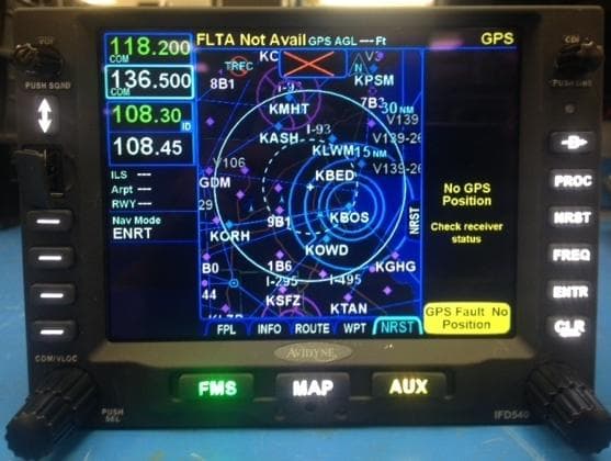
May 05, 2014VHF NAV/COM RADIO WITH WIFI AND BT
Equipment Class
TNB - Licensed Non-Broadcast Station Transmitter
RZYTAS6XX-A
Jul 25, 2013TRANSPONDER
Equipment Class
TNB - Licensed Non-Broadcast Station Transmitter
RZYMLB7XX
Jul 09, 2007Remote control for a Multilink Broadcast Receiver
Equipment Class
DXX - Part 15 Low Power Communication Device Transmitter