SKA13192-SARDDTS Transceiver
Freescale Semiconductor Danmark A/S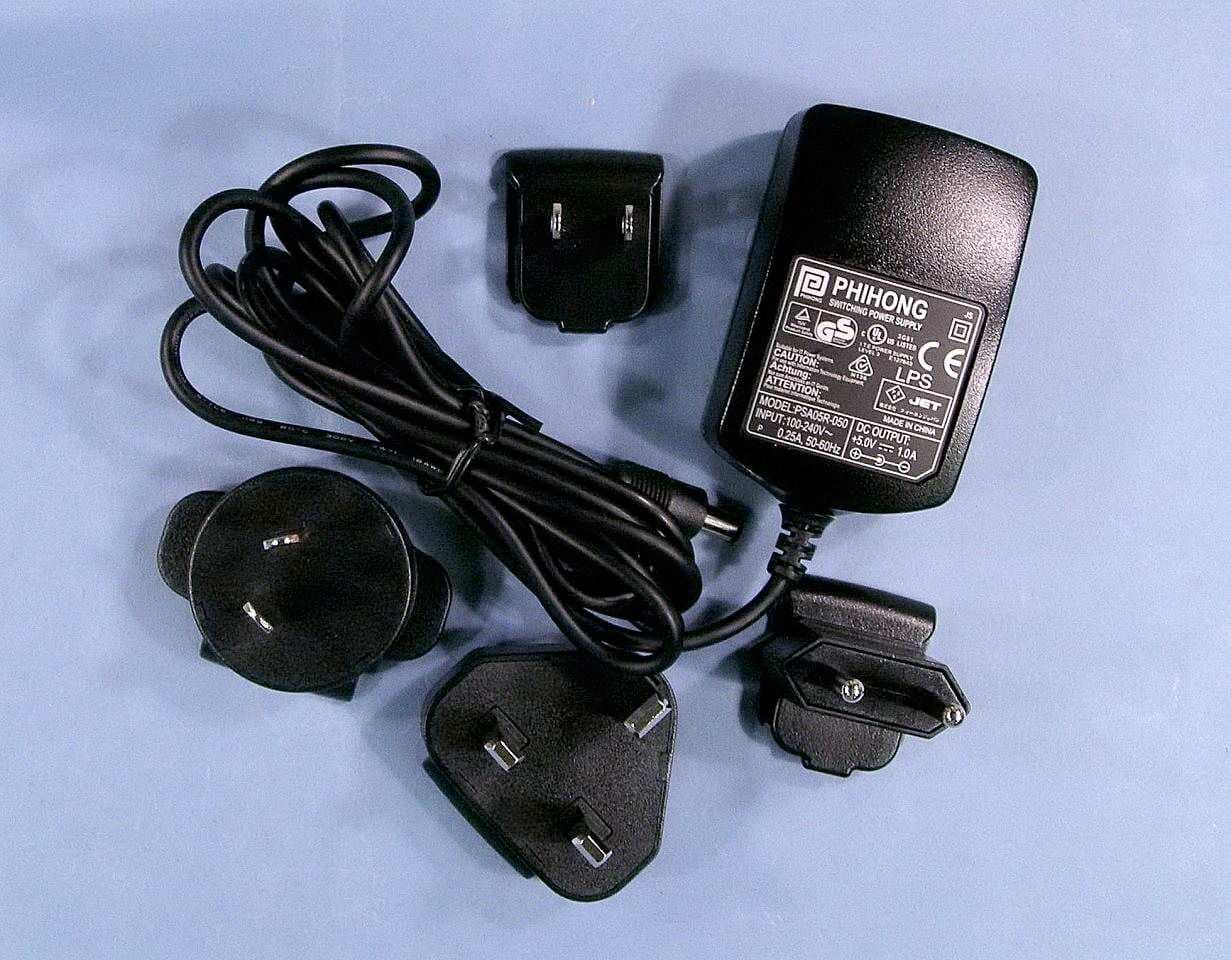
Click to zoom
Application Details
- Equipment Class
- DTS - Digital Transmission System
- Date of Grant
- Mar 07, 2005
- Application Purpose
- Original Equipment
- Date of Application
- Mar 07, 2005
- Equipment Note
- DTS Transceiver
- Frequency Range
- 2405.00000000 - 2480.00000000
- Country
- Denmark
Documents & Files
Document Text
Text extracted from the exhibit documents filed with the FCC. Open a document above to read the original.
Users Manual
MC13192SARDUG/D Rev. 1.4 11/2004 Sensor Applications Reference Design (SARD) User’s Manual How to Reach Us: USA/Europe/Locations Not Listed: Freescale Semiconductor Literature Distribution Center P.O. Box 5405 Denver, Colorado 80217 1-800-521-6274 or 480-768-2130 Japan: Freescale Semiconductor Japan Ltd. Technical Information Center 3-20-1, Minami-Azabu, Minato-ku Tokyo 106-8573, Japan 81-3-3440-3569 Asia/Pacific: Freescale Semiconductor Hong Kong Ltd. 2 Dai King Street Tai Po Industrial Estate Tai Po, N.T., Hong Kong 852-26668334 Home Page: www.freescale.com Information in this document is provided solely to enable system and software implementers to use Freescale Semiconductor products. There are no express or implied copyright licenses granted hereunder to design or fabricate any integrated circuits or integrated circuits based on the information in this document. Freescale Semiconductor reserves the right to make changes without further notice to any products herein. Freescale Semiconductor makes no warranty, representation or guarantee regarding the suitability of its products for any particular purpose, nor does Freescale Semiconductor assume any liability arising out of the application or use of any product or circuit, and specifically disclaims any and all liability, including without limitation consequential or incidental damages. “Typical” parameters that may be provided in Freescale Semiconductor data sheets and/or specifications can and do vary in different applications and actual performance may vary over time. All operating parameters, including “Typicals”, must be validated for each customer application by customer’s technical experts. Freescale Semiconductor does not convey any license under its patent rights nor the rights of others. Freescale Semiconductor products are not designed, intended, or authorized for use as components in systems intended for surgical implant into the body, or other applications intended to support or sustain life, or for any other application in which the failure of the Freescale Semiconductor product could create a situation where personal injury or death may occur. Should Buyer purchase or use Freescale Semiconductor products for any such unintended or unauthorized application, Buyer shall indemnify and hold Freescale Semiconductor and its officers, employees, subsidiaries, affiliates, and distributors harmless against all claims, costs, damages, and expenses, and reasonable attorney fees arising out of, directly or indirectly, any claim of personal injury or death associated with such unintended or unauthorized use, even if such claim alleges that Freescale Semiconductor was negligent regarding the design or manufacture of the part. Learn More: For more information about Freescale products, please visit www.freescale.com. Freescale™ and the Freescale logo are trademarks of Freescale Semiconductor, Inc. All other product or service names are the property of their respective owners. © Freescale Semiconductor, Inc. 2004. All rights reserved. Sensor Application Reference Design, Rev. 1.4 Freescale Semiconductor1 Contents About This Book Audience . . . . . . . . . . . . . . . . . . . . . . . . . . . . . . . . . . . . . . . . . . . . . . . . . . . . . . . . . . . . . . . . . . . . . 3 Organization . . . . . . . . . . . . . . . . . . . . . . . . . . . . . . . . . . . . . . . . . . . . . . . . . . . . . . . . . . . . . . . . . . 3 Conventions . . . . . . . . . . . . . . . . . . . . . . . . . . . . . . . . . . . . . . . . . . . . . . . . . . . . . . . . . . . . . . . . . . 3 Definitions, Acronyms, and Abbreviations . . . . . . . . . . . . . . . . . . . . . . . . . . . . . . . . . . . . . . . . . . 4 References. . . . . . . . . . . . . . . . . . . . . . . . . . . . . . . . . . . . . . . . . . . . . . . . . . . . . . . . . . . . . . . . . . . . 4 Revision History . . . . . . . . . . . . . . . . . . . . . . . . . . . . . . . . . . . . . . . . . . . . . . . . . . . . . . . . . . . . . . . 4 Chapter 1 Introduction and Configuration 1.1Safety Information . . . . . . . . . . . . . . . . . . . . . . . . . . . . . . . . . . . . . . . . . . . . . . . . . . . . . . . . . . . 1-1 1.2MC13192 Sensor Applications Reference Design (SARD) Components . . . . . . . . . . . . . . . . . 1-1 1.3Hardware Description . . . . . . . . . . . . . . . . . . . . . . . . . . . . . . . . . . . . . . . . . . . . . . . . . . . . . . . . . 1-2 1.4Applications and Programming Information . . . . . . . . . . . . . . . . . . . . . . . . . . . . . . . . . . . . . . . 1-8 Appendix A SARD Board Layout and Bill of Materials A.1PCB Layout. . . . . . . . . . . . . . . . . . . . . . . . . . . . . . . . . . . . . . . . . . . . . . . . . . . . . . . . . . . . . . . . . A-1 Sensor Application Reference Design, Rev. 1.4 2Freescale Semiconductor Sensor Applications Reference Design, Rev. 1.4 Freescale Semiconductor3 About This Book This guide provides detailed information about the MC13192 Sensor Applications Reference Design (SARD). The SARD provides all the components to evaluate and use an MC13192. It is intended to allow a system engineer or software developer to gain an understanding of the MC13192 and its protocol. Audience The guide is intended for software and system engineers who are developing their products or software applications making use of the MC13192 to achieve wireless connectivity capability. It is assumed that the reader has a good working knowledge of general-purpose microcontrollers (MCU). Organization The book is divided into 1 chapter and 1 appendix. Chapter 1 introduces the MC13192 Sensor Applications Reference Design (SARD) functionality and features. Appendix A provides figures of the SARD printed circuit board. Conventions This section names, describes, and defines the conventions used in the book. This document uses the following conventions: •OVERBAR is used to indicate a signal that is active when pulled low: for example, RESET . •Logic level one is a voltage that co…
Text truncated - open the document above for the full version.
External Photos
FCC ID: SKA13192-SARD Project no.: 37429-6 Page 4 of 4 Nemko Comlab AS, N-2027 Kjeller AC adapter with different plugs AC adapter with different plugs with numbers FCC ID: SKA13192-SARD Project no.: 37429-6 Page 5 of 5 Nemko Comlab AS, N-2027 Kjeller Supplied accessories for Testing
Internal Photos
FCC ID: SKA13192-SARD Project no.: 37429-6 Page 2 of 2 Nemko Comlab AS, N-2027 Kjeller 13192-SARD, Bottom view 13192-SARD, Top view FCC ID: SKA13192-SARD Project no.: 37429-6 Page 3 of 3 Nemko Comlab AS, N-2027 Kjeller 13192-SARD, view of RS 232 port
Operational Description
Sensor Application Reference Design, Rev. 1.4 1-2Freescale Semiconductor Introduction and Configuration 1.2MC13192 Sensor Applications Reference Design (SARD) Components The MC13192 Sensor Applications Reference Design (SARD) introduces users to the MC13192 2.4 GHz wireless data transceiver. It includes an RS232 port, background debug module for in-circuit hardware debug, switches, LEDs, and a host MCU and allows the user flexibility in establishing wireless data networks. Features of the MC13192 SARD include: •Provides all hardware required for a complete 2.4 GHz wireless node using IEEE 802.15.4 packet structure. •One MC13192 2.4 GHz transceiver RF reference design with printed circuit antenna. •One MC9S08GT60 low-power, low-voltage MCU with 60KB of on-chip Flash. •Background Debug Module (BDM) programming port for support of Metrowerks CodeWarrior™ Development Studio. •Provides IEEE 802.15.4 modem. •Two Accelerometers: MMA6261Q (X and Y axis), MMA1260D (Z axis) •RS-232 port for interface with a personal computer. •Four switches and LEDs for control and monitoring. •Reset switch for program reset. •Scalable software support: — Proprietary point-to-point or star networking using Freescale’s Simple Medium Access Control (SMAC) software — IEEE 802.15.4 Standard compliant networking using Freescale’s MAC/PHY — ZigBee™ networking using Freescale’s Z-stack software 1.3Hardware Description As previously stated, the MC13192 Sensor Applications Reference Design (SARD) provides the hardware required to establish a wireless node using a variety of protocols. Figure 1-1 shows a simplified block diagram of two SARDs connected in a simple point-to-point network. Optional personal computers are shown for control and monitoring. The SARD is a 2 inch x 3 inch module that comprises a complete network node containing the MC13192, crystal, printed circuit antenna and MCU. Also included are jumper-selectable X-Y and Z Axis Accelerometers, four switches, and four LEDs for monitoring purposes. The SARD derives its power from a 9V battery. NOTE Do not use a Lithium battery. Introduction and Configuration Sensor Application Reference Design, Rev. 1.4 Freescale Semiconductor1-3 Figure 1-1. Point to Point MC13192 SARD Block Diagram 1.3.1MC13192 SARD Circuit Description Figure 1-2 shows the MC13192 SARD schematic. Appendix A includes board layout, including the printed dipole receive and transmit antennas, and Bill of Material information. All circuitry required for a 2.4 GHz wireless node is provided. The heart of the design is the MC13192 2.4 GHz transceiver and the MC9S08GT60 microcontroller. All connections for control of the transceiver by the MCU are provided. Peripherally, four LEDs and switches interfacing with the MCU are provided for control and demonstration purposes. Three accelerometers are provided. An MMA6261Q (X and Y axis) and an MMA1260D (Z axis) for demonstration purposes. A Background Debug Module (BDM) port is provided for programming using the CodeWarrior™ Development Studio to develop and in-circuit debug code and program the MCU. An RS-232 interface is provided to allow monitoring or programming. PC RS232 SPI MC13192 SPI MC13192 RS232 PC Node One RF BDM Interface (Programming Only) BDM Interface (Programming Only) X-Y Axis Accelerometer Z Axis Accelerometer Node Two X-Y Axis Accelerometer Z Axis Accelerometer HCS08 MCU HCS08 MCU Sensor Application Reference Design, Rev. 1.4 1-4Freescale Semiconductor Introduction and Configuration Figure 1-2. MC13192 SARD Schematic 55 44 33 22 11 D D C C B B A A MOSI GPIO1 SSIRQCLKOMISOSPICLKRSTBRXTXEN 100_Ohm3 100_Ohm1 GPIO2 ATTNB TxRxCTSRTS 100_Ohm4 100_Ohm5100_Ohm6 100_Ohm2 VDDA V_RS232 3V0 5V0 3V0 3V0 3V0 3V0 3V0 3V0 3V0 3V0 3V0 3V0 V_RS232 5V0 GPIO1GPOI2 GPIO2GPIO1 PTC5PTC6PTG1 PTG1PTA7PTA6 PTA6PTA7 PTC6PTC5 PTC0PTC1 PTC0PTC1 TitleSize Document Number Rev Date: Sheet of C o n f i d e n t i a l I n f o r m a t i o n This document contains Freescale Semiconductor Danmark A/S confidential and proprietary information, whichyou are not entitled to reproduce or disclose to any third party without the prior written consent of FreescaleSemiconductor Danmark A/S.© F r e e s c a l e S e m i c o n d u c t o r D a n m a r k A / S 80000536000_R0202.DSN R02.02 MC13192-SARD (DIG536-2): Main Schematic Skalhuse 5DK-9240 Nibe, DenmarkTelephone: +45 9671 0000 A2 11 Friday, October 29, 2004 JJ 2 0 0 3 - 2 0 0 4 www.freescale.comFax: +45 9835 0052 BDM PORT LED4 LED3 SW3SW4 LED2 LED1 SW1SW2 Z Axis ACCX-Y Axis ACC 9V battery + - + -2-3V battery SW5 RESET Switch A102Secundary fiducial point (Compside) C1144.7μF C112100nF HOLE103np hole ø2.2mm C1164.7μF C120100nF R1091.0K BARCODE101Label 26*13mm Test BarCode W103EL=8.0 deg, Z=115ohm IC104MMA6261Q XOUT 15 N/C 11 N/C 10 N/C 9 N/C 8 N/C 6 N/C 5 N/C 1 N/C 2 N/C 7 N/C 16 VSS 4 VDD 3 EP 17 ST 12 N/C 13 YOUT 14 C107220pF D104Green LED C12618pF C1231μFNot Mounted ANT102 X101 16.000MHz R104220R R1121.0K A103Secundary fiducial point (Soldside) C101100nF C102100nF S101 Switch SPST SMD C1154.7μF C111100nF J1032p 1 2 R106220RNot Mounted IC106MMA1260D N/C 15 N/C 11 N/C 10 N/C 9 ST 8 VDD 6 STATUS 5 VSS 1 VSS 2 VSS 7 N/C 16 VOUT 4 VSS 3 N/C 12 N/C 13 N/C 14 J1012*3p 1 2 3 4 5 6 W104EL=8.0 deg, Z=115ohm C103100nF C124100nF R1131.5K A101Primus datum point (Compside) S103 Switch SPST SMD C1056.8pF C1281.5pF C1171μF D101Green LED R103220R J102 9p Female Ang 594837261 m1m2 J108 9V Holder and Connector - Female 1 2 3 C109100nF IC102MC9S08GT60 IRQ 11 PTA0/KBIP0 32 PTA1/KBIP1 33 PTA2/KBIP2 34 PTA3/KBIP3 35 PTA4/KBIP4 36 PTA5/KBIP5 37 PTA6/KBIP6 38 PTA7/KBIP7 39 PTB0/AD0 22 PTB1/AD1 23 PTB2/AD2 24 PTB3/AD3 25 PTB4/AD4 26 PTB5/AD5 27 PTB6/AD6 28 PTB7/AD7 29 PTC0/TxD2 2 PTC1/RxD2 3 PTC2/SDA 4 PTC3/SCL 5 PTC4 6 PTC5 7 PTC6 8 PTD0/TPM1CH0 18 PTD1/TPM1CH1 19 PTD3/TPM2CH0 20 PTD4/TPM2CH1 21 PTE0/TxD1 9 PTE1/RxD1 10 PTE2/SS 12 PTE3/MISO 13 PTE4/MOSI 14 PTE5/SPSCK 15 PTG0/BKGD/MS 42 PTG1/XTAL 43 PTG2/EXTAL 44 RESET 1 VDD 17 VDDAD 40 VREFH 30 VREFL 31 VSS 16 …
Text truncated - open the document above for the full version.
Test Report
Total no. of Pages : 34 Test report : 37429-6 Item tested : 13192-SARD Type of equipment : Zigbee transceiver FCC ID : SKA13192-SARD Client : Freescale Semiconductor Danmark A/S Tested according to : FCC part 15.247 DTS Transmitter 2405 - 2480 MHz Date of issue : 05 MARCH 2005 Authorized by : The results detailed in this test report applies only to the particular sample(s) tested and with configuration(s) as implemented during testing. This test report shall not be reproduced, except in full, without the written approval of Nemko Comlab AS. Any use which a third party makes of this report, or any reliance on or decisions to be made based on it, are the responsibility of such third parties. Nemko Comlab AS accepts no responsibility for damages, if any, suffered by any third party as a result of decisions made or actions based on this report. Test Report FCC ID: SKA13192-SARD Project no.: 37429-6 Page 2 of 34 Nemko Comlab AS, N-2027 Kjeller CONTENTS 1 GENERAL INFORMATION ...........................................................................................................3 1.1 Test house Info ............................................................................................................3 1.2 Client Information .........................................................................................................3 1.3 Manufacturer ................................................................................................................3 2 Test Information ............................................................................................................................4 2.1 Tested Item ..................................................................................................................4 2.2 Test Environment .........................................................................................................4 2.3 Test Period...................................................................................................................4 3 TEST REPORT SUMMARY..........................................................................................................5 3.1 General ........................................................................................................................5 3.2 Test Summary..............................................................................................................6 3.3 Description of modification for Modification Filing .......................................................6 3.4 Comments....................................................................................................................6 3.5 Family List Rational......................................................................................................6 4 TEST RESULTS............................................................................................................................7 4.1 Power line Conducted Emissions ................................................................................7 4.2 Bandwidth ..................................................................................................................10 4.3 Peak Power Output....................................................................................................13 4.4 Out-of-band emissions (Radiated).............................................................................16 4.5 Power Spectral Density (PSD)...................................................................................27 4.6 Upper Band Edge Radiated Emissions .....................................................................30 LIST OF TEST EQUIPMENT .........................................................................................................32 5 BLOCK DIAGRAM ......................................................................................................................33 5.1 System set up ............................................................................................................33 5.2 Power line Conducted Emission ................................................................................33 5.3 Test Site Radiated Emission and peak power output................................................34 Test Report FCC ID: SKA13192-SARD Project no.: 37429-6 Page 3 of 34 Nemko Comlab AS, N-2027 Kjeller 1 GENERAL INFORMATION 1.1 Test house Info Name : Nemko Comlab AS Address : Gåsevikveien 8, Box 96 N-2027 Kjeller, NORWAY Telephone : +47 64 84 57 00 Fax : +47 64 84 57 05 E-mail: mailto:[email protected] Managing Director: Kjell G. Haga FCC test firm registration number : 994405 Industry Canada OATS registration number : 4443 1.2 Client Information Name : Freescale Semiconductor Danmark A/S Address : Skalhuse 5, 9240 Nibe, Denmark Telephone : +45 967 10 000 Fax : +45 983 50 052 Contact: Name : Johnny Jonassen Telephone : +45 967 12 153 E-mail : [email protected] 1.3 Manufacturer Name : Freescale Semiconductor Danmark A/S Address : Skalhuse 5, 9240 Nibe, Denmark Telephone : +45 967 10 000 Fax : +45 983 50 052 Test Report FCC ID: SKA13192-SARD Project no.: 37429-6 Page 4 of 34 Nemko Comlab AS, N-2027 Kjeller 2 Test Information 2.1 Tested Item Name : 13192-SARD FCC ID : SKA13192-SARD Model/version : 13192-SARD Serial number : Marked on PCB “13192-SARD” Hardware identity and/or version: 80000536000_R0300 Software identity and/or version : PTC Version 1.05 Frequency Range : 2405 - 2480 MHz Tunable Bands : 1 Number of Channels : 16 1 Modulation : 0-QPSK Emissions Designator : G1D User Frequency Adjustment : None, Software controlled. Rated peak Output Power : 10 mW 1) 16 channels in use. Theory of Operation The 13192-SARD is a “Zigbee” low data rate wireless device according to IEEE 802.15.4, with 5MHz channel bandwidth. 2.2 Test Environment 2.2.1 Normal test condition Temperature: 20 - 23 °C Relative humidity: 29 - 50 % Normal test voltage: 9.0 V DC The values are the limit registered during the test period. 2.3 Test P…
Text truncated - open the document above for the full version.
Test Setup Photos
FCC ID: SKA13192-SARD Project no.: 37429-6 Page 1 of 1 Nemko Comlab AS, N-2027 Kjeller PHOTOS OF TEST SET-UP AND THE TESTED EQUIPMENT Radiated emission above 1 GHz Test setup, Conducted emissions
Contact Information
Applicant
Johnny Jonassen(R&D Engineer)
Technical Contact
Test Firm
Nemko ASFrode Sveinsen
Technical Specifications
| # | Rule Parts | Frequency Range | Power Output |
|---|---|---|---|
| 1 | 15C | 2.40 GHz - 2.48 GHz | 22.00 mW |
Other Applications from Freescale Semiconductor Danmark A/S
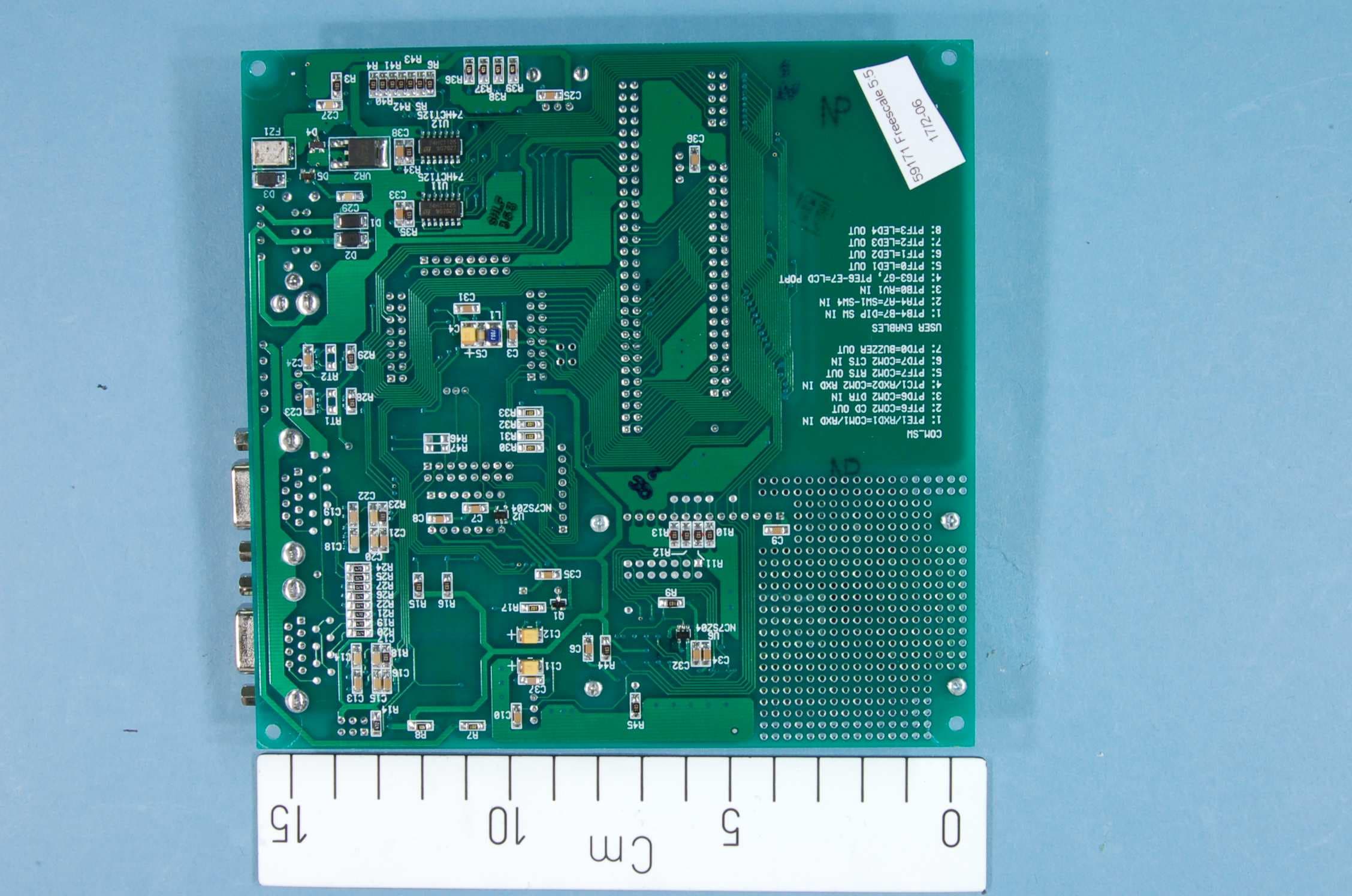
SKA13202-RFD
Mar 15, 2006IEEE 802.15.4 Transceiver
Equipment Class
DTS - Digital Transmission System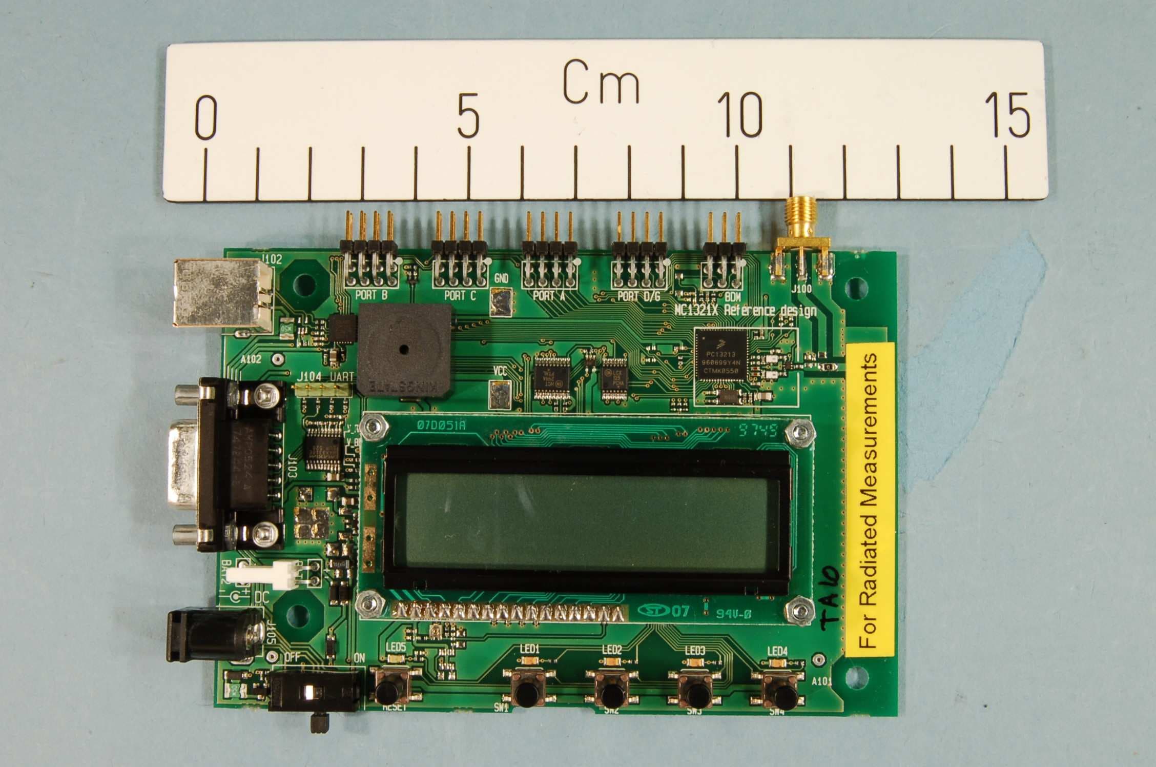
SKA13213-NCB
Mar 08, 2006IEEE 802.15.4 Transceiver
Equipment Class
DTS - Digital Transmission System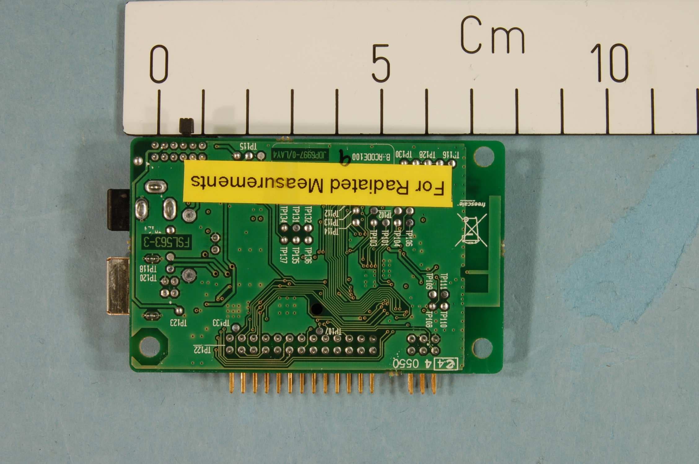
SKA13213-SRB
Mar 08, 2006IEEE 802.15.4
Equipment Class
DTS - Digital Transmission System